True Random Number Generator Implemented in ReRAM Crossbar Based on Static Stochasticity of ReRAMs

Adv. Sci. Technol. Eng. Syst. J. 9(5), 30–36 (2024);
 DOI: 10.25046/aj090504
True Random Number Generators (TRNG) find applications in various fields, especially hardware security. We suggest a TRNG that exploits the intrinsic static stochasticity of Resistive Switching Random Access Memories (ReRAMs) to generate random bits. Other suggested designs use stochasticity in the switching mechanism, which requires high precision over input voltage and time. In the proposed design, the random bits are produced by comparing the resistance of two ReRAMs in their high resistance states. ReRAM crossbar architectures are being highly researched, and our design is completely compatible with a ReRAM crossbar. The design was verified by simulations and testing the output stream using the NIST randomness test suite. The effect of device-to-device variability was tested on the randomness of the generated output bit stream.
1. Introduction
This paper is an extension of work originally presented in The IEEE Asia Pacific Conference On Circuits And Systems (APCCAS 2023) [1]. Random Numbers find a lot of applications in various fields, including scientific simulations and modeling, games, machine learning, and, most importantly, generating cryptographic keys [2, 3, 4]. Random numbers are generated using specialized hardware called Random Number Generators (RNGs). There are two types of RNGs, Pseudo Random Number Generators (PRNGs) and True Random Number Generators (TRNGs), differentiated based on the principle of number generation. PRNGs generate random numbers using algorithms based on mathematical formulae. While PRNGs are suitable for other applications, they cannot be used for security applications as they are vulnerable to attacks [5, 6], compromising security. TRNGs exploit the stochasticity of physical processes, e.g., Thermal Noise in electrical circuits [7], to generate random numbers. Since the source of randomness in TRNGs is inherently stochastic, they, in principle, can guarantee absolute information security.
Recently, there has been an increase in IoT devices in the market, which are small and have a small power budget. Since they continuously transmit confidential and private information, there is a need for a robust security system within the devices, necessitating a suitable TRNG to generate random numbers for encryption [8, 9]. Current TRNG circuits are made of transistors and are based on thermal noise, jitter in oscillators, random telegraph noise, or chaotic systems [10, 11, 12]. These circuits are bulky, complicated, and consume a lot of power, making them unsuitable for IoT devices.
ReRAM devices can be used as an alternative to design TRNGs. ReRAMs are emerging non-volatile memory devices extensively researched for crossbar architecture. This crossbar architecture finds applications in non-volatile logic, neuromorphic computing, security, in-memory computing, etc. [13, 14]. They consume low power, are small, are compatible with the CMOS fabrication process, and have fast switching speeds. They are also inherently stochastic, making them a good alternative for TRNG circuit design. ReRAMs exhibit stochasticity in two ways – during switching and the resistance values of the stable states. Many ReRAM-based TRNG designs have been suggested in the literature before, mainly focusing on switching stochasticity [15, 16, 17]. These designs require very precise control over voltages and timing, making the circuits complicated to implement. The variability in the resistance value can also be exploited to design TRNG circuits. Since they do not require precise control of input signals, they are easier to implement. One such design compares the resistance value of two devices to extract the output bit [18].
We propose a TRNG circuit based on the above principle, implementable in a ReRAM crossbar. This enables in-situ random number generation for crossbar applications and eliminates the need for a specialized TRNG circuit. The proposed circuit is simulated in Cadence Virtuoso™, and the randomness of the output is verified using the NIST SP 800-22 test suite [19]. We further analyzed the effect of variation in the statistical properties of ReRAM stochasticity on the randomness of the output. This paper is organized as follows. The theory of ReRAM and its stochasticity is explained in section 2. The simulation setup is described in section 3. The design and results are discussed in section 4. Analysis of variation in device properties on output is done in section 5. Conclusion from this work are presented in section 6.
2. Theory
2.1. Resistive Switching Random Access Memory (ReRAM)
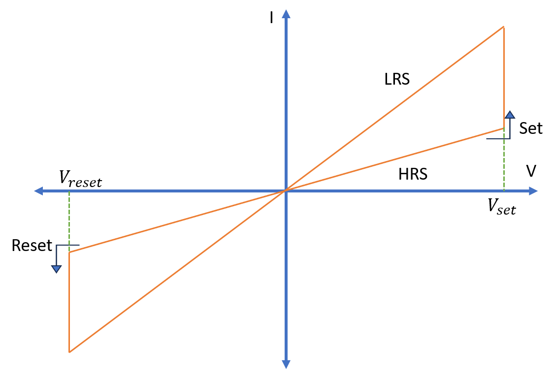
ReRAM is a two-terminal, non-volatile emerging memory device belonging to the family of memristive devices [20, 21]. A memristor, derived from “Memory” and “Resistor,” is a two-terminal device whose resistance equals the total amount of charge flown through it. Consequently, the resistance of a ReRAM can be controlled by applying a voltage across the electrodes, and the device can retain its state until an appropriate voltage is applied to change the state. ReRAM consists of a Metal-Insulator-Metal (MIM) stack where the insulator is generally metal oxide. The device works on the principle of ion migration, where ions migrate through the insulator from one terminal to the other, forming a conductive filament when voltage is applied. ReRAM has two states – Low Resistance State (LRS) and High Resistance State (HRS). The conductive filament, formed by the migration of ions, provides a path for current to flow between the filaments, setting the device in the LRS. Switching from HRS to LRS is known as setting the device, and the voltage at which it occurs is known as set voltage. The device is reset when it switches from LRS to HRS; the applied voltage is known as reset voltage. When the magnitude of the applied voltage is greater than the magnitude of the reset voltage, the conductive filament is ruptured. When the magnitude of the applied voltage is less than the set or reset voltage, the device retains its state. The I-V graph of a typical ReRAM device is shown in Figure 1. The state of the device can be sensed by applying a read voltage less than the set/reset voltage and measuring the current.
2.2. Stochasticity in ReRAM
ReRAMs suffer broadly from two types of stochasticity – Dynamic and Static. Dynamic stochasticity is observed during the switching of the states, and variability can be observed in switching voltages and the time required for the device to switch from one state to an- other [22]. The probability of switching is also random and follows a lognormal distribution [23]. The switching probability increases with an increase in programming amplitude and time for which the voltage pulse is applied. Static stochasticity is the variability in the final resistance value of the device in LRS and HRS. This variability closely follows a lognormal probability density function [24, 25, 26] and hence is modeled as such. The cycle-to-cycle variation in resistance values and switching probabilities is because the filament formation and rupture cannot be precisely controlled in every cycle. The filament’s width and length vary from one cycle to another. This is more significant in HRS as the filament length, after breaking, can take up any value as long as it is disconnected from the terminal. This is observed in the device’s resistance values, as the resistance variation is much more significant in HRS than in LRS [18]. The inherent dynamic and static stochasticity can be exploited to extract random numbers. The time or voltage required to switch is used in many proposed circuits, but as mentioned earlier, precise control of applied voltage and pulse timing is required, which makes the design complicated. Extracting random bits using static stochasticity is easier because the device is in a stable state, and as long as these states are reached, there is no need for precise control of the input signals. We exploit the significant variance in HRS resistance stochasticity in our proposed design.
3. Simulation
The working of the proposed design was verified by simulation, and further analysis of the variation of device parameters on the randomness of the output was also done. To simulate the ReRAM device, we used the Stanford-PKU RRAM Model [27]. The device is written in Verilog-A and modeled using an internal variable that corresponds to the length of the conductive filament in a device. While a device may have multiple filaments between the two termi- nals, the model uses a single filament, which acts as a cumulation of all the filaments. The increase in the internal variable corresponds to the growth of filament, and the decrease corresponds to decay. The change in the variable is dependent on the voltage across the terminal. To ensure that the device switches states, the set and reset voltages are set to 2 and -2 volts, respectively, greater than the set and reset voltage of the device, and the read voltage is set to 0.5 volts. The switching behavior of the model is shown in Figure 2.
The resistance of the device is dependent on the gap (g) between the end of the conductive filament and the terminal opposite to the temperature and is given by (1).
![]()
L is the device length, and l, the internal variable, is the length of the filament. If the read voltage is kept constant for the model, the device’s resistance is exponentially proportional to g. In other words, the device’s resistance in HRS increases exponentially with an increase in g, as shown in Figure 3. A random value of g is picked from a normal distribution given by (2) to simulate the cycle- to-cycle variation in the device’s resistance.
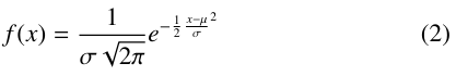
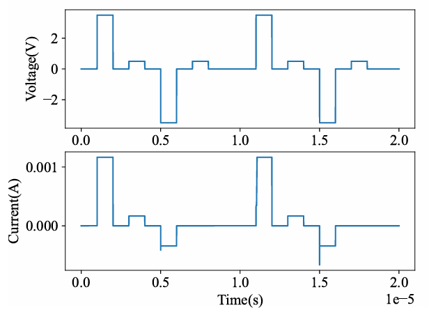
Figure 2: Switching of the states in Stanford-PKU RRAM Model.
µ is the mean of the distribution, and σ is the standard deviation. The variation of the random values can be changed by tweaking the values of µ and σ. For the initial simulations, µ was set to 3 nm, and σ was set to 0.1 nm. Since the device’s resistance is exponentially related to g, it follows a log-normal distribution when g follows a normal distribution. The cycle-to-cycle variation of HRS for 10000 cycles is shown in Figure 4 and matches the trend followed by the device in [18]. To verify the proposed design, we have picked the same µ and σ for all the devices. The effect of different µ and σ on the output is studied in section 5.
The design requires other circuit components like switches, diodes, and a current direction sensor. We wrote Verilog-A codes for the ideal behavior of these circuits for simulation. The ideal components help us verify the working of our proposed design with- out affecting the working principle. The switches were modeled after transmission gates controlled by an external voltage source. The diodes have a forward bias voltage drop of 0.7 V. The current direction sensor is programmed to output 1 when the current is positive and 0 when the current is positive.

4. Design and Results
4.1. Working Principle
The working principle for the proposed design is based on the pro- posed circuit in [18]. In every cycle, two devices are set and then reset to HRS. The devices independently acquire a random resistance value from a log-normal distribution. The resistance values of these two devices are then compared, and the output bit is decided depending on which of the devices has greater resistance. The resistance value in HRS is used because the resistance variation is more significant than LRS.
4.2. Single Bit Design
Our primary aim was to propose a design compatible with a ReRAM crossbar. The proposed design, shown in Figure 5, utilizes a single column of the crossbar and generates one bit per cycle. The design uses two ReRAMs (M1, M2) as the source of randomness and one ReRAM (M3) for bit extraction (explained later). The design uses transmission gates (T1-T5), controlled by voltage sources (C1-C5), as switches. The transmission gates connect the devices to different voltage sources and ground. The design also uses current sensors that sense the current flow direction. The TRNG operation consists of the following steps:
- One terminal of all three ReRAMs, M1, M2, and M3, is connected to the ground, and the devices are set into LRS by applying a set voltage of 2 V to the other terminal of the
- All three devices are disconnected from the ground. One of the terminals of M1 and M2 is connected to one of the terminals of The other terminals of M1 and M2 are connected to their respective voltage sources, and the other terminal of M3 is connected to the current sensor.
- Read voltage of magnitude 500 mV, and opposite amplitude is applied to M1 and M2 through the voltage sources.
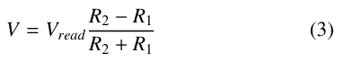
- The voltage at the common terminal of M1 and M2 is given by the (3), where R1 and R2 is the resistance of M1 and M2
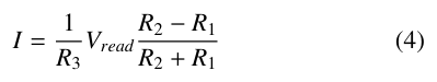
The voltage is positive and negative depending on the resistance values of M1 and M2, and so is the current direction through the current sensor, given by (4), where R3 is the resistance of M3.
The current is positive (negative) if the resistance of M1 is smaller (greater) than the resistance of M2.
5. The output bit is decided by the direction of the current sensed by the current The output bit is 1 if the current is positive and 0 if it is negative.
6. All the ReRAMs are again set to LRS for the next cycle.

The working of the circuit can be seen in Figure 6. The gap, g, and hence the resistance of M1, is lower in cycle one and greater in cycle two than M2. The current through the current sensor is positive and negative in cycles 1 and 2, respectively, as predicted.
4.3. Multi-bit Design
The same principle can be extended to multiple columns in parallel to extract multiple bits in the same cycle. The bits can be read primarily in two ways. Read voltage can be applied multiple times while reading from different columns each time. Or, the bits can be read simultaneously. The second option will consume less time but require more hardware for parallel operation. For verification purposes, we read the output from each column one after the other by applying multiple read signals. The multi-bit design is implemented using a 2×3 ReRAM crossbar and one row of read ReRAMs, considered part of the peripheral circuit, as shown in Figure 7. The design produces three bits per cycle.
The main challenge with using multiple columns is the sneak path current from one column to another, affecting the output bits. We added diodes in the read row to prevent the sneak path current. The diodes prevent the flow in the reverse direction because it is in reverse bias, and since the forward bias voltage is less than the threshold voltage of the diode, no current flows in the forward direction as well. The set voltage applied to the read row is increased to ensure that all ReRAMS are set. The number of bits generated per cycle can be easily increased by increasing the number of columns. However, the number of columns will be limited by the maximum voltage that can be applied as the set voltage for the read row. Also, multiple applications of read voltages in a single cycle may affect the result of the later columns as the devices in these columns may change their state.
4.4. Results and Discussion
Determining the randomness of a sequence of numbers is a challenging task. Generally, a sequence must pass a set of statistical tests to be considered random. We use the NIST SP 800-22 [19] suite of statistical tests to test the sequence generated during the single-bit and multi-bit design simulations. The suite consists of various tests, and a p-value is calculated for each test. If the p-value exceeds 0.01, the sequence passes that particular test. 10,000 bits were generated; their test results are shown in table 1 for single-bit and multi-bit. The generated bit stream passed all the major tests.
The results show that our design can produce a sequence of random numbers. One point to note is the use of ideal switches, diodes, and current sensors for the simulation. We assume that replacing the ideal devices with practical ones will not affect the function of the circuit as long as we ensure that the ReRAMs switch their states, as the design only concerns the final state of the device. The practical devices will mainly affect the set and reset voltages to be applied. This also makes the design immune to variability in threshold voltage and switching time. This flexibility allows the circuit to work with any device as long as the device shows variation in one of the stable states.
The major benefit of the design is that it eliminates the need for additional circuitry to generate random bits. Whenever random bits are required, they can be generated in situ by dedicating some columns of a crossbar for generation. While designing a multi-bit circuit, the designer has the freedom to choose between the number of bits generated per cycle and time per cycle, depending on the constraints.
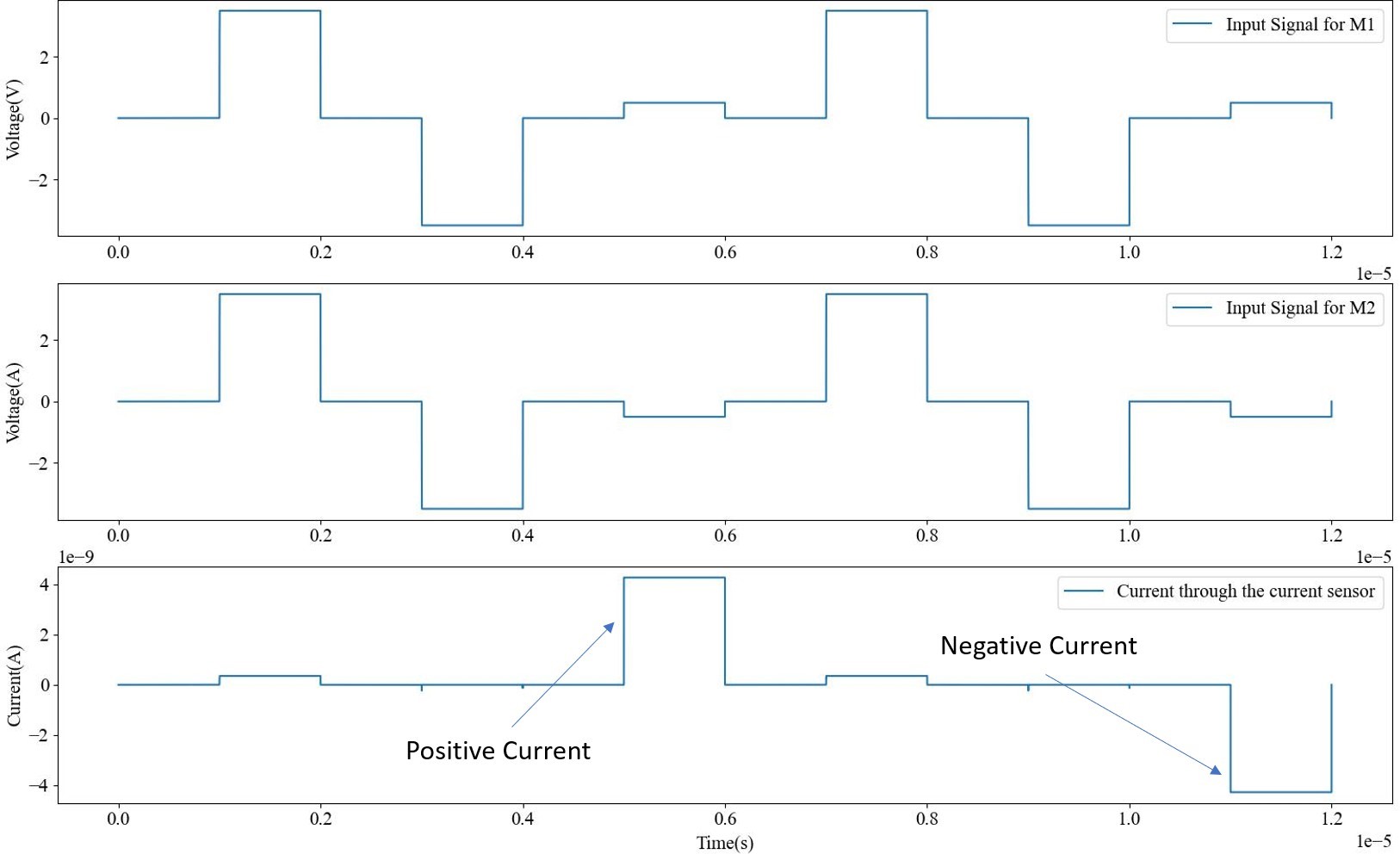

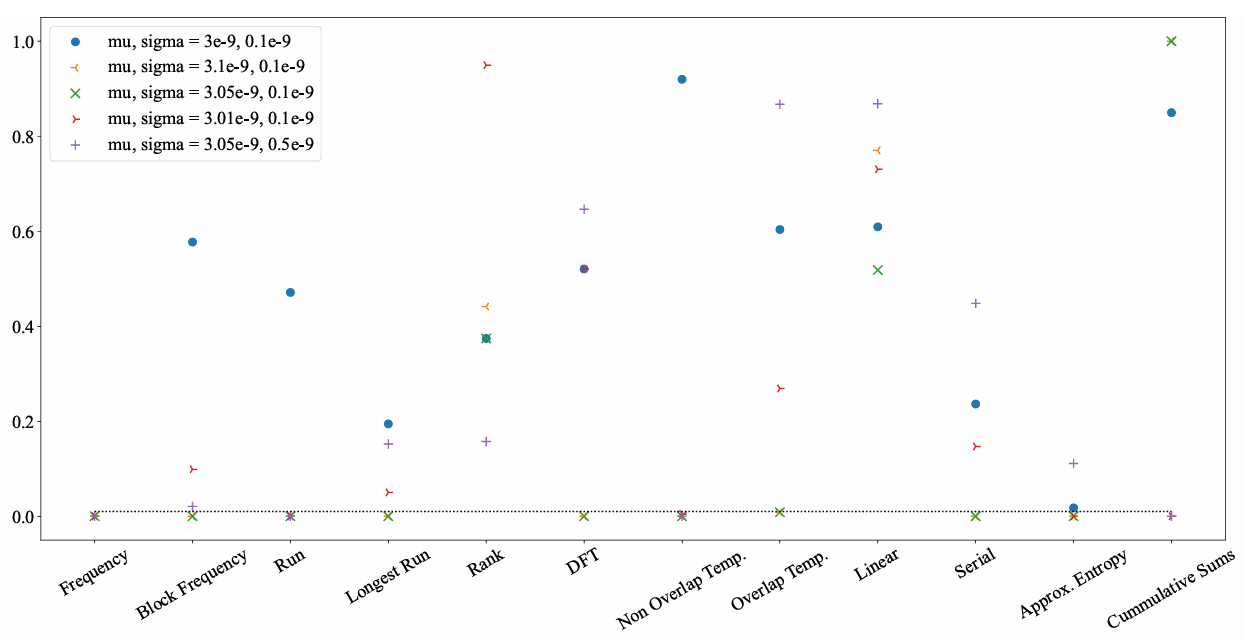
Table 1: NIST Test Result for Single and Multi Bit Circuit
| Test | Single Bit | Multi Bit | ||
| p-value | Result | p-value | Result | |
| Frequency | 0.825 | Random | 0.355 | Random |
| Block Freq. | 0.577 | Random | 0.356 | Random |
| Run | 0.471 | Random | 0.591 | Random |
| Long Run | 0.194 | Random | 0.932 | Random |
| Rank | 0.374 | Random | 0.368 | Random |
| DFT | 0.520 | Random | 0.710 | Random |
| Non-Overlap Temp. | 0.919 | Random | 0.221 | Random |
| Overlap Temp. | 0.603 | Random | 0.932 | Random |
| Linear | 0.609 | Random | 0.147 | Random |
| Serial | 0.236 | Random | 0.368 | Random |
| Approx. Entropy | 0.0177 | Random | 0.586 | Random |
| Cumm. Sum | 0.849 | Random | 0.651 | Random |
5. Analysis of Statistical Variation
The output’s randomness depends on the device properties’ stochastic variation. The proposed design involves two devices simultaneously to extract the random bit. The statistical parameters for the random distribution, µ and sigma, were matched for the two devices to verify the working of the circuit. It is also essential to see the effect on the output’s randomness if these values are mismatched for the two devices. This analysis is critical to understanding the limitations of the circuit design because of device-to-device variation during fabrication. Bits were extracted by changing the µ and σ of one of the devices, and the randomness of the bit stream was tested using the NIST test suit. The results of different tests are shown in Figure 8.
First, the effect of different mean distances (g) for the two de- vices was checked by increasing the µ for one device by 3.33%. As seen from the graph, the extracted bits fail to pass most of the tests. Even after decreasing the increase in µ to 1.67%, the bit stream does not pass most tests. Finally, when µ is increased by just 0.33%, the device’s output passes most of the test. It can be concluded that the output is very sensitive to device mismatches. The circuit can only tolerate a very low difference in the mean of the gap before it starts generating a non-random output. Thus, very close attention must be paid to device mismatch while fabricating the circuit. An interesting observation is made when the σ of the distribution is also changed when changing µ. Increasing the σ by 400% when the µ of one of the devices is increased by 1.67%, results in the output passing more tests. Hence, a more significant cycle-to-cycle variation can tackle a greater device-to-device variation. While a greater variation is detrimental to most circuits, it benefits the proposed circuit.
6. Conclusion
The proposed TRNG uses inherent randomness in the resistance value of HRS to generate random bits. The design is entirely implementable in ReRAM crossbars. The resistance value of two ReRAMs in HRS in a crossbar is compared, and the output bit depends on their relative values. Circuits for generating both one and multi-bit per cycle are suggested. The circuits were simulated, and the generated bit stream passed almost all NIST randomness test suite tests. The design allows for choosing operating parameters without changing the hardware and will be compatible with various types of ReRAM. Significant device-to-device variability results in the output bit stream being not random. The effect can be negated by a more significant cycle-to-cycle variation, which is unsuitable for other applications but positively impacts the random number generation application.
Future work will focus on implementing the design on actual hardware and validating the functioning of the design. It will be crucial to study whether the output is affected when the ideal de- vices are replaced with actual devices and, if so, how. The effect of adjacent columns on the output is also a potential scope of study.
- T. Patni, A. Pethe, “True Random Number Generator Implemented in ReRAM Crossbar Based on Static Stochasticity of ReRAMs,” 2023 IEEE Asia Pacific Conference on Circuits and Systems (APCCAS), 7:55–59, 2023, DOI: 10.1109/APCCAS60141.2023.00024
- P. L’Ecuyer, “Random numbers for simulation,” Commun. ACM, 33, 10:85–97, 1990, DOI: 10.1145/84537.84555
- A. J. Menezes, S. A. Vanstone, P. C. Van Oorschot, Handbook of Applied Cryptography (1st. ed.), CRC Press, Inc., USA, 1996
- D. Eastlake, J. Schiller, S. Crocker, “RFC4086: Randomness Requirements for Security,” RFC, 2005, https://tools.ietf.org/html/rfc4086
- Z. Gutterman, B. Pinkas, T. Reinman, “Open to Attack: Vulnerabilities of the Linux Random Number Generator,” Black Hat, 2006, https://www.blackhat.com/presentations/bh-usa-06/BH-US-06- Gutterman.pdf
- J. Kelsey, B. Schneier, D. Wagner, C. Hall, “Cryptanalytic Attacks on Pseudorandom Number Generators,” Fast Software Encryption, FSE 1998, Lecture Notes in Computer Science, 1372:12, Springer, Berlin, Heidelberg, 1998, DOI: 10.1007/3-540-69710-1 12
- L. Gong, J. Zhang, H. Liu, L. Sang, Y. Wang, “True Random Number Generators Using Electrical Noise,” IEEE Access, 7:125796–125805, 2019, DOI: 10.1109/ACCESS.2019.2939027
- A. Vassilev, T. Hall, “The Importance of Entropy to Information Security” Computer, 47, 02:78–81, 2014, DOI: 10.1109/MC.2014.47
- Z. Liu, D. Peng, “True random number generator in RFID systems against traceability,” CCNC 2006. 2006 3rd IEEE Consumer Communications and Networking Conference, 620–624, 2006, DOI: 10.1109/CCNC.2006.1593098
- F. Pareschi, G. Setti, R. Rovatti, “Implementation and Testing of High-Speed CMOS True Random Number Generators Based on Chaotic Systems,” IEEE Transactions on Circuits and Systems I: Regular Papers, 57, 12:3124–3137, 2010, DOI: 10.1109/TCSI.2010.2052515
- M. Park, J. C. Rodgers, D. P. Lathrop, “True random number generation using CMOS Boolean chaotic oscillator,” Microelectronics Journal, 46, 12, Part A:1364–1370, 2015, DOI: 10.1016/j.mejo.2015.09.015
- N. Nguyen, G. Kaddoum, F. Pareschi, R. Rovatti, G. Setti, “A fully CMOS true random number generator based on hidden attractor hyperchaotic system,” Nonlinear Dyn, 102:2887–2904, 2020, DOI: 10.1007/s11071-020-06017-3
- F. Zahoor, T. Z. Azni Zulkifli, F. A. Khanday, “Resistive Random Access Memory (RRAM): an Overview of Materials, Switching Mechanism, Performance, Multilevel Cell (mlc) Storage, Modeling, and Applications,” Nanoscale Res Lett, 15:90, 2020, DOI: 10.1186/s11671-020-03299-9
- F. Zahoor, F. A. Hussin, U. B. Isyaku, S. Gupta, F. A. Khanday, A. Chattopadhyay, H. Abbas, “Resistive random access memory: introduction to device mechanism, materials and application to neuromorphic computing,” Discover Nano, 18:36, 2023, DOI: 10.1186/s11671-023-03775-y
- H. Jiang, D. Belkin, S. E. Savel’ev, S. Lin, Z. Wang, Y. Li, S. Joshi, R. Midya, C. Li, M. Rao, M. Barnell, Q. Wu, J. J. Yang, Q. Xia, “A novel true random number generator based on a stochastic diffusive memristor,” Nat Commun, 8:882, 2017, DOI: 10.1038/s41467-017-00869-x
- B. Yang, D. Arum´ı, S. Manich, A´ . Go´mez-Pau, R. Rodr´ıguez-Montan˜e´s, M. B. Gonz´alez, F. Campabadal, L. Fang, “RRAM Random Number Generator Based on Train of Pulses,” Electronics, 10:1831, 2021, DOI: 10.3390/electronics10151831
- J. Postel-Pellerin, H. Bazzi, H. Aziza, P. Canet, M. Moreau, V. D. Marca, A. Harb, “True random number generation exploiting SET voltage variability in resistive RAM memory arrays,” 2019 19th Non-Volatile Memory Technology Symposium (NVMTS), 1-5, 2019, doi: 10.1109/NVMTS47818.2019.9043369
- T. Zhang, M. Yin, C. Xu, X. Lu, X. Sun, Y. Yang, R. Huang, “High-speed true random number generation based on paired memristors for security electronics,” Nanotechnology, 28:455202, 2017, doi: 10.1088/1361-6528/aa8b3a
- L. E. Bassham, A. L. Rukhin, J. Soto, J. R. Nechvatal, M. E. Smid, E. B. Barker, S. D. Leigh, M. Levenson, M. Vangel, D. L. Banks, N. A. Heckert, J. F. Dray, S. Vo, “SP 800-22 Rev. 1a. A Statistical Test Suite for Random and Pseudorandom Number Generators for Cryptographic Applications,” Technical Report, National Institute of Standards & Technology, Gaithersburg, MD, USA, 2010
- L. O. Chua, S. M. Kang, “Memristive devices and systems,” Proceedings of the IEEE, 64, 2:209-223, 1976, doi: 10.1109/PROC.1976.10092
- T. Prodromakis, C. Toumazou, “A review on memristive devices and applications,” 2010 17th IEEE International Conference
on Electronics, Circuits and Systems, 934-937, 2010, doi: 10.1109/ICECS.2010.572466610.1109/ICECS.2010.5724666 - R. Degraeve, A. Fantini, N. Raghavan, L. Goux, S. Clima, B. Govoreanu, A. Belmonte, D. Linten, M. Jurczak, “Causes and consequences of the stochastic aspect of filamentary RRAM,” Microelectronic Engineering, 147:171-175, 2015, 10.1016/j.mee.2015.04.025
- G. Medeiros-Ribeiro, F. Perner, R. Carter, H. Abdalla, M. D. Pickett, R. S. Williams, “Lognormal switching times for titanium dioxide bipolar memristors: origin and resolution,” Nanotechnology, 22, 9:095702, 2011, 10.1088/0957- 4484/22/9/095702
- Y. Wang, W. Wen, H. Li, M. Hu, “A Novel True Random Number Generator Design Leveraging Emerging Memristor Technology,” Proceedings of the 25th edition on Great Lakes Symposium on VLSI (GLSVLSI ’15), 271-276, 2015, 10.1145/2742060.2742088
- M. Hu, Y. Wang, Q. Qiu, Y. Chen, H. Li, “The stochastic modeling of TiO2 memristor and its usage in neuromorphic system design,” 2014 19th Asia and South Pacific Design Automation Conference (ASP-DAC), 831-836, 2014, 10.1109/ASPDAC.2014.6742993
- S. Yu, B. Gao, Z. Fang, H. Yu, J. Kang, H. S. P. Wong, “Stochastic learning in oxide binary synaptic device for neuromorphic computing,” Frontiers in Neuroscience, 7, 2013, 10.3389/fnins.2013.00186
- H. Li, Z. Jiang, P. Huang, Y. Wu, H.-Y. Chen, B. Gao, X. Y. Liu, J. F. Kang, H.- S. P. Wong, “Variation-aware, reliability-emphasized design and optimization of RRAM using SPICE model,” 2015 Design, Automation & Test in Europe Conference & Exhibition (DATE), 1425-1430, 2015, 10.7873/DATE.2015.0362
No related articles were found.