
FPGA Implementation of 5G NR LDPC Codes
Volume 8, Issue 4, Page No 91-100, 2023
Author’s Name: Sahar Fekry Abdel-Momen1,a), Abdel Halim Abdelnaby Zekry1, Ashraf Yehia Hassan2, Wageeda Ibrahim Shaban3, Mustafa Mohammed Shiple4
View Affiliations
1Faculty of Engineering, Ain Shams University, Department of Electrical Engineering, Cairo, 11511, Egypt
2Facultyof Engineering, Benha University, Department of Electrical Engineering, Benha, 13512, Egypt
3Facultyof Engineering, Benha University, Departmentof Basic Sciences, Benha ,13512, , Egypt
4Facultyof Engineering, Al Azhar University, Department of Electrical Engineering, NTI, 11371, Giza, Egypt
a)whom correspondence should be addressed. E-mail: eng.saharfekry23@gmail.com
Adv. Sci. Technol. Eng. Syst. J. 8(4), 91-100 (2023); ![]() DOI: 10.25046/aj080411
DOI: 10.25046/aj080411
Keywords: 5G Fifth generation, NR New Radio, LDPC Low-Density Parity-Check

Export Citations
As a result of rising expectations for quality, the employment of advanced technical requirements for future fifth-generation (5G) new radio is required. The error-correction coding method is one of the most important components of a new generation. The 5G NR New Radio Low-Density Parity Check (LDPC) codes, which have been adopted by the 5G standard, are a standout solution in terms of high coding gain, high throughput, and low power dissipation. This paper presents an implementation of 5th generation (5G) New Radio (NR) and 5G NR low-density parity check codes, which are performed with the aid of a proper architecture. LABVIEW will be used in wireless communications to reduce the cost, space, and power. Simultaneously, this increased the speed. The circuit design supports a constraint length of 1360 and a code rate of 0.5. The LDPC encoder and decoder are implemented on an NI MY RIO 1900 ZYNQ FPGA at a 33 MHZ core frequency starter kit. Xilinx Vivado 18.2 series was used for the simulation. The implemented design shows an area overhead reduction of 50% compared with the referenced designs of the Xilinx 7 series device. In MY RIO ZYNQ, the proposed method achieved 21000 LUTs compared with Xilinx 7-series solutions, and it has a much higher throughput (224 vs. 87 and 5 MBit/s), followed by MY RIO ZYNQ, which is better than previous state-of-the-art solutions in terms of area and higher data rates. Moreover, the implemented 5G NR LDPC decoder tested against an additive white Gaussian noise channel (AWGN) and consequently has gained more popularity in many applications.
Received: 09 April 2023, Accepted: 01 July 2023, Published Online: 25 July 2023
1. Introduction
It is vital for wireless communication systems to control data corruption by offering an effective solution to errors that occur during the communication process [1]. To satisfy the needs and requirements of users about reducing errors that were created by the channel, for example, noise, fading, etc. Channel coding techniques are implemented at the receiver to correct a significant number of communication defects that influence sent data symbols [2]. The basic purpose of channel coding is to make transmitted symbols more distant so that they are harder to destroy and more dependable when they reach their destination, thereby obtaining a practically error-free signal. Many techniques and strategies are available for the transmission and reception of digital data through noisy channels, but Low-Density Parity-Check (LDPC) is the most reliable.
It offers enhanced coding gain and performance [2]. The Low-Density Parity-Check (LDPC) decoder is an efficient technique for decoding code. However, Low-Density Parity-Check (LDPC) requires an exponential increase in hardware complexity to obtain an improved decoding accuracy [3]. The previously mentioned codes compete to reserve a position inside the control and data channels within the forthcoming 5G NR standard. They all seem to have the same opportunity to win a race. The decision to choose one of these codes must be based on a rigorous evaluation to determine whether it fits the 5G criteria. This requires the physical implementation of these codes. One of the easiest techniques for completing this task is the use of an FPGA device [4]. Adopting this technique shortens the time required for prototype and processing. Because of the stochastic nature of the Bit Error Rate (BER) performance test, it may be take a day on a computer, while on an FPGA, it can take hours. This mostly results from the FPGA’s ease of usage and parallel processing capabilities.
1.1. Problem definition
According to previous research, various implementation strategies for LDPC codes can be found in the literature. Researchers are working to make LDPC codes less complex, more power efficient, and faster. They also employ (µc) microcontrollers to implement 5G NR LDPC codes on slower platforms. The use of field-programmable gate array (FPGA)-based technology has been suggested to overcome the performance problem of LDPC codes. The fundamental benefit of FPGAs over conventional digital signal processing plates is their capacity to take advantage of parallelism or the reproduction of hardware operations that occur simultaneously in several areas of the chip. The ability to tradeoff between space and speed until late in the design cycle is another benefit of FPGAs [5].
1.2. The suggested way to the study
This study improves the implementation of a soft-decision 5G NR LDPC decoder on a MY RIO ZYNQ FPGA to address issues with complex implementation, area, and speed. The design and implementation of a 5G NR LDPC encoder with a constraint length of 1360 and a rate of 1/2 (a starter kit) have also been discussed. In the starter set, as previously described. The design was coded in VERLILOG and LABVIEW. The simulation will use the Xilinx Vivado 18.2 series
1.3. history of LDPC
The LDPC code is a forward error correction code invented by Robert Gallager in his doctoral dissertation at MIT in the 1960s. Although LDPC code is one of the most practical realizations of Shannon’s theory, with high computational complexity for forwarding error correction and highly structured algebraic block codes and convolutional codes, LDPC codes have long been neglected. Approximately 30 years after the invention of the LDPC code, MacKay and Neal proved that the LDPC code can approach the Shannon limit under the condition of combining iterative decoding based on belief propagation [5]. LDPC codes were built using Tanner graph construction. LDPC allows highly efficient data transfer. 5G new radio has been the control of this application, from a commercial field to a military field. The high rate of data transmission is the main advantage of the 5G new radio. But on the other hand, extremely high transmitting data could cause many errors. These errors may damage the data; therefore, we could not obtain correct information [6]. One of the greatest advantages of using LDPC codes is their ability to achieve a near-Shannon limit performance with low decoding complexity. This means that LDPC codes can provide reliable communication even at low signal-to-noise ratios (SNRs) [6]. LDPC decoding is a computationally intensive process that involves iteratively updating the probabilities of transmitted bits based on the received signal. The decoding process can be performed using various algorithms such as belief propagation, message passing, and min-sum.
1.4. Overview 5GNRLDPC Codes
The 5G New Radio (NR) LDPC is a powerful error correction technique used in 5G wireless communication systems. This technology was designed to improve the reliability and efficiency of data transmission in 5G networks, which are expected to be faster and more reliable than their predecessors. Low-Density Parity-Check (LDPC) codes have emerged as a popular choice for error correction in 5G New Radio (NR) coding. LDPC codes are a class of linear error-correcting codes capable of achieving near-Shannon limit performance with low decoding complexity. In this paper, we explore the key features of 5G NR LDPC coding and its benefits for next-generation wireless communication systems [6].
In 5G NR, LDPC decoding was performed using a belief propagation algorithm with layered decoding. Layered decoding involves dividing the code into multiple layers, and decoding each layer separately. This reduces the overall complexity of the decoding process
1.5. Advantages Of LDPC Codes
A key advantage of LDPC codes is their ability to correct a large number of errors with high accuracy [7]. This makes them ideal for use in 5G networks, which require high-speed data transfers with minimal errors. Another advantage of the LDPC code is its flexibility. These codes can be adapted to different types of data transmission, making them suitable for use in a wide range of applications. The technical advantages of 5G new radio can be included in the following points:
- High Data Rates: LDPC codes provide high data rates, which is essential for 5G new radio systems that require high-speed data transmission.
- Low Latency: LDPC codes are double-edged swords; however, in most cases, they have low decoding latency, which is crucial for real-time applications such as autonomous vehicles and remote surgery [8].
- Robustness: LDPC codes are highly robust against channel impairments such as noise and interference, making them ideal for use in 5G new radio systems that operate in challenging environments.
- Low-complexity: LDPC codes investigate the need for 5G implementation [9]. LDPC codes have low encoding and decoding complexity, which reduces the computational requirements of the system and enables efficient implementation of hardware.
- Flexibility: LDPC codes can be designed to meet specific performance requirements, making them highly flexible and adaptable to different use cases in 5G new radio systems [10].
- Standardization: LDPC codes are part of the 5G new radio standard, ensuring interoperability between different vendors’ equipment and facilitating the deployment of 5G networks worldwide.
In addition to their technical advantages, LDPC codes are cost-effective. They require less processing power than other error-correction techniques, making them an attractive option for manufacturers looking to reduce costs while maintaining high levels of performance. Field-programmable gate arrays (FPGA) have become more widespread in recent years, particularly in high-performance embedded applications for digital integrated circuits. Designers’ ability to use FPGAs to implement complicated hardware in the field is one of the most important features. Unlike other large-scale integrated circuits that are bound to a specific permanent hardware function, FPGAs can be programmed after they have been built [9].
2. Literature Review
In [10] the author introduced a paper which entitled “5G New Radio Prototype Implementation Based on SDR,” where their build an open-source SDR-based platform to realize the transceiver of the physical downlink shared channel (PDSCH) of 5G NR according to Third Generation Partnership Project (3GPP) standard. They provided a prototype for pairing two 5G users using the NOMA technique. In addition, a suitable design for LDPC channel coding was performed. The intermediate stages of segmentation, rate matching, and interleaving were also carried out to realize a standard NR frame. They implemented a LabVIEW code word level for all communication modules of NR starting from CRC, segmentation, and LDPC channel coding and ending with the NOMA and OFMA stages in their experiments. They carried out both simulation and real-time scenarios on the designed 5GNR for the purpose of system performance evaluation and to demonstrate its potential in meeting future 5G mobile network challenges. In [11] the authors published a paper in 2020 with the title “Implementation of Decoder Using LDPC Codes on FPGA”. This can improve the speed-decoding technique. 5G technology increases the throughput and latency of LDPC codes and polar codes. In their study, they introduced LDPC codes using the Min Sum (MS) algorithm. the authors built the embedded device successfully and evaluated the performance of the Turbo and LDPC Codes on an AWGN channel with BPSK modulation via Xilinx ISE 14.7 software. Using Xilinx ISE simulation on the target Virtex- 5 FPGA for device XC5Vlx20t-2-ff32, the LDPC encoder and decoder support 375.0 MHz and 390.0 MHz frequency, respectively, to verify the functional simulation and data connection with the intended hardware. In contrast to turbo codes, LDPC codes enable quick switching in FPGA hardware. In addition, LDPC codes deliver superior timing-related parameter outcomes compared to turbo codes. In contrast to turbo codes, which have hardware encoder and decoder latencies of 7.767 ns and 8.64 ns, respectively, the LDPC encoder and decoder have combined path latencies of 6.513 ns and 6.302 ns, respectively. According to the analysis, LDPC codes offer the best solutions for hardware complexity, timing response parameters, and high-frequency support. Given that LDPC codes work very well in robot communication with FPGA hardware, they are the ideal, most effective, and most reliable option for 4G and 5G wireless communication, as well as digital broadcasting. 1n [12] the article, titled Design and Implementation of Optimized LDPC for SDR Applications, was published ,They attempt to enhance the capacity performance and low-power consumption and minimize the decoding complexity. The SDR-based wireless communication technology employs Low-Density Parity-Check codes. With the suggested design, the hardware complexity of telecommunication applications was reduced. Utilizing the Xilinx 12.4 ISE tool and Verilog language simulation, an improved LDPC encoder and decoder were constructed. LDPC encoder and decoder, where the suggested architecture has a latency of just 7.2ns compared to the standard method’s 9.1ns. Similar to how the traditional design uses 1.07 mw of electricity and the suggested design uses 0.962 mw, Their investigation demonstrates that the new system uses less latency and power than the standard design. Their improved LDPC encoding and decoding with less latency and power consumption without compromising the performance of the standard design. The Xilinx ISE tool was used to implement and synthesize this technique. Utilizing the Xilinx platform, the proposed system was constructed and tested based on the results .In [13] the Author also introduced a prototype of the LDPC decoder in paper “FPGA Based Design and Prototyping of Efficient 5G QC-LDPC Channel Decoding”. In his study, he introduced an effective architecture that consumes 92664 LUTs, 49049 registers, and about 248 BRAMs. The target device was xc7k160t . the author also gives another architecture in his paper “Parallel and Flexible 5G LDPC Decoder Architecture Targeting FPGA”. In the code rate of 0.324, the average throughput uniform was 427. This result was noted with less resource consumption .
3. Implementation of 5G-NR LDPC System Using FPGA Chip on the Embedded Computer NI-MyRIO 1900
3.1. The FPGA Card Used
An FPGA is an integrated circuit, the hardware configuration of which can be altered to perform a particular function. The user application can program an FPGA. This operation is performed “sequentially” by the user according to their objectives. The FPGA had fixed logic cells. The user determines the functions of these logic cells and those of the connections [13].We used an NI MyRIO-1900 with a Xilinx FPGA board for the FPGA project ( Figure 1). Control, robotics, and mechatronic systems may incorporate programmable portable NI MyRIO 1900. An analogue input (AI), analogue output (AO), digital input and output (DIO), power output, audio input, and output channel-equipped NI MyRio-1900 device can be remotely or via a USB connection to a computer. The analogue input channels of the system can function between 0 and 5 V and between 2 and 10 V (12 bit, 500 kS/s). Two analogue output channels with a combined resolution of 12 bits at 345 kS/s and an output range of 0–5 V to 4–10 V [14]. Digital inputs and outputs were available for a total of 40 channels. The Xilinx Z-7010-powered device has terminals that generate +3.3 V, +5.0 V, +15.0 V, and -15.0 V of voltage.
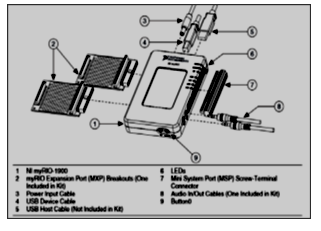
Figure 1: NI MYRIO-1900 and accessories [14].
3.2. Advantages of ZYNQ Board:-
For cost and Power Reduction, Zynq can combine the features of several components into a single device. When Zynq chips are purchased in bulk, the versatility of the technology enables consumers to use a single chip for several products, thereby lowering costs. Additionally, there is a significant reduction in power usage as a result of the internal processing of data and computations within Zynq rather than data being transmitted from component to component [15].
System Integration with Programmability, Today’s cutting-edge businesses can integrate many system components into ever-smaller devices all the way down to a single chip owing to the development of technology that has given rise to the system-on-chip (SoC) concept in the electronics industry. Zynq is a revolution in SoC-level integration [16]. It combines the functionality and power characteristics of an ASIC, the adaptability of an FPGA, and programming simplicity connected to microprocessors into a single device. A 2-chip solution is less dependable and less secure than Zynq because it is a fully integrated system.
Heightened system performance, which distinguishes Zynq from competing products, is the seamless integration of bandwidth between the processing system and programmable logic. This bandwidth is several orders of magnitude larger than what a 2-chip system would be able to provide. As a result, programmers can create accelerators with speeds up to 10 times faster for specific processes [16].
3.3. Why was LabVIEW Chosen?
LabVIEW is a system design tool that employs mathematically based textual and graphical programming techniques to design processes using a graphical user interface. Unlike other common programming methods, LabVIEW includes high-level devices that simulate various communication components and generate various waveforms. In addition, LabVIEW can store data in reports and connect to a variety of measures and sensors. This software has been extensively employed in several industries, including telecommunications, aerospace, and medical research. Because of their adaptability and agility, engineers and scientists need to swiftly develop and test new ideas frequently. One of the main benefits of LabVIEW is its capacity to handle enormous volumes of data, which is crucial for many research applications. As an all-in-one solution for various engineering projects, the software also provides a variety of tools for signal processing, data analysis, and visualization. Overall, LabVIEW is a potent tool that may facilitate and accelerate the design of complicated systems for engineers and scientists [17].
4. Material and Procedure
The transmitter data for the LDPC system consists of an LDPC matrix called the parity check matrix. The data were encoded using the parity-check matrix after generation. We modulated using the BPSK technique, after which it was influenced by the AWGN channel and demodulated before passing it on to the decoder, which decoded it using the min-sum algorithm into the original data.
4.1. LDPC Encoding Stage (Generate the parity-check matrix).
The first step: is to generate a parity-check matrix that defines the relationship between input data and parity bits. This matrix is typically sparse and has a low-density structure.
The second step: The input data is converted into a bit sequence, which is then converted into a bit sequence that can be processed by the LDPC encoder.
The third step: The input data are multiplied with the parity check matrix, and the bit sequence is multiplied with the parity check matrix to generate parity bits.
The fourth step: Adding parity bits to the original data: Generated parity bits are added to the original data to create an encoded message.
The fifth step: Transmitting the encoded message: The encoded message is transmitted over a communication channel
4.2. BPSK Modulation and Channel
To modulate the encoded data, it uses BPSK to convert each bit into another modulated bit. It converts ones to negative 1’s. Each zero bit is changed to a positive 1. We take the coded data and then create a loop to generate the modulated data. The AWGN channel model was then used to add Gaussian noise to the modulated data. These modulated data pass through the channel and are corrupted by the AWGN.
4.3. 5G NR LDPC Decoding
The min-sum algorithm is a popular method used in low-density parity-check (LDPC) decoding. It is an iterative algorithm that aims to minimize the sum of the absolute values of the variable node updates during each iteration. The algorithm works by computing the messages sent between variable nodes and check nodes in a bipartite graph representation of the LDPC code.by using LabView “It is one of the most popular engineering software “we can build software for all our system
The implementation of each block is briefly described as follows:
Step 1: The message is generated randomly by using MATLAB, then reading the message from the text file and storing it into a character array to encode all message characters
Table 1: Structure of base graph [19]
| Set index (i) | Lifting sizes (Zc) |
| 0 | 2, 4, 8, 16, 32, 64, 128, 256 |
| 1 | 3, 6, 12, 24, 48, 96, 192, 384 |
| 2 | 5, 10, 20, 40, 80, 160, 320 |
| 3 | 7, 14, 28, 56, 112, 224 |
| 4 | 9, 18, 36, 72, 144, 288 |
| 5 | 11, 22, 44, 88, 176, 352 |
| 6 | 13, 26, 52, 104, 208 |
| 7 | 15, 30, 60, 120, 240 |
Step 2: Fill the base graph by selecting one of the existing Base Matrices. Base Graph (Base Matrix.There are 102 codes derived from only two base graph matrices by lifting each with every one of the 51 lifting sizes. There are two types of base graphs for the 3GPP standard. The first, BG 1, had 46 rows and 68 columns. The second is BG 2, which has 42 rows and 52 columns. The choice between them was based on the coding rate and size of the information bits. To get the size of information bits, you should know the value of the lifting size (Zc). For each base graph, there are various values for lifting sizes ranging from 2 to 384 [18].The maximum number of information bits can be calculated using the following formulas, depending on the number of base graphs.
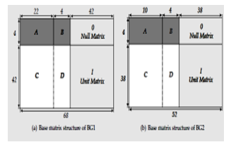
Figure 2: Region division and parameters of base matrix [19].
Step 3: converting Base graph into parity check matrix
Parity Check Matrix: The Parity check matrix was built from the base graphs. Each element in the base graph is replaced by a Zc × Zc matrix. This replacement depends on the value of each element and applies the following rules:
- If the value of the element is (-1), then the Zc × Zc matrix is a matrix of zeros.
- If the value of the element is (0), the Zc × Zc matrix is an identity matrix.
- For each other values, the Zc × Zc matrix will be an identity shifted matrix with the value of the number
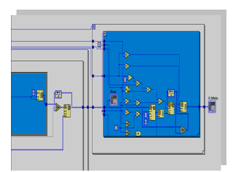
Figure 3: LABVIEW Implementation of H Matrix from block diagram
- Load base graph using read delimited Spreadsheet.vi block.
- Loop each element in the base graph and check the value of this element.
- Develop a corresponding Zc × Zc matrix for each element.
- The developed matrix is rotated to correct the parity-check matrix.
Step 4: Adding parity bits to the messages bits to encoding its.
The main goal of LDPC encoding is to add parity bits to the messages bits. The addition of parity bits to each code block increases the reliability of sent data to develop the code word. The code word is the encodeddata used to transfer it from the transmitter to the receiver.Assume we have an M vector that represents the massage bits donated by M1, M2, and M3… Mk. And the parity bits in the P vector which donated by P1, P2, and P3… Pn. The code word C is created by concatenating these two vectors which is following that: . To confirm that the encoding stage has been done successfully, we should apply the next equations: And Then developing the parity check matrix following its rules. After that, you could get the parity bits by using this formula: [20]. Finally, the code word is generated easily by adding the parity bits to the information bits [20].
Step 5: Recover the original data
Min-Sum Algorithm (MSA). A block diagram is shown below represents the implemented system.
- Initialize specified array called this array contain both variable nodes and check nodes.
- Any non-zero elements in is equal to its relative non-zero elements included in the received data (transmitted data after channel).
- Start to loop every row in with the maximum iteration value.
- Calculate the log of every row and its sign by multiply all signs for each row.
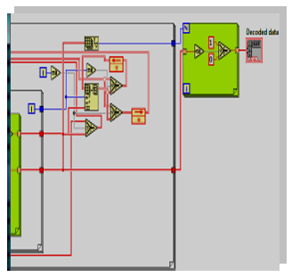
Figure 4: LABVIEW Implementation of 5G-LDPC Decoder
Step 6: Performance testing stage
This section presents the iterative decoding performance of our LDPC codes with different iterations. For the LDPC code, we chose the LDPC code with a code length of 1360 bits and a code rate of 0.5. The min-sum decoding algorithm is used for the LDPC codes, and the maximum number of iterations is set to 30 because it is sufficient for the convergence of the decoding algorithm. The simulation was performed under an AWGN channel with a BPSK constellation. It should be noted that, to verify the performance of the product codes, we notice that we achieve increased coding gain of our system.
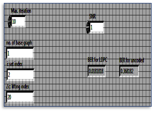
Figure 5: Output of the BPSK in LABVIEW with and without LDPC
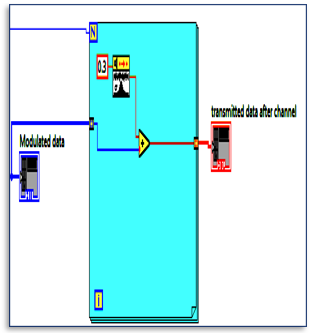
Figure 6: LABVIEW Implementation of transmitted data after channel
We repeat this operation about five times with a different value of SNR. The result was recorded for the LDPC coding data and the uncoded data. The results show the relationship between bit error rate (BER) and signal-to-noise ratio (SNR).For LDPC-coded and uncoded data, when SNR increases, It indicates that the BER is decreasing on a fast track. However, the BER rate for un-coded data is still high, although the SNR has increased. The Min-sum decoder was finished by the LabVIEW FPGA, and a successful compilation was necessary to burn the program onto a Zynq plate card.
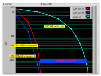
Figure 7: LABVIEW Implementation of BER vs. Eb/No with LDPC
5. The performance of the proposed method by MATLAB
Simulation outcomes are predicted using BER values compared to signal-to-noise ratio values. Our system is written in MATLAB to get the estimated relationship between BER and SNR. Figure 8 shows the relation between BER and SNR in MATLAB. Performance of 5G LDPC code with BG1, BG2, un-coded for code rate of 1=2, code word length of 1360 bits for the min-sum algorithm for the proposed system. The simulation results shown that, we achieves about 6.0dB coding gain. Estimating the Bit Error Rate and Sigma system. The simulation results show that we achieve about 6.0 dB of coding gain. Estimating the Bit Error Rate and signal-to-noise ratio involves a number of variables. Where the anticipated value of the seed is no more than 4. As a result, the following table, Table II, shows a comparison of the performance of the output with and without LDPC code. The Noise Ratio involves a number of variables. Where the anticipated value of the seed is no more than 4. As a result, the following table,
Table 2: Shows a comparison of the performance of the output with and without LDPC code
| parameters | NO LDPC |
With LDPC [20] |
Our proposed |
| n | 100 | 200 | 1360 |
| m | 50 | 100 | 440 |
| Seed in | -1 | -2 | -2 |
| EB/NO | 5.2 | 6.18 | 2.38 |
| Max. iteration | 30 | 30 | 30 |
Table 2 show that LDPC codes perform more effectively when comparing resource usage and Eb/No with a variety of LDPC encoder and decoder parameters. Our proposed LDPC achieves small SNR value.
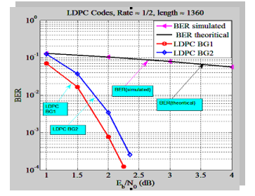
Figure 8: Show that relation between BER & SNR by MATLAB
5.1. FPGA Scheme
- On the PC, install the drivers for the NI yRIO-1900 device and the FPGA module.
- The “create project” button is pressed after the LabVIEW program has opened. The “MyRIO custom FPGA project” option is then chosen on the newly opened interface.
- The project name and MyRIO connection method are chosen.
- .Content is added to the project’s main folder at the designated location.
- Next, choose “New VI” from the context menu when you right-click on “FPGA Target” in the next Figure interface. This will add a new VI to the “FPGA Target” section [21]. The block diagram and VI’s front panel will also be shown. The gadget is set up in accordance with the chipset.
- The LabVIEW project will be saved with the registered name once it has been developed in the VI. The project is eventually completed. As a result, the
- FPGA in the NI MyRIO-1900 device is set up in accordance with the chipset.
Figure 9: FPGA scheme creation interface
Figure 9 shows what the program looks like on my device where This research, it is thoroughly taught how to develop an FPGA project using the LabVIEW program and load it into the FPGA chip on any target device. The NI MyRIO-1900 was chosen as the study’s target device
6. Second method For LDPC Implementation by Using HDL Design
6.1. 5G-NR Encoder Synthesis And Simulation Result
The 5G-NR LDPC system is individually described in Verilog. The different modules in the LDPC system design are designed by the Vivado 18.2 Schematic tool
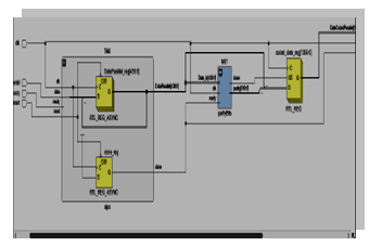
Figure 10: RTL of the Encoder
Figure 10 shows that The RTL for LDPC encoder for constraint length 1360 and bit rate 1/2 has been developed and synthesis is done shown that the resulting shapes from synthesis on LDPC encoder.
- The following table show that the Encoder hardware resources utilization.
Table 3: Encoder Hardware resources utilization.
| Resource | utilized | Available |
Utilization
|
| LUT | 390 | 70560 | 0.55 |
| FF | 596 | 141120 | 0.42 |
| IO | 3 | 82 | 3.66 |
| BUFG | 1 | 196 | 0.51 |
Table 3 displays specifics regarding the utilization of the hardware resources. It provides data on the number of slices, flip-flops, LUTs, IOBs, global buffers, and BUFG
The following simulation shows how input is provided to the encoder once the data read assertion has been made and how the encoder is asserted following the completion of the encoding operation. The LDPC encoder yields meaningful results, as demonstrated in Figure 11
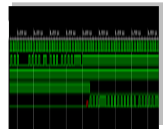
Figure 11: Simulation results of the Encoder output obtained from Vivado simulation.
We notice that the output stat appears after 4.400 ns. The channel sends the coded bits to the decoder after encoding. There are no errors in this simulation. It is possible to observe the asserted control signals for each as shown in Figure 11.
6.2. 5G-NR Decoder Synthesis And Simulation Result
The following Shape shows the process of decoding. This figure shows that the input is entered in parallel. The same thing appears in the output, which also appears in parallel. It shows that 14 bits appear in one microsecond.
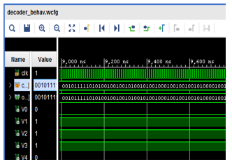
Figure 12: Simulation results of the decoder output obtained from Vivado 18.2
A shown in Figure12 that the simulation output from the decoder, if we compare the data input of the LDPC encoder shown in Figure 11 with the output of the LDPC decoder decided in Figure 12, it is shown that the NRLDPC decoder perfectly estimates the original data. Considering the effect of noise, if the encoded data is corrupted, then the decoder should also be able to retrieve the original message sequence. The decoder can detect and correct the errors with excellence.
7. Device utilization reports
It was shown that the resulting shape from the synthesis of the architecture was placed and routed in a ZYNQ FPGA with the highest speed grade (-2) using Vivado 18.2 from Xilinx. The following shown is the part from circuit of the LDPC decode.
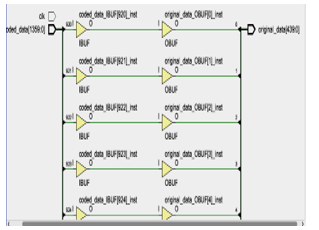
Figure 13: RTL of LDPC decoder unite
Figure 13 shows that The RTL LDPC Decoder for constraint length 1360 and bit rate 1/2 has been developed and synthesized.
All architectures were synthesized, placed, and routed in a kit FPGA with the highest speed grade (-2) using Vivado 2018.2, The ZYNQ (xczu3eg-sbva484-1-e) was chosen to build the system using Vivado 2018.2 program, as shown in Table IV below.
Table 4: Hardware Decoder Utilization for Our Proposed Design
| Resource | Utilized | Available | Utilization |
| LUTs | 159 | 70560 | 0.28 |
| LUTRAM | 58 | 28800 | 0.20 |
| FF | 2275 | 14112 | 1.61 |
| IO | 4 | 82 | 4.88 |
| BUFG | 1 | 196 | 0.51 |
7.1. Timing and power summary
- Speed grade: -2
- Minimum period: 30.3035 ns
- Maximum frequency: 33 MHz
- Minimum input arrival time before the clock: 1.245 ns.
- Maximum output required time after the clock: 0.809 ns
8. Comparative Analisa is between Various Fpgas Devices
It shows that from our proposed implementation, we have an area overhead reduction of more than 50% compared to referenced designs, and we can achieve more than 21000 LUTs compared with other designs LUTs, where other designs consume more FFs and BRAMs. Furthermore, it has much higher throughput (224 vs. 87 and 5 MB/s). So ZYNQ’s (xczu3eg-sbva484-1-e) FPGA is better than previous state-of-the-art solutions in terms of area. Moreover, the implemented 5G NR LDPC decoder was tested against an additive white Gaussian noise channel (AWGN) and consequently has gained more and more popularity in many applications. The frequency of the 5G NR LDPC decoder obtained is 33 MHZ with a minimum period of 30.3035 ns. The main limitation of the implemented decoder appears to be small lifting factor values. For them, it is necessary to freeze the decoder for several clock cycles during one iteration to provide enough time for Check message memories to update. This reduces the decoder’s throughput and power. The Vivado tool reports a total on-chip power of 5.897W. After Making a comparison between our results with another LDPC architectures in[22], [23], and [24]. In [22], used the Xilinx Kintex-VII architecture. In [23] used an FPGA, a Xilinx Virtex 7. In [24] Xilinx Kintex Ultrascale FPGA.
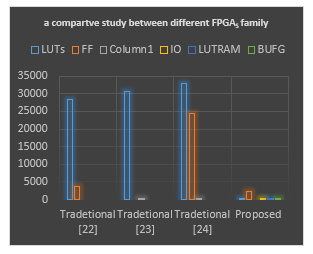
Figure 14: Show that a comparative study between Implementation results using different FPGAs family kits
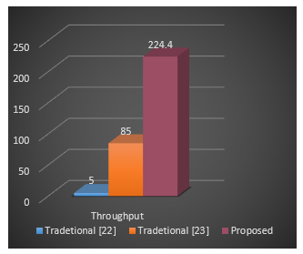
Figure 15: Performance comparison of Throughput consumption
Our proposed implementation is done using ZYNQ Xilinx Ultrascale (xczu3eg-sbva484-1-e). However [23] has a better throughput value than [22], architecture resources have been very high according to throughput value. Our proposed implementation has 38.77% improvement rate in throughput than [23]. On other hand, [24] consumes 137.5 BRAM which is very high. But In our implementation, we replaced the BRAMs in [24] with 58 LUTRAMs. Our implementation progress is due to the proposed architecture. This method saves the resources that are used for converting the base graph to the parity check matrix. The architecture of ZYNQ Ultrascale allows the parallelism of the design in order to increase throughput. So, we notice that if we look at the table as well, we will find that our proposal is to save power, and this is the best thing in modern systems, which is to save power. Our implementation provides saving resources utilizations compared to other designs.
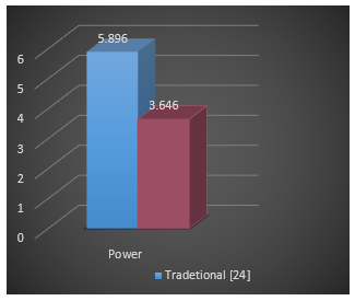
Figure 16: Performance comparison of Power consumption
In Figure15, it shows the difference between our proposed design and [24]. The design we introduce saves about 2.251 mW. This is a regular result when using less resources.
9. Conclusion
5G-NR LDPC decoding is the best technique for decoding codes. In this work, an area overhead reduction has been achieved compared with respect to previous work at the same code rate. 5G-NR LDPC decoders with constraint length 1360 and code rate 1/2 have been successfully implemented on the Virtex-6 FPGA NI MY RIO Zynq-1900 device of the NI family and realized using Xilinx Vivado 18.2. The MIN-SUM algorithm is employed in wireless communication to decode the 5G-NR LDPC codes; those codes are used in every strong digital communication system. We have implemented an area-optimized VLSI architecture for the 5G NR LDPC Encoder and 5G NR LDPC Decoder. The 5G NR LDPC decoder allows safe data transmission via error correction, and the original message can be recovered accurately. This proposed 5G NR LDPC algorithm presents a reduction in power and cost and, at the same time, an increase in processing. Speed. 5G-NR LDPC code has better performance than other LDPC codes, especially at low Eb/N0 values. This means we save on power. Furthermore, it is much better if we compare the un-coded performance. This is besides enhancing throughput. Among the advantages of LDPC is that, by increasing the number of iterations, the performance is enhancedmore and more. In this work, area and power overhead reductions have been achieved compared with reference works at the same code rate. Field Programmable Gate Array (FPGA) technology is considered a highly configurable option for implementing many progressive signals. In future work, we will try to improve the latency of the LDPC decoder.
Conflict of Interest
The authors declare no conflict of interest
- G. Suchitra, “Performance Analysis of Ldpc Code in Digital Communication System Using LabVIEW,” Hindusthan Journal of Information Communication and …, 1(1), 11–18, 2020.
- J. Xu, Z. Zheng, K. Tian, “Low-Density Parity-Check Codes: Research Status and Development Direction,” Journal of Information Security, 13(04), 257–271, 2022, doi:10.4236/jis.2022.134014.
- K. Huo, Z. Hu, D. Liu, Design and Implementation of Shared Memory for Turbo and LDPC Code Interleaver, Wireless Communications and Mobile Computing, 2022, 2022, doi:10.1155/2022/5782199.
- A. Devrari, A. Kumar, A. Kumar, “FPGA Performance Analysis of LDPC and Turbo Codes for Communication System,” 2022.
- M. Pregara Zachary Saigh Advisors, I. Soo Ahn Yufeng Lu, “Low Density Parity Check Code Implementation Senior Project Final Report Students,” 2013.
- A.A. Ovchinnikov, A.A. Fominykh, “Decoding of LDPC codes for 5G standard using source distribution,” 2020 Wave Electronics and Its Application in Information and Telecommunication Systems, WECONF 2020, 0–4, 2020, doi:10.1109/WECONF48837.2020.9131454.
- K.W. Jensen, Polar Codes and LDPC Codes in 5G New Radio.
- M. Indoonundon, T. Pawan Fowdur, “Overview of the challenges and solutions for 5G channel coding schemes,” Journal of Information and Telecommunication, 5(4), 460–483, 2021, doi:10.1080/24751839.2021.1954752.
- V.L. Petrović, D.M. El Mezeni, A. Radošević, “Flexible 5g new radio ldpc encoder optimized for high hardware usage efficiency,” Electronics (Switzerland), 10(9), 2021, doi:10.3390/electronics10091106.
- L.Y. Hosni, A.Y. Farid, A.A. Elsaadany, M.A. Safwat, “5G New Radio Prototype Implementation Based on SDR,” Communications and Network, 12(01), 1–27, 2020, doi:10.4236/cn.2020.121001.
- G.M.G. Madhuri, A.V.K. Sravanthi, A.R. sri, G.S. Mrunalini, G.S. Kumar, “Implementation of Decoder Using Ldpc Codes on Fpga,” International Journal of Engineering Applied Sciences and Technology, 04(12), 354–357, 2020, doi:10.33564/ijeast.2020.v04i12.062.
- D.S. Lenin, H. Shekhar, “Design and Implementation of Optimized LDPC for SDR Applications,” … Journal of Engineering, Management, & Applied …, 1–10, 2021, doi:10.14456/ITJEMAST.2021.15.
- J. Nadal, A. Baghdadi, “FPGA based design and prototyping of efficient 5G QC-LDPC channel decoding,” Proceedings of the International Workshop on Rapid System Prototyping, 2020-Septe, 2020, doi:10.1109/RSP51120.2020.9244853.
- U. Guide, “NI myRIO-1900,” 1900.
- M. Ali Altuncu, T. Guven, Y. Becerikli, S. Sahin, “Real-Time System Implementation for Image Processing with Hardware/Software Co-design on the Xilinx Zynq Platform,” International Journal of Information and Electronics Engineering, 5(6), 473–477, 2015, doi:10.7763/ijiee.2015.v5.582.
- A.A. Rafiq, M. Yusuf, Pujono, “Implementation of Digital Image Processing Using NI myRIO and Arduino Mega 2560 as Controller on Rover Bogie Robot,” Proceedings – 2018 International Conference on Applied Science and Technology, ICAST 2018, (March 2020), 210–215, 2018, doi:10.1109/iCAST1.2018.8751506.
- S. Mhaske, H. Kee, T. Ly, A. Aziz, P. Spasojevic, “FPGA-Based Channel Coding Architectures for 5G Wireless Using High-Level Synthesis,” International Journal of Reconfigurable Computing, 2017, 2017, doi:10.1155/2017/3689308.
- L. Wang, “Implementation of Low-Density Parity-Check codes for 5G NR shared channels,” Degree Project Computer Science and Engineering, 2021.
- Y. Tian, Y. Bai, D. Liu, “Low-latency qc-ldpc encoder design for 5g nr,” Sensors, 21(18), 2021, doi:10.3390/s21186266.
- P. Fang, “Application Analysis of Low Density Parity Check Code for Wireless Network,” IOP Conference Series: Earth and Environmental Science, 634(1), 2021, doi:10.1088/1755-1315/634/1/012043.
- E. Y., H. Çıtak, M. Çoramık, “A FPGA Project with MYRIO,” International Advanced Technologies Symposium, (December), 19–22, 2017.
- A. Verma, R. Shrestha, “A New Partially-Parallel VLSI-Architecture of Quasi-Cyclic LDPC Decoder for 5G New-Radio,” in 2020 33rd International Conference on VLSI Design and 2020 19th International Conference on Embedded Systems (VLSID), IEEE: 1–6, 2020, doi:10.1109/VLSID49098.2020.00018.
- J.C. Liu, H.C. Wang, C.A. Shen, J.W. Lee, “Low-Complexity LDPC Decoder for 5G URLLC,” Asia Pacific Conference on Postgraduate Research in Microelectronics and Electronics, 2018-Octob, 43–46, 2018, doi:10.1109/PRIMEASIA.2018.8597812.
- A. Katyushnyj, A. Krylov, A. Rashich, C. Zhang, K. Peng, “FPGA implementation of LDPC decoder for 5G NR with parallel layered architecture and adaptive normalization,” Proceedings of the 2020 IEEE International Conference on Electrical Engineering and Photonics, EExPolytech 2020, 34–37, 2020, doi: 10.1109/EExPolytech50912.2020.9243997.