A Circuit Designer’s Perspective to MOSFET Behaviour: Common Questions and Practical Insights

Adv. Sci. Technol. Eng. Syst. J. 8(4), 41–59 (2023);
 DOI: 10.25046/aj080406
Metal Oxide Semiconductor Field-Effect Transistors are commonly taught in courses for electrical engineers as they are the most common components within integrated circuits. However, despite numerous papers and books on MOSFETs, students still struggle with understanding their behaviour, particularly in the saturation region. This paper presents an expanded explanation of MOSFET behaviour, with a consistent and causal derivation of Level 1 MOSFET behaviour from a few equations, aimed at students without an extensive technological background. The paper provides illustrative explanations to help them understand MOSFET behaviour and addresses common students’ questions, such as why the current is limited by charge carriers in the semiconductor substrate and why characteristic curves do not follow a parabolic curve in saturation. In addition to providing a comprehensive introduction to MOSFET behaviour from a circuit designer’s perspective, this paper also offers valuable insights into interpreting AC parameters in modern MOSFET models. These parameters are often key to understanding and solving circuit problems related to small signal behaviour and frequency response, as demonstrated through various industrial application examples. These examples highlight how to bridge modern MOS models, such as the BSIM model, with MOS-Level 2 modelling, which is easily interpreted by users. By presenting these real-world examples, analysed by a symbolic analysis tool incorporating the BSIM to Level 2 AC model, this paper provides a practical and accessible approach to teaching MOSFETs and their applications in industry.
1. Introduction
This paper is an extension of the contribution presented at the International Conference on Synthesis, Modelling, Analysis and Simulation Methods, and Applications to Circuit Design (SMACD) conference [1]. The extension includes a comprehensive introduction and technological considerations before deriving the current equations consistently, making them easily understandable for undergraduate students and addressing frequently asked questions. The motivation for this paper were the discussions with students in a Metal Oxide Semiconductor Field-Effect Transistors (MOSFET) fundamentals course in 2019 – it became clear that they often struggle with understanding the behaviour of MOSFETs in the saturation region. Specifically, they frequently ask for a simple explanation of why the current is limited by charge carriers in the semiconductor substrate and why the characteristic curves do not follow a parabolic course in saturation. To aid in their understanding, many analogies have been used, such as “students as electrons” rushing in and out of a lecture hall through doors or buses transporting people from one location to another. However, these analogies have failed to adequately explain the behaviour, and often, lecturers resort to citing additional effects that are not described or are parasitic in nature. In fact, a simple explanation of the Gate-channel capacitance fixing the number of charge carriers by Q = CV and the inability of charge carriers to switch polarity for not further following the parabola can logically answer both questions. Surprisingly, students told that even lectures held by technologists failed to provide satisfactory answers to these questions.
The industrial application examples have also been expanded, demonstrating how to bridge the gap between modern MOS models such as the Berkeley Short-channel Insulated Gate Field-Effect Transistor Model (BSIM) and MOS-Level 2 modelling that is easily interpretable for the user. This approach in combination with symbolic circuit analysis based on computer algebra [2] can solve even industrial-related circuit problems related to small-signal and frequency response behaviour.
Field-Effect Transistors (FETs) are one of today’s fundamental electronic devices whose basic idea is to change the conductivity of a system by the influence of an electric field. The fundamental operating principle of a surface field-effect transistor was first proposed by Lilienfeld ([3], [4] and [5]) and Heil [6] in the early 1930s. Subsequently, Shockley and Pearson [7] studied this idea in the late 1940s. After the first device-grade Si-SiO2 system was realized by Ligenza and Spitzer in 1960 by thermal oxidation [8], Atalla proposed the basic MOSFET structure based on the Si-SiO2 system [9]. As a result, the first MOSFET was reported by Kahng and Atalla in 1960 [10]. A complete breakdown of the historical development of the MOSFET can be found in [11] and [12]. For the technology, application and device physics, reference can be made to [13] – [16].
The MOSFETs are themselves subdivided into a wide range of sub-categories. In the following, only the most widespread semiconductor technology for integrated circuits, the MOS technology (based on silicon), will be discussed. Hierarchically, the MOSFET is found as a subgroup of the MISFET, which in turn can be classified under the IG-FET. The abbreviations stand for:
- MOS … Metal / Oxide / semiconductor,
- MIS … Metal / insulator / semiconductor and
- IG … insulated G
In general, FETs are used with a MIS-structure. Replacing the insulator by silicon dioxide (SiO2) one obtains the MOS-structure with SiO2 being the Oxide. This type of insulation is preferred because oxides are characterized by the fact that they have a high dielectric strength, which should ideally be infinite in an insulator and also because they increase the Gate capacitance (high relative permittivity κ or εr), the importance of which will be discussed later in this paper, without increasing the leakage currents. The insulated Gate significantly reduces the power consumption of the FET (only leakage current flows into the Gate). In addition to oxides, the Gate insulation can also be technologically realized using other materials such as silicon nitride, polymers or a combination of different materials, as in the Metal Nitride Oxide semiconductor FET (MNOSFET). Therefore, MOSFETs are to be considered as a subgroup of MISFETs.
MOSFETs can be used in a wide range of applications due to their favourable characteristics. These include applications such as: analogue switching, high impedance amplifiers, microwave amplifiers and digital circuits (complementary MOS, abbrv. CMOS). Among the most appealing features of a MOSFET are significantly higher input impedances (compared to a bipolar junction Transistor, abbrv. BJT), negative temperature coefficient at high current levels, and the absence of forward-biased pn-junctions. The high input impedances are a result of the Gate insulation, which make them particularly suitable for standard microwave systems. Because of the negative temperature coefficient, the current drops as the temperature rises, resulting in a uniform temperature distribution across the device and preventing thermal runaway and breakdown. A MOSFET is thus thermally stable even in a parallel connection. Due to the lack of forward-biased pn-junctions, minority charge carrier storages cannot form. Between two switching states, unlike BJTs, MOSFETs do not have to compensate for stored charges resulting from diffusion tails, the cause of which is the average lifetime of minority carriers, allowing them to achieve much higher large-signal switching speeds. In addition, MOSFETs can be operated as a constant current source due to their nearly constant current-voltage characteristics in the saturation region. This property is particularly exploited in integrated circuit (IC) technology in the form of diode-connected MOSFETs, e. g. for operating point adjustment or current mirrors.
In the following, this work focuses only on the conventional Bulk (long-channel) MOSFET, i. e., no Silicon on insulator (SOI) MOSFETs or MOSFETs with multiple Gate electrodes are considered.
2. Ease of Use
First, the general structure of a MOSFET must be clarified. For this purpose, Figure 1 shows the typical structure of an n-channel MOSFET, which has three or four terminals: Gate (G), Source (S), Drain (D) and Bulk (B). The controllable current flow occurs between the Source and Drain by manipulating the channel by varying the Gate-Source voltage, which allows the current through the transistor to be selectively influenced according to the current-voltage characteristic. The individual terminals are contacted with regions or semiconductive layers that are diffused into the substrate. Starting from the bottom terminal, the MOSFET Bulk consists of a p-type (PMOSFET: n-type) silicon single crystal, and Source and Drain are formed by two n+ regions (PMOSFET: p+). The latter represent reservoirs for the charge carriers that would be minority charge carriers in the substrate. For this reason, like a BJT, a MOSFET can also be modelled by two antiserially connected diodes.
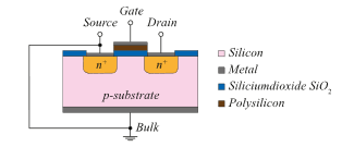
Figure 1: Conventional Bulk NMOSFET – General Structure
In contrast to the BJT, the Gate (analogue BJT: base) of a MOSFET is deliberately so wide that the space charge zones of the Source-substrate- and substrate-Drain- pn-junctions do not overlap. Thus, there is no transistor effect as with a BJT. For a voltage VGS < Vth, one of the two pn-junctions (Source-substrate or substrate-Drain) on the Source-Drain path is always reverse biased, i. e., one of the two diodes is reverse biased regardless of the polarity of VDS.
The “+” sign of the n+ respectively p+-areas means that these are heavily doped with impurity dopants. In most cases, the Gate in NMOSFETs is n+-type polysilicon. As the name implies, it is not a Si-single-crystal but rather an imperfect crystal with a large number of grain boundaries. The Gate insulator is typically made of a thin SiO2 layer. In stand-alone MOSFETs the Bulk is internally connected to Source to generate a common reference potential. Current can flow between Source and Drain, when a voltage with the correct polarity (i. e., + at the Gate pin) is applied between Gate and Source.
3. MOS-Structure
The heart of a MOSFET is formed by the MOS structure, which is obtained by omitting the Source and Drain regions of the conventional Bulk MOSFET. The substrate is often, as within this paper, given by silicon. Silicon is in the 4th main group in the periodic table of the elements proposed by Dmitri Mendeleev. According to Lewis and Kossel (1916) [17], a chemical bond is particularly stable when the nearest electron gas configuration is reached (noble gas rule). With an electron configuration of: [Ne] 3s2 3p2, silicon is still missing four electrons in the 3p-orbital to the next noble gas: Argon [Ne] 3s2 3p6 (octet rule). Consequently, a Si atom in an (infinitely extended, i.e. no edges) silicon crystal forms four covalent bonds to the neighbouring Si atoms. Thus, next noble gas configuration is achieved, and the Si crystal is chemically stable. As mentioned before, the p-Bulk MOS structure, as used in NMOSFETs, consists of a Gate electrode (typically n+ poly-Si), the Gate-Oxide as insulator (or dielectric as explained later) and a p-type substrate (Si Bulk) with a doping concentration NA. The subscript “A” stands for “acceptor”, since p-type doping means the intentional implantation of atoms with less valence electrons than Si into the Si single crystal of the substrate (e. g. boron, B, 3rd main group in the periodic table). Accordingly, the full four bonds to the neighbouring Si atoms in the crystal cannot be formed. As a consequence, the dopant atom is ionized (atomic body is negatively charged), and it provides a free-moving (diffusion processes in the semiconductor crystal) hole to the semiconductor structure. An explanation of the concept “hole” is given in Section 5.
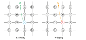
Figure 2: Silicon Crystal Structure with n and p Doping
In the ionized state the dopant atom is called an “acceptor ion” because the underlying atomic body has an affinity for electrons, i. e., the atomic body strives to compensate for the hole and achieve charge neutrality towards the outside. In contrast, an n-Bulk MOS structure of PMOSFETs consists of the Gate (typically p+ poly-Si), the Gate-Oxide, and the n-type Si substrate with a doping concentration ND, where the “D” stands for “donor”, since atoms with more electrons than Si (like phosphorus, P, 5th main group in the periodic table) are incorporated into the Si single-crystal upon n-doping. With five valence electrons, phosphorus can form five covalent single bonds, unlike silicon. However, since only four neighbours are available for a potential bond in the semiconductor crystal lattice, the pentavalent phosphorus is also ionized (atomic body is positively charged). As a result, the crystal lattice has one free-moving electron (diffusion processes through the crystal lattice) available for charge transport. This is also the reason why these ions are called “donors”. Figure 2 is intended to illustrate these relationships.
Because the Bulk contact is assumed to be grounded, the voltage drop across the MOS structure VGB is equal to the applied potential at the Gate VG, as shown in Figure 3. In the following, electrical potentials shall be labelled with only one letter in the subscript, e.g., VG for the Gate potential, and voltages (potential differences) with two letters, for example VGS for the Gate-Source voltage. Important for the voltages is the arrangement of the letters. The first letter indicates the start potential, and the second letter indicates the end potential, which makes the voltage arrow VXY go from potential VX to potential VY (according to the way of speaking). Therefore, the following relationship between voltage and potentials applies: VXY = VX – VY.
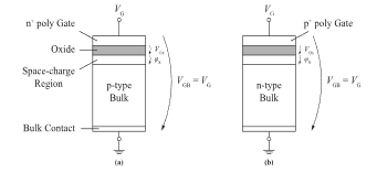
Figure 3: Two-Terminal MOS Structures. (a) p-Bulk MOS. (b) n-Bulk MOS. (adapted from [18]).
To derive the equations and gain a deeper understanding of the operating principle of the MOSFET, the type of transistor used must be specified. In this work, an n-channel transistor is taken as a model, since the NMOS is the standard model in lectures. The derivations and analysis can be performed analogously for a p-type, although some properties must be considered vice versa. This is due to the analogue but inverse MOS structure of the PMOSFET. This means for a PMOSFET, all voltages enter the equations with reversed polarity. In addition, the electrons contribute significantly to the charge transport (current flow) in an NMOSFET and the holes in a PMOSFET.
From a technological point of view, further insight into the physics of the MOS structure can be obtained by means of the energy band diagram. Figure 4 shows the energy band diagrams of the separated components of a NMOS structure under equilibrium conditions, i. e., Gate potential VG = 0. The vacuum energy Evac was chosen as the reference energy level. Each of the three regions has its own electron affinity χ, which is defined by the difference between Evac and the conduction band lower edge EC, and a work function ϕ, which results from the separation between Evac and the Fermi energy EF. Due to of the high n-doping of the Gate, the Fermi level is slightly above the conduction band edge EC. The electron affinity is the same for both the Gate and the Bulk since both are Si, χSi.
The work function in the Gate ϕG corresponds approximately to the electron affinity χSi, which can be explained by the high doping. In the Bulk, the work function ϕB depends strongly on the Bulk doping NA. The insulator (SiO2) is characterized by the high band gap EGox (gap energy EG = difference between conduction band lower edge EC and valence band upper edge EV).
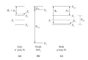
Figure 4: Energy Band Diagrams of the individual (separated) Components of a p-Bulk MOS Structure. (a) Gate (n+-poly Si). (b) Insulator respectively Oxide (SiO2). (c) Substrate (p-Bulk). (adapted from [18]).
When the three individual components are brought together (galvanic contact) to form a MOS structure and the equilibrium state is considered with no externally applied voltage (VG = 0), the Fermi level of all three regions must be aligned in the same vertical position (same energy level) throughout the entire structure. To achieve this condition, the band diagram of the Bulk material can be held fixed at the contact points to the Oxide, while the rest of the structure can be pulled down until the Fermi energies EF in the Bulk material and poly-Si match. This process results in band bending of the conduction and valence bands and of the intrinsic Fermi level Ei. To obtain a correct energy band diagram, the following points should be noted:
- In the substrate, the bands are bent only near the surface, i. e., the Si / SiO2 interface, while far away from it the band relations remain unchanged. This is also the reason why the contact points to the Oxide should be held fixed during the band displacement.
- The relations between valence and conduction bands remain unchanged compared to the case where all three regions were separated.
- The intensity of the bending of the valence and conduction bands as well as the intrinsic Fermi level Ei are identical.
- Since the doping level of the poly-Si is so high, the bands at the Gate-Oxide interface bend only to a very small extent, so they can be neglected in the following.
The final band diagram of a p-Bulk MOS structure is shown in Figure 5 (a). The reason for the band bending is the work function difference between Gate and substrate (Bulk). To eliminate band bending, i. e., to make the bands flat, a certain voltage must be applied to the Gate. This specific voltage is called flat-band voltage VFB. Note that for a p-Bulk MOS structure, VFB is negative and for n-Bulk structures it is positive.
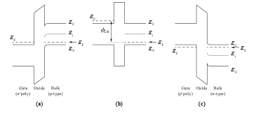
Figure 5: Band Diagrams of different MOS Structures. (a) p-Bulk MOS at VG = 0.(b) p-Bulk MOS at VG = VFB (c) n-Bulk MOS at VG = 0
(adapted from [18]).
Another important parameter in MOS theory is the surface potential φS, which is related to band bending.
![]()
Here φi is the electrostatic potential introduced in Appendix B (cf. (31)) and y is the spatial coordinate in the direction of the perpendicular of the semiconductor surface (i. e. into the depth of the substrate). Therefore, the origin of the y-axis lies in the Oxide / substrate interface and is often referred to as the surface.
4. States of the (N)MOS Structure
To gain a deeper understanding of the operation of an NMOS structure (p-Bulk), the effects of different applied Gate voltages are first investigated. Throughout this analysis, the term “surface” (subscript: “S”) is used to reference the interface between the Oxide (insulator) and the substrate (strong band bending). In contrast, the term “Bulk” (subscript: “B”) is used to indicate that the analysis is performed far away from the interface, i. e., deep inside the substrate (little to no band bending). Additionally, all the different cases will be considered with a Source-Drain voltage equal to zero, VDS = 0. In total, four relevant states can be identified:
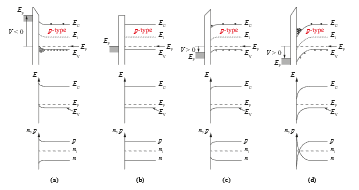
Figure 6: Band Diagram (top), Carrier Concentration (middle, Ordinate has log-scale) of Si Substrate for a p-Bulk MOSFET. (a) Accumulation, VG < 0. (b) Flat-band Case, VG = VFB. (c) Depletion, VG > VFB. (d) Onset of strong Inversion, VG > Vth. (modified taken from [18] and [19]).
Note, that from now on only the interior of the substrate is considered, with x = 0 being the interface between Oxide / substrate resp. Oxide / Bulk.
- VG < 0 resp. φS < 0 (Accumulation case)
A sufficiently large negative voltage at the Gate (in relation to the Source) causes the energy bands to bend upwards near the substrate surface. This leads to a negative surface potential, φS < 0. Now the surface majority carrier (in case of a p-substrate (NMOS): holes) concentration pS is larger than the Bulk majority carrier concentration pB, and the surface minority carrier concentration nS is smaller than its corresponding Bulk value nB.
Within circuit technology and digital computing technology (CMOS circuit technology) this condition has no further meaning: In analogue circuits, MOSFETs are used primarily as amplifiers, and their behaviour is largely determined by the relationship between the input and output voltages and currents. Hence, most circuits operate in the saturation region, only a few in the linear region, but both require inversion. In digital circuits, MOSFETs are used primarily as switches, and the most important characteristics are their on / off states and the speed with which they can switch between these states. So, the accumulation region has no direct impact on these characteristics, and hence, it is also not relevant to digital circuit design.
- VGS = VFB φS = 0 (Flat-band case)
As the name suggests, the energy bands become flat at a less negative voltage, the flat-band voltage VFB, i. e., the band bendings disappear.
- VGS > VFB φS > 0 (Depletion case)
When the Gate voltage is more positive than VFB, the energy bands near the surface bend downward and the surface potential becomes positive, φS > 0. Thus, the holes are repelled from the surface (diffusion processes), which leads to the fact that only the uncompensated acceptor atomic hulls (ions) remain (firmly bound to the lattice structure of the substrate) and a space charge region is formed.
- VGS Vth (Inversion)
Further increase of the Gate voltage enhances the depletion, i. e. nS increases, pS decreases and the thickness of the space charge region increases further. Once nS equals pS, the type of conductivity near the surface goes inverted. Consequently, in an NMOS with a p-substrate, the depletion region changes from p-conducting to n-conducting. This is called the onset of weak inversion. With the Gate voltage so large that the surface electron concentration is as high as the Bulk hole concentration, nS = pB, the onset of strong inversion is initiated. Now a channel (for NMOS: n-channel) is formed, which allows an effective current conduction. In other words, with the onset of inversion, the resistance of the channel is reduced. In addition, due to the local charge reversal, the effect of the antiserially connected pn-junctions (diodes; Source-substrate and substrate-Drain) is suppressed.
Note that the threshold voltage Vth is one of the most important electrical parameters of MOSFETs. It is defined as the Gate voltage that triggers the transition of the transistor from the off-state to the on-state. Because there is no uniform definition of the transition between the off-state and the on-state, several definitions of the threshold voltage are in use. In the Appendix A one can see the different definitions [18]. The authors restrict themselves within this publication to definition “Constant current”.
As soon as the Gate voltage VGS exceeds Vth, a conductive channel is established. If the complete MOSFET, as shown in Figure 1, is now considered, a Drain current ID can flow through the channel region. Therefore, the state of inversion is also called on-state and all other cases with VGS < Vth are called off-state. These terms originate from CMOS circuitry (digital logic).
5. Transition Process in the MOS Structure from the OFF-State to the ON-State
Within the off state, according to the mass action law
![]()
with n being the electron concentration, p the hole concentration and ni the intrinsic charge carrier concentration, a very temperature- and doping-sensitive charge carrier equilibrium is established, which is shown externally by the electrical charge neutrality. If the voltage between Gate and Bulk or Source (internal connection) is now increased so that the Gate receives a positive voltage, the charge carriers in the p-doped silicon shift. Electrons are increasingly drawn from the substrate below the interface between substrate and insulator (Oxide), which in turn causes the positive “charges” (holes) to be displaced from this region via diffusion processes into deeper substrate layers. It is important here that the electrons from the substrate do not leave it. Nor can they do so since the Gate is insulated by the Oxide. The phenomenon of displacement can be attributed to the effect of the electric field that builds up between the substrate and the Gate metallization. The result is the formation of a Gate-channel capacitance, with the Oxide acting as a dielectric.
Looking at (20), which will be explained in more detail in Section 8, it can be seen that the Drain current ID, i. e. the current to be controlled, also depends on the Gate capacitance Cox. Accordingly, with an increase in Cox, an increase in ID can be achieved. To enhance Cox further, the insulator layer thickness was reduced in semiconductor technology. However, this caused several new problems with increasing miniaturization. On the one hand, the maximum field strength before an electric breakdown was reduced and on the other hand, the leakage currents increased drastically due to the tunnel effect. To ensure that Cox can still be increased, and the insulator layer does not become too thin, the trend is toward high-k materials. The artificial word “high-k” is composed of the adjective “high” and the letter “k”. The “k” refers to the Greek letter kappa κ, which is the symbol used in English-speaking countries for relative permittivity. High-k materials (e. g. hafnium dioxide) are mainly used because they have a higher dielectric constant (relative permittivity εr), allowing for a thicker dielectric resp. insulator (Oxide) layer without compromising the device’s performance. This helps reduce Gate leakage current, improving the device’s power efficiency, and Gate tunnelling current, improving the device’s switching speed. In contrast, low-k materials are used to reduce parasitic capacitances in interconnects but are not used for the dielectric layer of very small MOSFETs due to their low dielectric constant. This is the reason why the permittivity of the Gate insulator has been increasingly addressed in recent years.
In the following, the Gate capacitance will be modelled as a plate capacitor with negligible edge effects. This insight gives rise to two explanations for the electron accumulation at the surface:
- Equivalent charge principle:
Based on this principle, there are always the same number of charges (charges are always quantized) with opposite sign on the two electrodes of a capacitor. Therefore, if positive charges accumulate on the Gate electrode due to the positive (NMOS) Gate potential (conception: “suction” of free electrons from the e. g., highly doped poly-Si), negative charges (electrons) must accumulate at the interface between Oxide and substrate due to the Gate channel capacitance. Otherwise, the electrical charge neutrality of a capacitor cannot be preserved. Accordingly, the number of charge carriers which can accumulate at one electrode is limited by the other electrode (in this case the applied electrode voltage potential) and a proportionality constant which is impressed by the capacitance.
- Influence:
With the “suction” of the electrons from the Gate electrode, the charge balance (neutrality) is disturbed in such a way that a positive centre of charge is formed. Since equal charges always repel each other (keyword: Coulomb or electrostatic forces), the conceptual “positive” charges (holes) are displaced into deeper substrate layers, leaving the negative charges (electrons). In addition, electrons are drawn out of the substrate under the interface via the same forces.
In an NMOS, the electrons in the p-substrate are the minority charge carriers while the holes are the majority charge carriers. Since the accumulation of electrons near the substrate / Oxide interface now occurs due to the above reasons, the holes within the interface are filled up by neighbouring places of the lattice. The consequence of the enrichment with electrons is noticeable by the depletion layer forming at the substrate / Oxide interface.
If there is a further increase in the Gate-Source voltage, the threshold voltage Vth is exceeded, and inversion comes into picture. Under these conditions, so many electrons are locally accumulated that the electrons become majority charge carriers. Thus, more electrons accumulate locally than the doping of the p-substrate can compensate. Because of the locally limited accumulation, the inversion is also locally limited. The so-called charge reversal starts. Incorrectly, it is often also referred to as a doping inversion, but this is wrong in the context of doping, since – in the case of an NMOS – there are no donor ions in the substrate. On the contrary, only acceptor ions can still be found in the p-doped substrate. The charge reversal in an NMOS creates a continuous, low-resistance n-conducting channel, which disables the function of the pn-junction between the n-doped islands and the substrate. Consequently, a current can now flow between Drain and Source: ID. The channel region is only as large as the inversion zone and isolated from the substrate (channel: n-surplus, substrate: p-surplus) due to further pn-junctions forming (i. e. diodes in blocking direction). It follows that the MOSFET is voltage controlled, which makes it fundamentally different from the BJT, which is current controlled. Now it also becomes apparent where the terms NMOS and PMOS come from. The N and P refer to the conductivity of the forming channel. This is characteristic for the respective type of MOSFET, because an NMOS with an N-channel would immediately compensate all holes or positive charges due to the accumulation of electrons within the channel region and would therefore be non-conductive for these “positive” charge carriers. However, the electrons allow other electrons to pass. The opposite is true for the PMOS. Accordingly, the PMOS also requires a negative voltage at the Gate to form a p-type channel. At this point, a further difference can be identified in comparison to the BJT, since only one charge type contributes to the transport of the current depending on the substrate type. Therefore, the MOSFETs belong to the unipolar transistors and not to the bipolar transistors.
At this point it should be additionally noted that this is only a model, i. e., holes are not actual charge carriers, such as electrons or positrons. Holes are crystal lattice defects, where an electron is missing at the respective lattice place (e. g., consequence of doping with trivalent boron). This defect is interpreted as a conceptual positive “charge”. Hence, holes cannot move by themselves. Instead, their mobility results from diffusion effects. For example, an electron from a neighbouring lattice place can fill up the vacancy (hole), creating a new hole at the lattice point where the electron came from. The electron has, so to speak, “jumped” one place further in the lattice. One can imagine this process as “wandering of the holes”.
6. Deriving the MOSFET Equations (NMOS)
After explaining the individual states of the MOS structure, analytical equations describing the NMOSFET properties in the on-state (i. e., strong inversion case) are derived below. As mentioned above, the Gate-Source voltage causes to form a capacity between the substrate underneath the Gate and the Gate electrode, whereby – due to the positive potential at the Gate – electrons are attracted towards the Gate. The attracted and accumulated charge carriers create an induced n-layer. This yields a complete n-region from Source to Drain, i. e., a channel which forms kind of a low resistance tube where electrons can go from the Source electrode to Drain electrode. Thereby, the resulting electron flow builds up the desired current ID through the MOSFET. A further increase of the Gate-substrate voltage attracts more electrons underneath the Gate and a higher current can be achieved. But why is the current limited by the Gate-substrate voltage and the number of electrons attracted from the p-substrate to forming the channel?
Looking at the MOSFET from a circuit-theoretic perspective, the MOSFET can be modelled as a voltage controlled current source (VCCS) as the Gate-substrate voltage resp. the Gate-substrate capacity influences the current between Source and Drain.
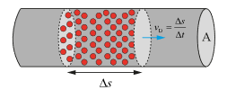
Figure 7: Electrons within a Conductor
The number of charge carriers N being stored in the tube shown in Figure 7 can be calculated using the equality
![]()
where n is the charge carrier density, A the cross-sectional area of the “tube” and Δs describes the way passed by the electrons in each Δt. Multiplying the cross-sectional area A with the way passed Δs gives the volume VTube in the second part of (3). The current through the MOSFET can be obtained by partially differentiating the charge by the time, i. e.
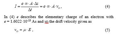
The drift velocity is composed of the mobility µ and the electric field E applied to the tube.
7. Deriving the Current in the NMOS
The derivation of the current in the channel of a MOSFET is based on the Gate-channel capacity. This capacitance is the linchpin of the explanation of the saturation or limitation of the current: The electrodes of the “capacitor” are formed by the Gate on the one hand and the electrons in the channel underneath the Gate-Insulator on the other hand. It is important to mention that the electron layer, also called inversion layer, is in contact with the Source and the Drain at the same time (cf. Figure 8)
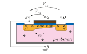
Figure 8: MOSFET with channel (NMOS)
The potential difference within the channel (and therefore the inversion layer) is determined by the potential difference between Source and Drain. The emerging capacity between Gate and channel can be modelled via the equation The real mathematical description of the charge within the Gate-channel capacity has a slightly shifted outcome as the threshold voltage Vth needs to be considered, since significant conductivity of the channel only occurs when this voltage is exceeded.
As previously indicated, the Gate-channel capacitance will be modelled as a plate capacitor with negligible boundary effects. The simple equation for the capacitance design applies. Adapting (6) to the current case gives
![]()
where VGC represents the voltage across the Gate channel capacitance and ε = ε0 ∙ εSiO2 the permittivity of the Oxide (insulator) layer. The area A describes the area covered by the Gate-insulator and can be approximated as
![]()
using the Gate width W and its length L, where length refers to the distance between the Source and Drain pn-junctions. We assume, as can be seen in Figure 8, that the channel length is equal to the Gate length. In reality, the effective channel length is assumed to be a little less than the full channel length. This is due, for example, to the fact that the ion implantation of the n+ regions of the Source and Drain contacts cannot be focused precisely, resulting in a slight underdiffusion under the Gate (but still in the substrate), which leads to a reduction of the actual effective channel length. The thickness of the Oxide (distance between the Gate and substrate) is described by the parameter dSiO2 which is called TOX in Simulation Programs with Integrated Circuit Emphasis (SPICE).
As the capacitance is nearly constant, the number of charge carriers is enforced by the Gate-Source voltage (equivalent charge principle) and, hence, limited (Q = C·V). Thus, it cannot be further increased by charge carriers from the battery.
To determine the current characteristic, the voltage V(x) underneath the Oxide is introduced that varies between VS = 0 und VD = VDS as the Source potential is set as the reference potential. Therefore, the charge is also a function of the location x. If the voltage VGS is not considered from the point of view of the Gate, but from the point of view of the channel, i. e., the counter-electrode, then due to the principle of equivalent charge, the voltage is reversed. Due to this, the voltage VGS in the substrate points from Source to Drain and V(x) is oppositely directed. In the next step, to determine the channel voltage at a certain location x, all voltages can be superimposed according to the superposition principle. Thus, the Gate channel voltage VGC is composed of the difference between VGS in the substrate and V(x). Considering the infinitesimally small area
The negative sign is due to electrons being the charge carriers in an n-channel MOSFET. As a preparation for the integration to get the Source-Drain current an essential case study must be executed: linear region and saturation region need to be looked at separately. The essential argumentation for these two regions is that the voltage term
![]()
may never get negative or change its sign because otherwise the sign of the charge dQ would be reversed and the electrons being the charge carriers would suddenly become positrons.
It is also possible to look at the energy of a capacitor which cannot become negative, too. The current
![]()
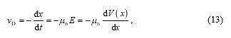
flows against the direction of travel of the electrons. Their speed is described by the drift velocity vD. Henceforth, it shall be additionally assumed that the electron mobility in the channel is constant and does not depend on the electric field in the x-direction. Mobility reduction due to the vertical electric field will not be considered here. This assumption works well for long-channel MOSFETs, but accuracy is reduced, especially when considering nanometre MOSFETs, since constant mobility and thus a linear velocity-(electrical)field characteristic is assumed throughout the entire device. This is remedied by the two-region MOSFET model, which will not be discussed here, but can be looked up in [18]. The minus sign is a consequence of the direction of the electric field, which points from Drain (positive potential) to Source (negative potential; grounded), where the electrons flow in the opposite direction. It is additionally noteworthy that the mobility μn is not the substrate mobility, but the effective mobility, which is explained in more detail in Appendix C.
Since – as already mentioned in the introduction – this work is restricted to long channel MOSFETs, the longitudinal field along the channel is not sufficient to achieve a charge carrier saturation velocity. Under these circumstances, the velocity is coupled to and limited by the mobility (and thus within this model constant). Otherwise, the short-channel effects explained in more detail in [18] would have to be considered.
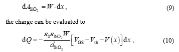
Using (12) and differentiating (10) regarding the time the differential equation for the current ID,
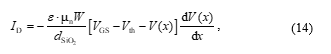
can be obtained. Equation (14) can be solved by integrating from 0 to L along the channel and from VDS to 0 because of the voltage directed in reverse to the flow of electrons. Changing the integration variable by multiplying (14) with dx the voltage V(x) can be replaced by V as the integration incorporates solely the voltage difference and no longer the location along the channel.
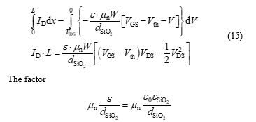
The factor is called K’ or KP, whereby the fraction (without the mobility µn) is called (effective oxide capacitance per unit area).
Looking at the Drain current ID it is clear to see that the characteristic curve has a quadratic behaviour at the beginning (cf. Figure 10). The distribution of the charge carriers in the channel has an approximate triangular shape (at least shown in many textbooks, e. g. [20]), which forms the channel, as the electrons are pulled stronger towards the Drain the higher the Drain-Source voltage VDS is. At the peak point of the characteristic curve, that is when the current does not sink but remains nearly constant.
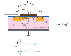
Figure 9: NMOSFET with Pinch-off
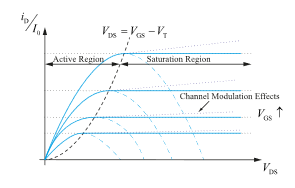
Figure 10: ID as a Function of VGS and VDS
This peak is the point where the so-called Pinch-off takes place. No more charge carriers can reach for the Drain. If the Drain-Source voltage is further increased the length of the Pinch-off region varies in a way that only a certain amount of charge carriers can reach the Drain. The remaining electrons recombine as minority charge carriers with the holes in the p-substrate. Here one finds the missing arguments in most of the books and lectures: There is no inversion regarding the polarity of the charge carriers nor negative energy can be stored on a capacitor ((10), (11)). The resulting voltage for the current respectively the charge carriers remains constant. This is the explaining argument clarifying the trouble of the students in understanding the saturation region, and why it does not follow the parabola (15) after its peak (cf. Figure 10, blue dashed line).
![]()
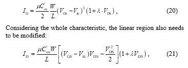
If VDS ≤ VGS – Vth (15) shows a linear correlation with VGS. This section of the characteristic curve is therefore called linear, ohmic or active region. When VDS > VGS – Vth = VDS,Sat the voltage term in (15) needs to be set to VDS = VGS – Vth = VDS,Sat. The equation for ID in the saturation region can then be evaluated to
![]()
The current ID stays nearly constant (regarding this model approach) and has a quadratic dependence on the Gate-Source voltage VGS, which can be perfectly modelled by a VCCS. The quadratic dependence on VGS can be seen in Figure 10 as the distances between each blue curve within the saturation region are not uniform.
Within the device, the Pinch-off effect can be thought of as follows:
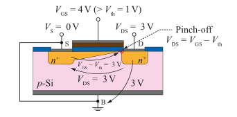
Figure 11: Calculation Example for the Superposition of the Voltage in the Substrate
The Pinch-off effect within the MOSFET device is a result of voltage drops within the substrate. This effect is illustrated by a small calculation example, where the voltage drops superpose within the substrate, thereby affecting the shape of the channel. This calculation example is only intended to illustrate the facts of the voltage drops and is by no means an accurate model. However, as can be seen very well, two voltages overlap within the substrate. Firstly, the one which is impressed by VDS from Drain to Source and secondly, the one which drops due to the principle of equivalent charge between the interface substrate / Oxide and Source. The latter goes from Source to substrate / Oxide interface, since for an NMOS VDS > 0 applies and thus the other plate of the plate capacitor (corresponding to the modelling of the MOS structure) must be negatively charged and thus the Source potential VS = 0 V is larger. Consequently, the two voltages are oriented oppositely. They cancel each other out exactly when VDS = VGS – Vth is fulfilled. This point is the so called “Pinch-off point”, which occurs when there is a reduction in the relative voltage between the Gate and the substrate, as explained and shown in Figure 11. The point marks the x-coordinate at which the channel is pinched off and the strong inversion changes into a depletion zone. If the Drain voltage VDS is now further increased (above VDS,sat) at constant Gate voltage (VGS = const.), the voltage drop from the Drain to the Source in the substrate predominates. As a result, the channel tends to be pinched off even sooner with respect to the x-coordinate. For VDS > VDS,sat, the Pinch-off point moves closer to the Source, but the voltage at the Pinch-off point remains the same at VDS,sat. So, the saturation voltage is the voltage at which just such a channel and thus the strong inversion still exists in the substrate. This voltage cannot change with a fixed Gate voltage VGS, since the charge carriers in the channel (minority charge carriers with respect to the substrate) are determined by the MOS capacitance Cox – as already explained in the derivation. Thus, the total number of charge carriers (proportional to the overall charge) in the channel cannot change (otherwise the charge neutrality would be violated), whereby also according to Q = C·V with C = Cox = const. and Q = const. the voltage drop, that needs to be compensated for the onset of saturation (channel Pinch-off) by the Drain-Source voltage, cannot change.
In summary, the Pinch-off phenomenon in MOSFETs is influenced by the interplay between the Gate-Source and Drain-Source electric fields. The Gate-Source field creates the channel, while the Drain-Source field causes a voltage gradient along the channel that directly affects the electron concentration in the substrate. When VDS is small and VG > Vth is fulfilled, the Drain-Source electric field is relatively weak, and the channel remains uniformly populated with electrons. As VDS increases, the Drain-Source electric field becomes stronger, leading to a reduction in electron concentration near the Drain region (cf. Figure 12). When the Drain-Source field becomes strong enough to oppose the Gate-Source field at the Drain end, the channel is pinched off, and the transistor enters the saturation region. Beyond the Pinch-off voltage, the channel’s resistance increases, and the Drain current ID remains relatively constant despite further raise of VDS.
It is important to note that as the Drain potential VD increases, the voltage drop from the Drain to the Bulk also increases due to the internal connection of Source and Bulk. Consequently, the space charge region and the area of influence of the depletion induced by the Drain-pn-junction increase on the Drain side. This enlargement of the space charge zone results in more occupiable states for the same number of minority charge carriers, leading to a decrease in charge carrier density on the Drain side. Thus, the area of strong inversion (channel) decreases. Figure 12 shows the described situation, where the wedge-shaped region marks the area of strong inversion, where depletion comprises the area where more minority charge carriers are present than in the Bulk. Sufficient minority carriers are also present outside the strong inversion, i. e., in the depletion region, where most of the substrate majority carriers are compensated. Therefore, in the saturation region, the Drain current can still reach the Drain-side n+-island. However, the electrical resistance within the depletion zone is higher than that within the local inversion (conductive channel). Thus, within the saturation, the resistance that the electrons “see” increases as they flow through the substrate from the Source to the Drain region (physical current direction). This shows on the one hand, why the current does not abruptly drop to zero and on the other hand, why the current remains almost constant within the saturation. Due to the constant voltage VD,sat, the number of charge carriers arriving at the Pinch-off point remains the same. Consequently, despite the reduction of the effective channel length from L to L’, approximately the same current ID flows. Only if the shortened amount of the effective channel length is a substantial fraction of the channel length, an increase in the Drain current can be observed. As the channel length is reduced, the electric field in the channel increases, which causes the depletion region to expand towards the Source. This expansion reduces the effective length of the channel, and the Pinch-off voltage also reduces. As a result, the Drain current increases as the channel length decreases, assuming the voltage between the Source and Drain remains constant. This effect is considered within the channel length modulation in a more detailed model description, as discussed in the next section.
In summary to understand the difference between Pinch-off voltage and threshold voltage, the Pinch-off voltage is the voltage at which the depletion region around the Drain meets the depletion region around the Source, causing the channel to be “pinched off” and the Drain current to saturate. It is also sometimes referred to as the saturation voltage VDS,sat. On the other hand, the threshold voltage is the voltage at which the MOSFET just starts to conduct current, with the channel beginning to form under the Gate. It is the minimum voltage required at the Gate to induce a channel and allow current flow between the Source and Drain. Hence, the threshold voltage Vth refers to the Gate-Source-voltage and Pinch-off voltage VDS,sat refers to the Drain-Source-voltage. They can be seen in the equations that describe the device’s behaviour, such as the Drain current equation. In the saturation region, the Drain current is essentially independent of the Drain voltage and is limited by the Pinch-off voltage. As mentioned before, this effect is particularly exploited in integrated semiconductor technology, since the MOSFET resembles a current source within saturation, i. e. almost constant current over a wide voltage range. Both voltages are important parameters in the MOSFET model and are influenced by various, such as the Gate-Oxide thickness and the doping concentration of the semiconductor material.
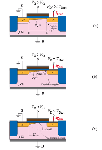
Figure 12: MOSFET operated (a) in the linear Region, (b) at Onset of Saturation, and (c) beyond Saturation (reduced effective Channel Length) with technical Current Direction. (taken from [19])
8. A more accurate Modelling of the Characteristic Curves
The ideas developed beforehand aimed to provide an easy derivation and intuitive understanding of the MOSFET characteristics. Another important parameter that has not been discussed so far is the threshold voltage Vth. It describes the Gate-Source voltage from where the inversion layer is built up and a significant current flow starts.
Using the equality (Shichman-Hodges resp. Level 1 model; no consideration of device random noise (thermal and flicker), sub-threshold behaviour, and high frequency effects)
![]()
With Vth0 as zero threshold voltage, γ as the body effect parameter, and ϕF as the Fermi potential remaining constant, when the semiconductor is in balance. The zero-threshold voltage is the value of the threshold voltage Vth when VBS = 0, i. e., the substrate has Source potential. The Fermi potential is the energy at which the Fermi-Dirac distribution has the value 1/2. Since this energy corresponds directly to a distribution function, it is (in very simplified terms) a measure of the number of free-moving charge carriers in semiconductor and is strongly influenced by the doping.
Equation (19) reveals an influence of the Bulk-Source voltage VBS on the concrete value of the threshold voltage Vth. Consequently, the threshold voltage varies as a function of the Bulk-Source-voltage. This effect is commonly referred to as the “body effect”. In the small-signal model (cf. Figure 19, Figure 20, Figure 24), this must be taken into account (Bulk-control). As mentioned before, usually the Bulk-potential is set to a fixed value (e. g. ground) or connected to Source, which reduces or compensates the body effect. It allows further control of the transistor and is especially important in integrated circuit technology. Less commonly, through hole technology (THT) MOSFETs also have the Bulk terminals pulled out of the package as a fourth pin.
Another important effect within the MOSFET and the Shichman-Hodges model is the channel-length modulation (CLM). Increasing the Drain-Source voltage over the value of VDS,sat = VGS – Vth causes the Pinch-Off inducing a reduction of the effective channel length and therefore raises the current. Modelling the rising current when the Drain-Source voltage increases can be done with the channel length modulation factor λ. Within an empirical model, λ results from the common intersection point of the voltage axis and the extensions (tangents created in the saturation region) of all branches in the output characteristic field (ID as a function of VGS).
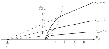
Figure 13: Channel Length Modulation, Asymptotes in Saturation Region meet at the Point of Early Voltage.
Using the intercept theorem, the equation for the characteristic curve of the MOSFET in saturation region can now be written as
Typically, λ has a value of 0.05 V-1. λ induces an rDS in the alternating current (AC) model. The effect on the characteristics of the MOSFET resulting from the channel-length modulation can be compared with the Early effect in bipolar transistors. However, their origins are different, which is why they are not identical.
Up to now, only the case where VGS > Vth has been considered analytically for NMOSFETs. In this range, the presented model works very well, but it lacks accuracy for Gate-Source voltages smaller than Vth. When this condition is met, only a very small Drain current ID (not zero) flows. This is called the subthreshold regime. For the Drain current in the subthreshold regime of an NMOSFET, a rather long derivation, which will not be explained in detail here but can be found in reference [18], results in the following expression:
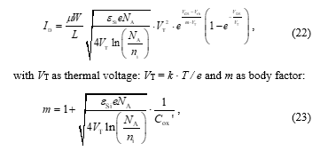
Because of the resulting impractical expression, a new widely used parameter has been introduced to characterize subthreshold MOSFET behaviour: sub-threshold slope S. This emerges from (22) assuming VDS >> VT, since under this condition the last exponential term converges to zero. S is then defined as the derivative of the logarithm of ID with respect to VGS.
The unit of S is typically given as mV/dec. The subthreshold slope gives an indication of how much the Drain current varies as a function of the Gate-Source voltage. For example, if S is given as 100 mV/dec and the Gate voltage is changed by 100 mV, the subthreshold Drain current will change by a factor of 10, i. e., a decade. The theoretical lower limit of S is 60 mV/dec, since an ideal case of m = 1 would then be encountered. In addition, it should be noted in the considerations that the equations only yield ideal values, since, for example, short-channel effects are neglected. These effects will not be discussed further in this paper. However, [18] can be cited as a suitable source for further reading.
What has also not been discussed in the previous MOSFET models are parasitic resistances. So far, it was always assumed that the voltages VGS and VDS applied to the external terminals are equal to those appearing at the intrinsic transistor. However, in reality there are series resistances between the intrinsic transistor and the external terminals, since the Drain current that flows through the channel must also pass through the Source and Drain series resistances RS and RD. These are caused, for example, by path resistances of the Drain and Source regions or contacting resistances. This leads to parasitic voltage drops, which is why the voltages across the intrinsic transistor are usually lower than the voltages applied to the terminals. The relationship between the external voltages (subscript: “ext”) and the internal voltages (subscript: “int”) are given by:
The resistors have only a negligible effect on the MOSFET current-voltage characterization (I–V-characteristic) below the threshold voltage, i. e., in the subthreshold region. In contrast, in the on-state, i. e., beyond threshold, they lead to reduced Drain currents compared to the ideal case of the intrinsic transistor. This effect of reduced Drain current in the on-state can play a substantial role in nanometre MOSFET. For this reason, one of the design goals is to minimize RS and RD. In addition, this reduces the thermal losses of the transistors, which is why this can also be quite relevant for circuit design.
9. Models for Computer-aided and manual Analysis
Analog circuit designers are continuously facing the challenge to squeeze as much performance out of their circuits as the underlying semiconductor technology permits. Pushing a circuit topology to its technological limits requires extensive knowledge of previous designs and deep insight into both the intended functional behaviour of the device under construction and the parasitic effects that degrade its performance. Since conventional numerical circuit simulators cannot provide qualitative insight into the functional dependencies between circuit parameters and behavioural characteristics, it is often necessary to perform a manual analysis of the circuit. At the end of such an analysis the goal is to get an understanding of how the circuit works by interpretation of the mathematical (symbolic) expressions. In this context, the most important application for symbolic (manual) analysis is to gain design knowledge about undesired circuit behaviour observed in numerical simulations, e. g., in the form of resonance effects and instabilities due to parasitic poles or poor power-supply rejection behaviour.
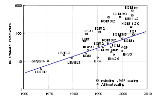
Figure 14: Evolution Model Parameters for MOS Transistors. (taken from [21])
For a fully comprehensive description of the internal operation of a MOSFET to be possible, three-dimensional complete quantum mechanical and atomistic simulations would be required. Since this currently seems unattainable due to a lack of computational resources, various device engineers and researchers have developed simplified abstract MOSFET models with different levels of complexity over the past decades. Because the share of CMOS chips is the largest, a lot of effort has been put into the modelling of MOSFETs, especially pushed by semiconductor manufacturers. Today, models (e. g., BSIM) with several hundred parameters are not uncommon (cf. Figure 14).
On the other hand, designers do not think in the BSIM, especially for the small-signal behaviour as shown in Figure 21. To gain insight into the operation of the circuits, many analogue designers use (15) or (18) for Direct Current (DC), since these equations describe the static behaviour of the MOSFET. Here, the fundamental transistor function of forming and controlling the channel current is modelled. As mentioned above, from a circuit point of view, this model can be represented by a VCCS. However, the dynamic behaviour is neglected and remains unconsidered. This can be remedied by inserting additional internal capacitances. The most important capacitances of a MOSFET and their summary (on the right) are shown in Figure 15.
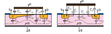
Figure 15: Sectional View of the MOSFET with the most important Capacitances, summarized on the right.
It should be noted that the effect of the individual capacitances is largely dependent on the operating range in which the transistor is located. For example, voltage-dependent capacitances can be defined depending on the Gate-source voltage VGS (cf. Figure 16).
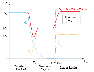
Figure 16: Compilation of the qualitative Capacitance Curves as a Function of the Gate-Source Voltage VGS.
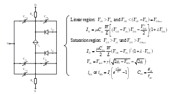
Figure 17: MOSFET Model with the static large-signal Equations.
With additional consideration of the pn-junctions from the Source or Drain to the Bulk, which are abstracted to junction diodes, as well as the terminal resistances, a complete (dynamic) large-signal equivalent circuit can be assembled (cf. Figure 17).
For example, after the operating point has been found using the large-signal equivalent circuit diagram, which roughly corresponds to the SPICE Level 1 model (cf. Figure 18), circuit engineers are then interested in the behaviour of the circuit when excited with signals of small amplitude and power. This is referred to as small-signal behaviour. The corresponding equivalent circuit diagrams can be derived from the large-signal model.
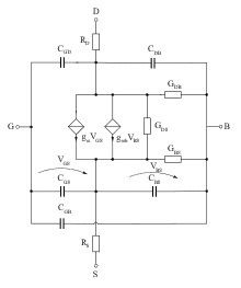
Figure 18: SPICE MOSFET Level 1 small-signal Model.
Using most manual analysis, the goal is to obtain good descriptions of the circuit functional behaviour with as little computational effort as possible. For this reason, the SPICE MOSFET Level 1 model is often already far too complex. A possible simplification for manual analysis is shown in Figure 19. In most cases, however, it will find application without gmb, since Source is mostly connected with Bulk, which makes VBS zero and therefore the corresponding controlled current source can be neglected. The transconductance gmb describes the dependence of the Drain current on the Bulk-Source voltage, i. e., the previously explained body-effect.
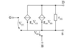
Figure 19: Simple static MOSFET small-signal Model for manual Analysis.
Herby the small-signal quantities are calculated as follows:
Linear / Triode range:
Saturation range:
It is important to note again that most analogue circuit applications are operated in the saturation region because that is where the transistor acts like an almost ideal controlled current source.
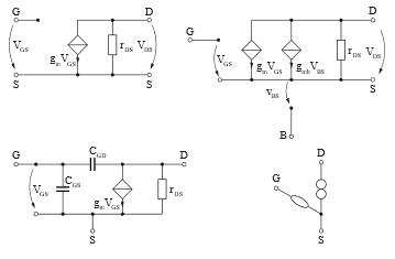
Figure 20: Small-Signal Models for hand calculations.
Other typical small-signal equivalent circuit diagrams may include those shown in Figure 20, including the gm-only, gm–rDS and those extended by parasitic capacitances and/or the Bulk-Source induced gmb if necessary and / or needed. Not well known is the Nullor model in the right lower corner, which is often beneficial and very efficient if dynamic analysis is to be performed.
10. Overview of MOS Models
Accurate modelling of MOSFET devices is critical for the design and simulation of electronic circuits, as well as for the optimization of device performance. Over the years, various MOSFET models have been developed to address the evolving requirements of semiconductor technologies. In this overview, we will discuss the development of MOSFET models, including Level 3, BSIM3, BSIM4, BSIM6, Enz-Krummenacher-Vittoz (EKV), and Penn-State Philips (PSP), highlighting their advantages and disadvantages. [22], [23]
MOS Level 1 to Level 3 are the earliest MOSFET models, utilizing simple equations to describe the basic operation of MOSFETs. The advantages of this model include simple calculations and low computational effort. In this article, we utilize the simpler Level 1 to Level 3 MOS models for a specific purpose: to obtain a straightforward understanding of MOSFET functionality and easily interpretable formula expressions for circuits. This is particularly important in the context of education, where students need to grasp fundamental concepts and relationships. Furthermore, circuit designers also rely on simple and easily interpretable relationships for qualitative circuit explanations, making the use of these basic models valuable in both teaching and practical applications. This is especially the case for small signal and frequency behaviour. However, the model suffers from inaccuracies for modern semiconductor devices, e. g., for short channel lengths and modern process technologies. It should be noted that these inaccuracies mainly refer to large signal behaviour and parasitic effects.
The BSIM3v3 model, specifically version 3.3.0, became an industry standard for accurately describing short-channel MOSFETs down to 180 nm. It accounts for various effects, such as Drain Induced Barrier Lowering (DIBL) that reduces threshold voltage with increasing VDS, short-channel and narrow-channel effects impacting threshold voltage variations, mobility reduction due to vertical electric fields, and velocity saturation. Furthermore, the model considers channel length modulation, weak inversion conduction, parasitic resistances in Source and Drain regions, and “hot electron” effects that influence output resistance and threshold voltage over time.
The BSIM4 model significantly enhances the BSIM3v3 model, offering improvements in various aspects, such as better DC modelling accuracy, improved noise modelling crucial for radio frequency (RF) design, an enhanced capacitance-voltage (C–V) model for a wider range of operating conditions, and a new material model accounting for non-SiO2 insulators, non-poly-Si Gates, and non-Si channels. These advancements make the BSIM4 model more versatile and suitable for modern process technologies and a broader array of applications compared to its predecessor.
BSIM6 is an extension of the BSIM4 MOSFET model and is a charge based symmetric MOSFET model with a charge-based core. BSIM6 has been designed to improve the accuracy of transistor simulations at nanometre scales and to model advanced device structures like FinFETs, nanowire FETs, and double-Gate MOSFETs. Some of the key differences between BSIM4 and BSIM6 include the modelling of carrier-induced voltage effects, addition of symmetry-breaking in mobility models, improved modelling of weak inversion region, and better modelling of back bias dependence. BSIM6 also provides more accurate modelling of sub-threshold slope dependence on Gate length, and improved noise models. Additionally, BSIM6 includes new parameters to capture short-channel effects and improved models for DIBL and threshold voltage roll-off.
The EKV Model was developed for use in analogue and mixed-signal circuits, particularly in submicron CMOS technology. The model accounts for effects such as CLM, substrate resistance, and subthreshold conduction. The advantages of the EKV model include a good compromise between accuracy and computational effort, simpler mathematical formalism compared to BSIM models, and suitability for low-power applications. The model’s disadvantages include not being as detailed as the newer BSIM models, especially for very short channels and cutting-edge process technologies.
The PSP Model is a compact MOSFET model intended for digital, analogue, and RF design, which is jointly developed in the early 2000s by NXP Semiconductors (formerly part of Philips) and Arizona State University (formerly at The Pennsylvania State University). [24] It was designed for improved accuracy, scalability, and predictability for advanced process technologies. The advantages of the PSP model include its physically based nature, good scalability, relatively compact structure, and less complexity than some newer BSIM models. However, the model may not provide the same level of detail as the latest BSIM models.
11. The Crux with the Small-Signal Models
As today’s device models are very complex (cf. Figure 14), such as in the case of BSIM3 or higher, their structure is often based entirely on mathematical considerations instead of the underlying geometrical properties of the device. This makes interpretation of the resulting expressions more difficult, as the BSIM AC models involves transcapacitances (cf. Figure 21), i. e., differentiating VCCS instead of capacitances like CGS.
These transcapacitances, which are based on charge derivatives on the various terminal voltages of the transistor may also become negative. This is difficult to be interpreted and, hence, might be confusing especially if stability problems are investigated being caused by parasitic capacitances.
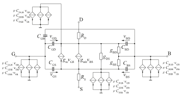
Figure 21: BSIM3 Small-Signal Model with Transcapacitances.
The operational amplifier (artificial term: OpAmp) depicted in Figure 22 is implemented in a 250 nm technology node and BSIM3v3 models were used to analyse its behaviour. The focus of this analysis was to study the sizing of the transistors for obtaining a good operating point and to investigate the AC response based on the small-signal parameters of the circuit.
In Figure 23, the output file provides information about the transcapacitances, which may sometimes exhibit negative values. While in Cadence Spectre, these values are denoted as Cxxxx (e. g., Cbgb), they are represented in Infineon’s in-house simulator Titan as DQxDVyy depicted in the simulator output file in Figure 23. This naming convention represents the charge derivative at x with respect to the voltage yy. This naming is, thus, more informative, as it clearly identifies the transcapacitances as charge derivatives, and reduces confusion for those who may not be familiar with the concept of transcapacitances. It is worth mentioning that the BSIM small-signal models used to extract the transcapacitances are – in contrast to SPICE Level 1-3 – not publicly published, and different simulator providers may have different implementations. For example, some providers use branch-based derivatives, while others use node potential-based derivatives. This leads to the possibility of incompatible parameters between different simulators, adding to the difficulty of physically interpreting the impact of the transcapacitances on the frequency response of the circuit.
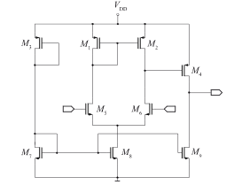
Figure 22: Operational Amplifier in 250nm Technology Node incorporating BSIM3v3 Models.
Despite these challenges, an AC analysis that provides interpretable information about the involved transistor capacitances is important for understanding the performance of OpAmps, especially in advanced technology. This information can help designers understand and adjust the frequency behaviour of their circuits, leading to more optimal designs.
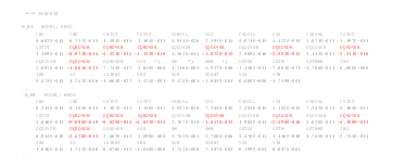
Figure 23: Operating Point and small-signal Parameter Information for the BSIM3v3 MOSFETs (Titan Simulator).
To solve the problem, one can combine the formulas for calculating the SPICE 5-capacitance MOSFET AC equivalent circuit (cf. Figure 24) with the operating points calculated from the BSIM models to obtain reinterpretable capacitances.
However, for a hand analysis, the calculations are too complicated, so the use of a computer program is useful. Thus, such a conversion was implemented for the symbolic analysis tool Analog Insydes [2], which is based on the computer algebra program Mathematica.
Interestingly, it turned out that the SPICE Level 3 equations showed inaccuracies especially in the subthreshold area, so the formulas for the capacitances were revised using the fringing capacitances from Tsividis [16], among others. Fringing capacitances in a MOSFET are parasitic capacitances that occur at the edges of the Gate electrode, where the electric field extends beyond the edge of the physical Gate structure. These capacitances can affect the performance of the MOSFET by increasing the total Gate capacitance, which can impact the speed and power consumption of the device. An important update was the introduction of a partitioning factor (XPART) to distribute Cox between CGS and CGD.
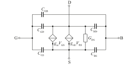
Figure 24: Simplified Level 2 SPICE 5-Capacitance MOSFET AC Model.
To show the steps involved in modifying the SPICE Level 2 5-capacitance MOSFET small-signal model (cf. Figure 24) to match the results of the BSIM small-signal model (cf. Figure 21), an industrial CMOS folded-cascode OpAmp (180 nm technology) is shown in Figure 25, and Figure 26 displays the frequency response of the OpAmp’s open-loop differential-mode voltage gain. Here, the red curve shows the original simulation with the BSIM model, while the green curve shows the AC simulation performed with the SPICE Level 2 AC model, where the parameters were determined from the operating point using the full BSIM model. The agreement is very good for low frequencies but shows a significant deviation for higher frequencies.
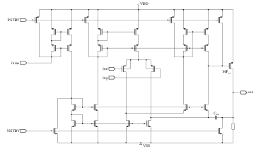
Figure 25: CMOS folded-Cascode Operational Amplifier.
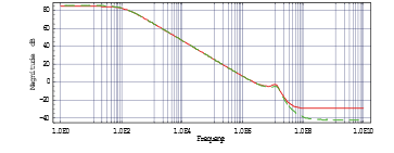
Figure 26: Frequency Response of the OpAmp’s open-loop differential-mode Voltage Gain with BSIM (red) and Level 3-AC Model (green).
The deviation between BSIM model AC simulation and SPICE Level 2 AC analysis becomes even more significant for the power-supply feedthrough (PSF) characteristic in Figure 29 of the amplifier shown in Figure 27 (top-level circuit) and Figure 28 (transistor-level circuit).
Figure 27: Top-level Circuit Schematic.
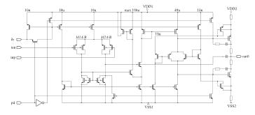
Figure 28: Transistor-level Circuit of the OpAmp with the Power supply rejection ratio (PSRR) Problem.
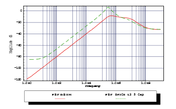
Figure 29: Frequency response of the OpAmp’s power-supply feedthrough (PSF) with BSIM (red) and Level 3-AC model (green).
An analysis of the deviations led to a modification of the underlying SPICE level 2 AC model for the intrinsic Gate-Source capacitance CGS and intrinsic Gate-Drain capacitance CGD for the saturated MOSFET by introducing a partitioning factor XPART for Cox between both capacitances.
Another problem is rooted back to the fact that SPICE Level 2 assumes perfectly pinched-off channel and no fringing capacitances. Hence, fringing capacitances Cif we added to the model in the subthreshold region (cf. Figure 15). Summing up all modifications the following small-signal equations were implemented in Analog Insydes allowing symbolic analysis with interpretable results with an acceptable error.
Sub-threshold region:
Linear region:
Saturation region:
12. Application Examples using the modified SPICE Level 2 Model to solve industrial Circuit Problems in a CMOS Technology requiring BSIM MOS Models
The root cause of many industrial circuit problems is often traced back to their dynamic behaviour, particularly regarding frequency compensation and stability issues. Hence, symbolic extraction of poles and zeros is a crucial aspect of using symbolic analysis in the design of industrial integrated circuits. As designers wanted to understand the cause of the circuit problems it is essential for them to get interpretable results. Resulting in interpretable formulas, which can then be utilized to identify the appropriate frequency compensations for the circuits being analysed. This is achieved by adjusting certain circuit parameters that cause the poles to move in a manner that guarantees stability and eliminates peaking effects in the frequency response, maximizing bandwidth.
The Bode diagram (cf. Figure 26) of the OpAmp shown in Figure 25 displays a prominent peak at approximately 10 MHz, resulting from a pair of parasitic complex poles located close to the imaginary axis. Note, that in the frequency domain complex pole pairs can cause resonance peaks and phase shifts, which can affect the bandwidth and stability of the system. In the time domain, complex pole pairs can lead to oscillatory and damped responses, which can affect the settling time and overshoot of the system. The objective is to extract a simplified symbolic formula for these poles, to identify the components that significantly contribute to the peak. Therefore, it is necessary to shift the conjugate complex pole pair away from the imaginary axis, i. e., either by decreasing the imaginary part or by increasing the real part. The goal is to push the pole into the region bounded by the 45° axes in quadrants 2 and 3 of the root locus plot, cf. Figure 32 (dashed grey lines). The complexity of this issue is evident from the fact that after expanding the model, the netlist comprises of 321 primitive components, leading to a system of 29 × 29 modified nodal equations. Instead of the BSIM3 AC model, the modified SPICE Level 2 AC model was utilized.
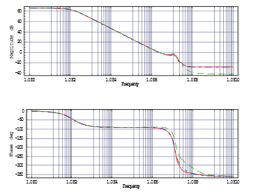
Figure 30: Frequency Response of the OpAmp’s open-loop differential-mode Voltage Gain with BSIM (red) and Level 2-AC Model (green) and modified Level 2-AC Model (blue).
The differential-mode voltage transfer function, shown in Figure 30, has 19 poles and 19 zeros. In its fully expanded symbolic form, it would comprise more than a multitude of 5 ∙ 1019 product terms. Hence, to understand the cause of the peak, the symbolic extraction of the pole pair at s = (–2.1 ± 8.3j) ∙ 107 (with j as the imaginary unit) is essential. To symbolically determine the pole pair, a symbolic approximation algorithm [25] was applied, yielding the following formula:
The formula shows that, given a fixed load CL and operating conditions, an increase in the Gate-Source capacitance of PMOS transistor MP15 Cgs$MP15 will result in a reduction of the pole pair’s imaginary components. It should be noted that altering the compensation capacitance CCO will not affect the resonance peak, as its contribution is in the same order of magnitude in the numerator and the dominator in the square-root expression that yields the imaginary part of the pole pair.
Hence, reducing the imaginary part can be achieved by adding a shunt capacitor between the Gate and Source terminals of MP15 (cf. Figure 31). Figure 32 presents a root locus plot of the amplifier, calculated from the original (unsimplified) system with BSIM models as is varied from 1 pF to 10 pF. The plot confirms the validity of the conclusion drawn from the approximated symbolic pole expression with physical interpretable small-signal capacitance.
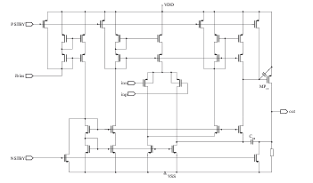
Figure 31: CMOS folded-Cascode OpAmp with Compensation Capacitor derived from symbolic Analysis.
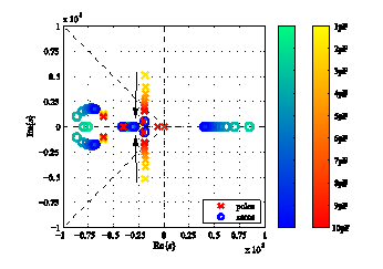
Figure 32: Root locus Analysis of the Voltage Transfer Function as CGS,MP15 is swept from 1 pF to 10 pF.
The second example for the application of Analog Insydes [2] in industrial circuit design using the modified SPICE Level 2 model is the CMOS OpAmp, shown in Figure 25. The circuit operates as an inverting amplifier (in Figure 27).
The AC PSF characteristic of the circuit, depicted in Figure 29, demonstrates an unexpectedly large PSF value of over at 1 kHz frequency, which was predicted to be better than based on rough manual calculations by the designer. PSF occurs when unwanted signals from the power supply source leak into the output of an electronic circuit, hence it is the transfer function from the voltage supply to the output. Power supply rejection ratio (PSRR) is a measure of how well a circuit rejects ripple coming from the input power supply at various frequencies. It is defined as the ratio of the change in supply voltage to the equivalent (differential) output voltage it produces. To identify the reasons for the discrepancy and enhance power-supply rejection, Analog Insydes was again utilized for a symbolic analysis of the circuit behaviour. Solving the unapproximated equations symbolically for the transfer function from VDD to the output node would result in a complex expression with over 1027 terms. Hence, Analog Insydes’ symbolic approximation algorithms are utilized to estimate the PSF behaviour at low frequencies. With an error limit of 10 % at f = 1 kHz, we quickly obtained the following straightforward description of the amplifier’s PSF characteristic, using only a few seconds of central processing unit (CPU) time.
![]()
Additionally, this formula of the PSF can avoid misinterpretation of the real signal flow. The signal path for the PSF is not through the amplifier, but instead, it goes in reverse over the outer feedback resistance R2 to the Bulk of the input pair. The designer neglected these Bulk capacitances in his manual calculations, as he believed them to be insignificant. That also explains that optimizing the OpAmp does not solve the PSF or PSRR problem, and oversimplifying the problem beforehand prevented the true cause of the unwanted circuit behaviour from being discovered. Once the true reason due to (27) was found, introducing a separated well for the input pair, which reduces the influence of the Gate-Bulk capacitance, solved the issue so that the PSF could be reduced. More details on the methodology especially on the generation of approximated symbolic formulas can be found in [25] and [26].
13. Conclusion
The study of MOSFETs is an important part of electrical engineering education as they are the most used components in integrated circuits. Therefore, a systematic and logical explanation of the behaviour of MOSFETs is necessary to facilitate comprehension among students in the context of circuit design. Despite the availability of substantial resources on MOSFETs, students continue to face difficulties in comprehending the concepts of charge carrier limitation and saturation. To address this challenge, a systematic and logical derivation of the Level 1 behaviour of MOSFETs is presented, incorporating simple equations and clear illustrations, to clarify the questions commonly raised by students without adding complexity through the introduction of additional semiconductor effects. Additionally, the use of modern standard MOSFET models, such as BSIM, may also pose difficulties in interpretation. A special problem is rooted back to the fact that – in contrast to the well-known AC models of SPICE Level 1 to 3 – BSIM and PSP small signal models are not published and that they include transcapacitances due to their charge-based modelling instead of physical capacitances. The acquisition of knowledge and insight regarding the behaviour of circuits is imperative for both designing circuits and resolving issues such as instability, ringing and other related phenomena. Symbolic analysis is a useful tool to facilitate this understanding, however, it is important to ensure that the formulas are comprehensible. The utilization of BSIM model and its parameters in conjunction with a modified SPICE Level 3 AC model can help in bridging the divide between technical formulas and their practical interpretation and applications. This methodology can enhance the understanding of MOSFET behaviour and its influence within the circuit design tasks for both students and experienced designers alike.
14. Acknowledgement
We would like to thank Dominik Krauße and Wladek Grabinski for providing valuable material for this contribution as well as Marius Steindel for his support in creating the illustrations and diagrams that helped to clarify and enhance our explanations of MOSFET behaviour.
15. Appendix A
Definitions of the threshold voltage Vth [18]:
Conventionally, the threshold voltage is defined as the Gate voltage that must be applied to the MOS structure to reach a carrier concentration near the substrate-insulator (Si / SiO2) interface that is equal to the majority carrier concentration in the substrate (i. e., far from the interface). In the case of an NMOS with applied threshold voltage and a p-doped substrate, this means that the electron concentration near the interface would be equal to the hole concentration in the Bulk. This condition marks the onset of the strong inversion. In particular, the band bending in the energy band model reaches a value twice as large as the Bulk potential at the location of the interface.
However, this definition is problematic due to the experimental measurement uncertainties of carrier concentration and band bending at the interface.
As can be seen in the transfer characteristic of a MOSFET, i. e., Drain current ID plotted as a function of Gate voltage VGS, the characteristic behaves almost linearly over a wide Gate voltage range in the on-state. Extrapolating the linear part of the curve to a current ID = 0, the threshold voltage Vth can be obtained. Because the slope is not constant everywhere, consequently the threshold voltage also depends on VGS. The point at which the extrapolation was applied decides the intersection location with the x-axis. To avoid this ambiguity, the point at which the slope is maximum is often selected for the linear extrapolation.
Constant current
A more pragmatic approach to defining the threshold voltage Vth would be to have a certain predefined current flow through the transistor at the Gate voltage VGS = Vth. During this, two variants can be formulated:
The first formulation is independent of the Gate length:
![]()
where C1 is the specified current threshold per unit Gate length (values around 10-7 A / μm) and W is the Gate width.
A second variant additionally considers the Gate length L and is given by:
![]()
with C2 as a constant current specification (values around 10-7 A).
Constant sheet concentration
Due to the proportional dependence of the Drain current in a MOSFET on the inversion layer sheet concentration, the constant C1 from (28) can be converted to such, as an inversion layer sheet concentration threshold.
16. Appendix B
The relation between energy E and potential φ is given by:
![]()
where e is the elementary charge. Thus, the potentials corresponding to the intrinsic Fermi level Ei and the Fermi level EF can be defined as the electrostatic potential φi and the Fermi potential φF, respectively.
![]()
17. Appendix C
The charge carrier mobility within the Si MOSFET channel can be significantly smaller than the Bulk mobility. The transport properties of the carriers are strongly influenced by the surface, in particular scattering mechanisms play a role. These can be, for example, surface acoustic phonon scattering or surface roughness scattering. Furthermore, the mobility shows a dependence on the electric field perpendicular to the surface. This can be attributed to inversion, since at higher Gate-Source voltages the electric field perpendicular to the surface becomes larger and more electrons are drawn below the surface. Under these circumstances, the electrons interact more and more with each other, which only further enhances the scattering effects at higher Gate-Source voltages. Due to this, an effective mobility is introduced which takes exactly these effects into account.
- C. Gatermann, R. Sommer, “Teaching the MOSFET: A Circuit Designer’s View,” in Proc. 18th International Conference on Synthesis, Modelling, Analysis and Simulation Methods and Applications to Circuit Design (SMACD), 2022, doi:10.1109/SMACD55068.2022.9816264.
- Fraunhofer ITWM, Analog Insydes, Accessed: Feb. 07, 2022, [online] available: https://www.itwm.fraunhofer.de/en/departments/
sys/products-and-services/analog-insydes.html. - J. E. Lilienfeld, “Method and Apparatus for Controlling Electric Currents,” U.S. Patent 1 745 175, filed 1926, granted 1930.
- J. E. Lilienfeld, “Amplifier for Electric Currents,” U.S. Patent 1 877 140, filed 1928, granted 1932.
- J. E. Lilienfeld, “Device for Controlling Electric Currents,” U.S. Patent 1 900 018, filed 1928, granted 1933.
- O. Heil, “Improvements in or Relating to Electrical Amplifiers and other Control Arrangements and Devices,” British Patent 439 457, filed and granted 1935.
- W. Shockley, G. L. Pearson, “Modulation of Conductance of Thin Films of Semiconductors by Surface Charges,” Physical Review, 74, 232, 1948, doi: 10.1103/PhysRev.74.232.
- J. R. Ligenza, W.G. Spitzer, “The Mechanisms for Silicon Oxidation in Steam and Oxygen,” Journal of Physics and Chemistry of Solids, 14, 131-136, 1960, doi:10.1016/0022-3697(60)90219-5.
- M. M. Atalla, “Semiconductor Devices Having Dielectric Coatings,” U.S. Patent 3 206 670, filed 1960, granted 1965.
- D. Khang, M. M. Antalla, “Silicon-Silicon Dioxide Field Induced Surface Devices,” in 1960 IRE-AIEE Solid-State Device Research Conference, 1960.
- D. Khang, “A Historical Perspective on the Development of MOS Transistors and Related Devices,” IEEE Transactions Electron Devices, 23(7), 655-657, 1976, doi:10.1109/T-ED.1976.18468.
- C. T. Sah, “Evolution of the MOS Transistor – From Conception to VLSI”, in 1988 Proceedings of the IEEE, 1280-1326, 1988, doi: 10.1109/5.16328.
- D. Kahng, Applied Solid State Science Supplement 2: Silicon Integrated Circuits Part A, Academic Press, 1981.
- Y. Taur, T. H. Ning, Fundamentals of Modern VLSI Devices, Cambridge University Press, 2009.
- R. M. Warner, B. L. Grung, MOSFET Theory and Design, Oxford University Press, 1999.
- Y. Tsividis, Operation and Modelling of the MOS Transistor, Oxford University Press, 2012.
- G. N. Lewis, “The Atom and the Molecule,” Journal of the American Chemical Society, 38(4), 762-785, 1916, doi:10.1021/ja02261a002.
- F. Schwierz, H. Wong, J. J. Liou, Nanometer CMOS, Pan Standford Publishing, 2010.
- S. M. Sze, Kwok K. Ng, Physics of Semiconductor Devices, John Wiley & Sons, 2006.
- L. Stiny, Grundwissen Elektrotechnik und Elektronik, Springer Vieweg Wiesbaden, 2018.
- W. Grabinski, “EKV v2.6 Parameter Extraction Tutorial,” in 2001 ICCAP Users’ Web Conference, 2001.
- P. Antognetti, G. Massobrio, Semiconductor Device Modeling with Spice, McGraw-Hill, 1993.
- S. K. Saha, Compact Models for Integrated Circuit Design, CRC Press, 2016.
- X. Li, W. Wu, G. Gildenblat, G.D.J. Smit, A.J. Scholten, D.B.M. Klaassen, R. van Langevelde, NXP Semiconductors PSP 102.3, 2008, Technical Note: NXP-R-TN-2008/00162.
- R. Sommer, D. Krauße, E. Schäfer, E. Hennig, “Application of Symbolic Circuit Analysis for Failure Detection and Optimization of Industrial Integrated Circuits,” in Design of Analog Circuits through Symbolic Analysis, pp. 445-477, Bentham Science Publishers, 2012, doi:10.2174/978160805095611201010445.
- E Hennig, R Sommer, “A reliable iterative error tracking method for approximate symbolic pole/zero analysis”, in 2001 European Conference on Circuit Theory and Design (ECCTD’01), 2001, lib.tkk.fi.