Tunable Resistorless Phase Shifter Realization with a Single VDGA

Adv. Sci. Technol. Eng. Syst. J. 8(3), 136–143 (2023);
 DOI: 10.25046/aj080315
This paper describes the design of a phase shifter with electrically adjustable parameters employing only one voltage differencing gain amplifier (VDGA) and one floating capacitor. This circuit requires no external resistors, resulting in a resistorless design and a low component count. The proposed circuit implements a first-order all-pass filter response with electronic control of its passband gain, pole frequency, and phase difference via bias current modification. Non-ideal effects of the VDGA on the phase shifter circuit are also examined. PSPICE simulation results using TSMC 0.25-m real process parameters and practical test results using readily available LM13700s are incorporated to validate the theoretical conclusions. The results indicate that the simulations and experiments yielded phase shift deviations of 2.22% and 3.11%, respectively. The pole-frequency errors for simulations and experiments were 0.31% and 0.63%, respectively. The applicability of the suggested phase shifter is illustrated by the design of the voltage-mode quadrature oscillator.
1. Introduction
The design and synthesis of the phase shifter circuit, also known as a first-order all-pass filter, has received a great deal of interest [1]. In general, the phase behavior of the phase shifter circuit can be adjusted from 0° to 180° or from 180° to 0°, while its amplitude remains unchanged over the entire frequency range of interest. Due to this, the phase shifter circuit is employed in a number of communication and instrumentation systems, such as universal biquad filters, high quality factor frequency-selective filters, and quadrature and multiphase oscillators [2]-[20]. However, voltage-mode phase shifter circuits with one or more active components are the most often suggested circuits in [2]-[3], [5]-[16], [18]-[20]. Additionally, many of the works in [2]-[3], [5], [10]-[16], [18],[20] are inaccessible electronically. Moreover, all of these configurations are realized with the use of external passive resistors.
The main objective of this contribution is, therefore, to design a simple and compact phase shifter circuit with only one active and one passive component. Without an extra passive resistor, the suggested structure consists merely of one voltage difference gain amplifier (VDGA) and one floating capacitor. The benefits of the design include the facility, low power consumption, and small integrated chip area. Furthermore, the important features of the proposed phase shifter, including passband gain (H0), pole frequency (wp), and phase response (f), are electronically tunable through the transconductance gains of the VDGA. A thorough investigation is also done into the non-ideal gain effects of the VDGA on the circuit performance. In addition, a new voltage-mode quadrature oscillator is proposed to highlight the advantages of the designed phase shifter. The designed circuit and its application are simulated using PSPICE software using TSMC 0.25-mm CMOS process technology, and the simulation results are consistent with the theoretical analysis. The experimental measurement results from the laboratory breadboard using commercially available LM13600s are also given to prove the features of the proposed circuit. In addition, a summary of the performance comparison of the proposed circuit and those that the previous works [2]-[20] is provided in Table 1. The observations show that the suggested circuit has more features than recently published circuits, which is commendable.
Table 1: Comparative study of the proposed circuit with the similar previous works.
| Ref | Year | No. of active components | No. of passive components | Resistorless structure | Variable-gain control | Electronic tunability | Power dissipation
(W) |
Pole frequency
(Hz) |
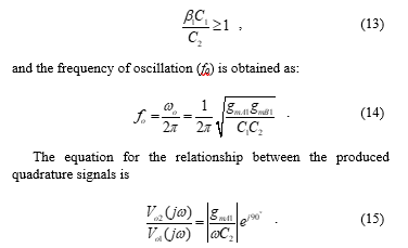
Supply voltages
(V) |
Technology |
| [2] | 2005 | CCII+ = 2 | R = 2, C = 2 | no | yes | no | NA | 15.9 k | ±12 (experiment) | AD844 |
| [3] | 2006 | DDCC = 1 | R = 1, C = 1 | no | no | no | NA | 265.4 k | ±3.3 (simulate) | 1.2 mm |
| [4] | 2017 | MMCC = 1,
CFA = 1 |
R = 1, C = 1 | yes | no | yes | NA | 9.91 M | NA | AD835,
AD844 |
| [5] | 2000 | CDBA = 1 | R = 1, C = 1 | no | no | no | NA | 1.59 M | ±2.5 (simulate) | 0.8 mm |
| [6] | 2001 | CCCII+ = 1 | R = 1, C = 1 | yes | no | yes | NA | 10 M | ±2.5 (simulate) | 0.35 mm |
| [7] | 2015 | VDGA = 1 | R = 1, C = 1 | yes | yes | yes | 1.45 m | 429 k | ±1.5 (simulate) | 0.35 mm |
| [8] | 2017 | VDBA = 1 | R = 1, C = 1 | yes | no | yes | 0.37 m | 1.06 M | ±0.75 (simulate) | 0.25 mm |
| [9] | 2019 | LT1228 = 1 | R = 2, C = 1 | yes | no | yes | NA | 100 k | ±5
(simulate) |
LT1228 |
| [10] | 2010 | FDCCII = 1 | R = 2, C = 1 | no | no | no | NA | 1.59 M | ±3.3 (simulate) | 0.35 mm |
| [11] | 2012 | DDCC = 2 | R = 1, C = 1 | no | no | no | NA | 15.91 M | ±2.5 (simulate) | 0.5 mm |
| [12] | 2011 | FDCCII = 1 | R = 1, C = 1 | no | no | no | NA | 2.65 M | ±1.3 (simulate) | 0.35 mm |
| [13] | 2012 | DDCC = 2 | R = 1, C = 1 | no | no | no | NA | 1.17 M | ±2.5 (simulate) | 0.5 mm |
| [14] | 2019 | Fig.2: CFOA = 2
Fig.3: CFOA = 3 |
Fig.2: R = 5, C = 1
Fig.3: R = 6, C = 1 |
no | yes | no | Fig.2: 0.26,
Fig.3: 0.39 |
7.59 k | ±10 (experiment) | AD844 |
| [15] | 2020 | VCII+ = 2 | R = 3, C = 1 | no | yes
(TM) |
no | 1.22 m | 636.6 k | ±0.9 (simulate) | 0.18 mm |
| [16] | 2020 | EXCCII = 1 | R = 2, C = 2 | no | no | no | 0.7 m | 3.18 M | ±1.2 (simulate) | 0.25 mm |
| [17] | 2021 | ICCII+ = 2 | Fig.2: R = 1 , C = 1
Fig.3: C = 1 |
Fig.2: no,
Fig.3: yes (active resistor) |
no | Fig.2: no,
Fig.3: yes |
3.29 m (simulate) | 7.96 M (simulate),
159 k (experiment) |
±0.75 (simulate),
±9 (experiment) |
0.13 mm,
AD844 |
| [18] | 2021 | CFOA = 2 | Fig.1: R = 3, C = 1
Fig.2: R = 4, C = 1 |
no | yes | no | NA | 33.829 k | ±8 (simulate/ experiment) | AD844 |
| [19] | 2021 | FDCCII = 1 | C = 1 | yes
(active resistor) |
no | yes | 2 m | 6.37 M | ±1.25
(simulate) |
0.25 mm |
| [20] | 2022 | DVCC = 2 | Fig.1 : R = 1, C = 1
Fig.2 : R = 3, C = 1 |
no | Fig.1: no
Fig.2: yes |
no | 0.6 | 62.41 k | ±5 (simulate) | AD844 |
| This work | 2022 | VDGA = 1 | C = 1 | yes | yes | yes | 1.56 m (simulate) | 1.59 M (simulate),
159 k (experiment) |
±0.75 (simulate),
±5 (experiment) |
0.25 mm,
LM13600 |
Abbreviation:
NA = Not Available
CCII = second-generation current conveyor, DDCC = differential difference current conveyor,
MMCC = Multiplication Mode Current Conveyor, CFA = current feedback operational amplifier,
CDBA = current differencing buffered amplifier, CCCII+ = plus-type current-controlled current conveyor,
VDBA = voltage differencing buffered amplifier, FDCCII = fully differential current conveyor,
CFOA = current feedback operational amplifier, VCII+ = plus-type second-generation voltage conveyor,
EXCCII = extra-X second generation current conveyor, ICCII+ = plus-type second-generation current conveyor,
DVCC = differential voltage current conveyor, TM = transimpedance-mode
2. Proposed Circuit Configuration
The VDGA was first introduced in [21], as illustrated in Figure 1. The VDGA device is a six-port versatile active building block described by the following matrix equation [21]-[22]:
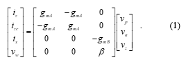
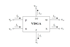
Figure 1: Circuit symbol of the VDGA.
In (1), gmk (k = A, B, C) and β represent the transconductance gain and the voltage transfer gain of the VDGA, respectively. This element has two high input impedance voltages (vp and vn), three high output impedance currents (iz, izc and ix), and a zero output impedance voltage (vw).
The values of gmk and b, when implemented in CMOS technology such as that depicted in Figure 2 [22]-[23], can be expressed as follows:

where K = m0Cox is the transistor transconductance, m0 is the carrier mobility, Cox is the gate-oxide capacitance per unit area, and W/L is the width-to-length ratio of the transistor. From Figure 2, the CMOS VDGA is made up of three sections of transconductance amplifiers (M1A – M9A, M1B – M9B and M1C – M9C). Each transconductor contributes its own transconductance gain gmk that is electronically controllable. Consequently, external bias currents IBk can be used to adjust the parameters gmk and b of the VDGA.
Figure 3 depicts the realization of the phase shifter circuit that requires only one VDGA and one floating capacitor without an external resistor requirement. Despite the fact that the capacitor C employed in this realization is floating, a second poly-layer technique is provided by advanced integrated circuit (IC) technology, making it simple to implement [24]. A preliminary analysis of the proposed configuration in Figure 3 gives the voltage transfer function shown below
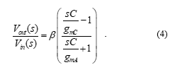
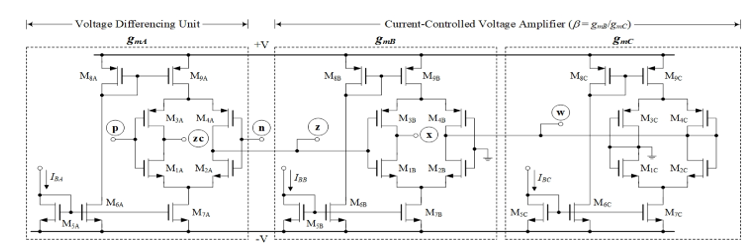
Figure 2: CMOS internal structure of the VDGA.
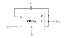
Figure 3: Proposed single VDGA-based resisotrless phase shifter circuit.
Assuming gm = gmA = gmC, the passband gain (H0), pole frequency (fp) and phase response (f) of the configuration are obtained as:
Thus, the transconductances gmk or by changing the external bias currents IBk can be modified to alter the values of H0, ωp and f. Also noticed is the fact that the gain b can be controlled to provide orthogonal H0 control.
3. Effects of Non-Ideal Gains
Ideally, the VDGA features are thought to be perfect. However, due to device mismatch, transfer errors may occur in CMOS implementations of VDGA, deviating from the expected behavior. The impact of the VDGA non-idealities on the functioning of the suggested circuit must thus be investigated. In view of VDGA’s non-ideal gains, (1) may be changed and expressed as:
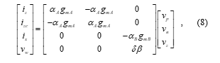
where ak = 1 – ea represents the transconductance inaccuracy coefficient, and d = 1 – ed represents the parasitic voltage transfer gain. Here, ea (|ea| << 1) and ed (|ed| << 1) are the undesirable parameters deviating from unity due to the transfer errors of the VDGA. For the non-ideal analysis of the suggested phase shifter circuit in Figure 3, the modified parameters H0, fp, and f can be given by the following expressions:
It is evident from (9)-(11) that the circuit parameters H0, fp and f are slightly affected by the unwanted factors ak and d of the VDGA. However, this effect can be diminished by modifying the transconductance gain gmk for the circuit shown in Figure 3. According to (2), the value of gmk can be modified conveniently by altering the external bias current IBk.
4. Simulation Verification
In order to evaluate the performance of the proposed phase shifter circuit in Figure 3, the CMOS-based VDGA in Figure 2 was simulated with the TSMC 0.25-mm transistor model in PSPICE computer simulation program. Symmetrical supply voltages of +V = -V= 0.75V were used to bias the VDGA. The transistor sizes (W and L) used in the VDGA realization are listed in Table 2.
Table 2: Transistor sizes used in VDGA realization of Figure 2.
| Transistor | W (mm) | L (mm) |
| M1k-M2k | 15 | 0.25 |
| M3k-M4k | 23 | 0.25 |
| M5k-M7k | 4.5 | 0.25 |
| M8k-M9k | 5.5 | 0.25 |
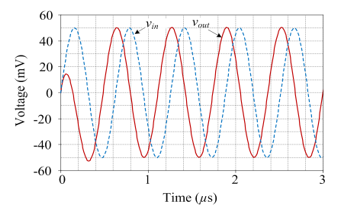
Figure 4: Simulation results of the transient waveforms of the proposed phase shifter in Figure 3.
The active and passive component values are specified as: gmA = gmB = gmC = 1 mA/V, (IBA = IBB = IBC = 100 mA), and C = 0.1 nF for the proposed resistorless phase shifter with H0 = 1 and fp = 1.59 MHz. Figure 4 shows the simulated transient responses of the proposed circuit for an input signal with a sinusoidal frequency of 1.59 MHz and an amplitude of 50 mV (peak). In contrast to the theoretical value of f = 90°, the simulation results show a phase difference between vin and vout of f = 92°.
Figure 5 also shows the simulation outcomes for the gain and phase frequency characteristics in comparison to the ideal curves. The simulated fp is approximately 1.585 MHz, resulting in a frequency error of 0.31 %. The simulation results clearly show that they closely match the theoretical predictions, demonstrating the usefulness of the suggested circuit. It is discovered that the simulated power dissipation of the circuit is around 0.82 mW, when the input vin is kept grounded.
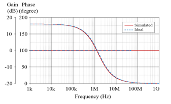
Figure 5: Ideal and simulated frequency characteristics of the proposed phase shifter in Figure 3.
Figure 6 depicts the electronic tuning of H0 without altering the f-value by controlling the gmB-value. The values of the circuit components for these settings are listed in Table 3. The sinusoidal input waveform in these figures is 20 mV (peak) at f = 1.59 MHz. While gmA = gmC = 1 mA/V (IBA = IBC = 100 mA) remains constant, the values of gmB are altered between 0.707 mA/V, 1 mA/V, and 1.414 mA/V (IBB = 50 mA, 100 mA, and 200 mA). These facts lead to the b-value being, respectively, 0.707, 1, and 1.414.
Table 3: Component values for electronic tuning of H0 with IBB.
| IBB
(mA) |
gmB
(mA/V) |
IBA = IBC
(mA) |
gmA = gmC
(mA/V) |
b
(gmB/gmC) |
| 50 | 0.707 | 100 | 1 | 0.707 |
| 100 | 1.000 | 100 | 1 | 1.000 |
| 200 | 1.414 | 100 | 1 | 1.414 |
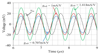
Figure 6: Simulated transient waveforms of the proposed phase shifter with tuning gmB value.
The simulated transient responses of the circuit and its corresponding phase response are also shown in Figures 7 and 8 for three different values of gm, i.e., gm = gmk = 0.707 mA/V, 1 mA/V and 1.414 mA/V (IBk = 50 mA, 100 mA, and 200 mA). The computed values of f were determined to be, respectively, 70.5°, 90°, and 109.4°. The measured f values based on the simulation results were 73°, 92.1°, and 110.2°, respectively, which accord quite well with the estimated values.
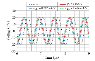
Figure 7: Simulated transient waveforms of the proposed phase shifter with tuning gmk value.
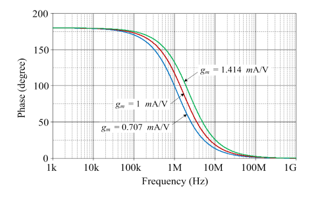
Figure 8: Simulated frequency characteristics of the proposed phase shifter with tuning gm value.
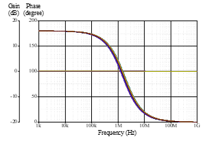
Figure 9: Monte Carlo statistical analysis for the frequency responses of the proposed phase shifter circuit with 5% capacitor tolerance.
In order to demonstrate the impact of capacitor tolerance on the gain and phase responses, a Monte Carlo analysis with a hundred runs is performed for the proposed phase shifter circuit given in Figure 3. It is supposed that the value of capacitor C will change uniformly by 5%. Figure 9 depicts the simulated frequency responses of Monte Carlo statistical analysis. In addition, the results of the Monte Carlo analysis indicate that the mean and sigma of fp are approximately 1.589 MHz and 2.204 ´ 1010, respectively. It can be clearly seen from Figure 9 that the capacitance tolerance has a minor effect on the frequency response of the proposed circuit.
5. Experimental Measurements
Experimental measurement was used to validate the practicability of the designed circuit in Figure 3. The schematic for the practical implementation of the VDGA is shown in Figure 10 [25], using readily available IC dual-OTA LM13600s from National Semiconductor [26]. For LM13600s, the DC bias voltages are +V= -V= 5V.
The proposed phase shifter circuit of Figure 3 was constructed with the following component values: gmk = 1 mA/V (IBk = 100 mA) and C = 1 nF. For time-domain analysis, the circuit was applied with a sinusoidal input of frequency 159 kHz and of amplitude 50 mV (peak). The measured waveforms for vin and vout are shown in Figure 11. The measured f is 92.8°, which is close to the theoretical f of 90°. Accordingly, the measured phase error is about 3.11%. Figure 12 also shows the measured Fourier spectrum of the output waveform vout at 159 kHz.
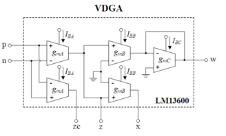
Figure 10: Practical realization of VDGA using readily available IC LM13600s
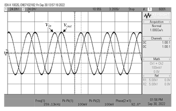
Figure 11: Measured time-domain waveforms of vin and iin for the propose circuit in Figure 3.
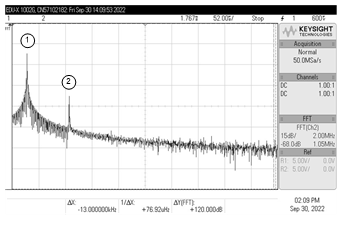
Figure 12: Measured spectrum frequency of vout at 159 kHz (No.1: Frequency = 159 kHz, Gain = -28.91 dB, and No.2: Frequency = 479 kHz, Gain = -29.13 dB)
The next observation on the circuit is carried out on its frequency response characteristic. The measured frequency responses in comparison to the theoretical responses are given in Figure 13. The measured value of fp is found to be 158 kHz, which corresponds to the frequency deviation of 0.63%. The experimental testing results show that while the gain response is essentially constant up to the working frequency of roughly 4 MHz, the phase characteristic is found to change with frequency, as predicted. The difference between measured and ideal curves in the high-frequency region is predominantly attributable to the gain-bandwidth product of the IC OTA LM13600s used to implement the circuit [26]. Obviously, higher-speed active devices could produce superior frequency responses.
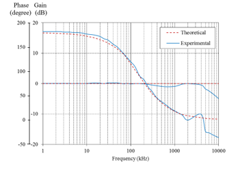
Figure 13: Theoretical and measured frequency responses of the propose circuit in Figure 3.
6. Quadrature Oscillator Application
The quadrature oscillator (QO) circuit can be simply implemented by utilizing the proposed phase shifter circuit, as shown in Figure 14. In the configuration, VDGA2 and C2 create a simple lossless integrator. The following relationship describes the characteristic equation of the QO circuit:
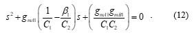
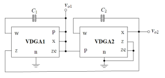
Figure 14: Quadrature oscillator implemented with the proposed circuits.
From the characteristic equation in (12), the condition for oscillation (CO) is satisfied at
Obviously, both quadrature voltages vo1 and vo2 are ideally shifted by a phase (f) of 90°. It may also be observed that gmA1 and C2 have a direct impact on the amplitude ratio of the quadrature voltages. Therefore, it follows that the output voltage amplitude of the QO can be controlled by the values of gmA1 and C2. When the frequency is altered, equal voltage amplitudes can be achieved by changing gmA1 while maintaining C2.
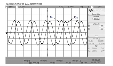
Figure 15: Measured waveforms of the developed QO circuit at vo1 and vo2 outputs.
The following values were chosen for the circuit elements in order to test the functionality of the QO circuit in Figure 14. The selection of gmk = 1 mA/V (IBk = 100 mA) and C1 = C2 = 1 nF for all transconductances and capacitances results in fo = 159 kHz. Figure 15 shows the typical waveforms measured at vo1 and vo2 output terminals with fo = 159.08 kHz and f = 95°. The resulting deviations for fo and f are 0.05% and 5.55%, respectively. The differences from ideal values are mainly attributed to the non-ideal gains and parasitic elements of IC LM13600s, which are described in Section 3. In Figure 16, the corresponding Lissajous figure of the QO circuit is also shown. Figure 17 illustrates the measured spectrum frequency of vo2 of the QO circuit, with the corresponding frequencies and gains at various spectra listed in Table 4. All the results support the practical usefulness of the proposed phase shifter circuit in implementing the quadrature oscillator.
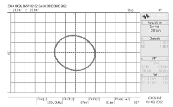
Figure 16: Lissajous figure of the developed QO circuit in Figure 14.
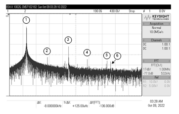
Figure 17: Measured spectrum frequency of vo2 at 159 kHz.
Table 4: Frequencies and gains at different spectrums of Figure 17.
| No. | Frequency (kHz) | Gain (dB) |
| 1 | 159 | -30.798 |
| 2 | 318 | -79.650 |
| 3 | 478 | -63.720 |
| 4 | 620 | -86.022 |
| 5 | 770 | -88.677 |
| 6 | 796 | -89.208 |
7. Conclusions
The paper describes the design of the compact resistorless tunable phase shifter circuit. The described phase shifter circuit requires only one VDGA as an active component and one floating capacitor, resulting in a resistorless architecture and ease of integration. Electronic tuning of the important features of the resulting design, such as the passband gain (H0), pole frequency (fp) and phase response (f), is possible by modifying the gm-values of the VDGA. The non-ideal analysis of the VDGA was also carried out. The voltage-mode quadrature oscillator has been used as an illustrative application for the proposed design. PSPICE simulation data with TSMC 0.25-mm CMOS model parameters have been performed to support the theoretical research. In addition to validating the practical circuit behaviors, experimental measurements with commercially available IC LM13600s have been included.
Conflict of Interest
The authors declare no conflict of interest.
Acknowledgments
This work was supported by King Mongkut’s Institute of Technology Ladkrabang [2566-02-01-041]. The Institute of Research and Development Rajamangala University of Technology Isan, and the Faculty of Engineering, Rajamangala University of Technology Isan, Khonkaen Campus, are also acknowledged for their providing support.
- W. Tangsrirat, T. Pukkalanun and W. Surakampontorn, “Resistorless realization of current-mode first-order allpass filter using current differencing transconductance amplifiers”, Microelectronics Journal, 41(2-3), 178-183, 2010, doi.org/10.1016/j.mejo.2010.02.001.
- J. W. Horng, “Current conveyors based allpass filters and quadrature oscillators employing grounded capacitors and resistors,” Computers & Electrical Engineering, 31(1), 81-92, 2005, doi.org/10.1016/j.compeleceng.2004.11.006.
- J. W. Horng, C. L. Hou, C. M. Chang, Y. T. Lin, I. C. Shiu, and W. Y. Chiu, “First-order allpass filter and sinusoidal oscillators using DDCCs,” International Journal of Electronics, 93(7), 457-466, 2006, doi.org/10.1080/00207210600711481.
- K. Mathur, P. Venkateswaran, and R. Nandi, “All-pass filter based linear voltage controlled quadrature oscillator,” Active and Passive Electronic Components, 2017(4), 1-8, 2017, doi:10.1155/2017/3454165.
- A. Toker, E. O. Gune, and S. Ozoguz, “Current-mode all-pass filters using current differencing buffered amplifier and a new high-Q bandpass filter configuration,” IEEE Transactions on Circuits and Systems-II: Analog and Digital Signal Processing, 47(9), 949-954, 2000, doi.org/10.1109/82.868465
- A. Toker, E.O. Gune, and S. Ozoguz, “New high-Q band-pass filter configuration using current controlled current conveyor based all-pass filters,” in the 8th International Conference on Electronics, Circuits and Systems (ICECS 2001), 165-168, 2001.
- J. Satansup, and W. Tangsrirat, “Single VDGA-based first-order allpass filter with electronically controllable passband gain,” in the 7th International Conference on Information Technology and Electrical Engineering (ICITEE 2015), 106-109, 2015.
- O. Channumsin, and W. Tangsrirat, “Single VDBA-based phase shifter with low output impedance,” in the 14th International Conference on Electrical Engineering/Electronics, Computer, Telecommunications and Information Technology (ECTI-CON 2017), 427-430, 2017.
- A. Chaichana, S. Siripongdee, and W. Jaikla, “Electronically adjustable voltage-mode first-order allpass filter using single commercially available IC,” in International Conference on Smart Materials Applications, Tokyo, Japan, 559(1), 012009, 2019.
- S. Maheshwari, J. Mohan, and D. S. Chauhan, “Voltage-mode cascadable all-pass sections with two grounded passive components and one active element,” IET Circuits, Devices and Systems, 4(2), 113-122, 2010, doi.org/10.1049/iet-cds.2009.0167.
- D. S. Chauhan, G. Garg, J. Mohan, and S. Maheshwari, “Two DDCC based cascadable voltage-mode first-order all-pass filters,” in International Conference on Advances in Electronics, Electrical and Computer Science (EEC 2012), 290-294, 2012.
- B. Metin, N. Herencsar, and K. Pal, “Supplementary first-order all-pass filters with two grounded passive elements using FDCCII,” Radioengineering, 20(2), 433-437, 2011.
- B. Chaturvedi, and S. Maheshwari, “An ideal voltage-mode all-pass filter and its application,” Journal of Communication and Computer, 9, 613-623, 2012.
- E. Yuce, R. Verma, N. Pandey, and S. Minaei, “New CFOA-based first-order all-pass filters and their applications,” International Journal of Electronics and Communications (AEU), 103, 57-63, 2019, doi.org/10.1016/j.aeue.2019.02.017.
- E. Yuce, L. Safari, S. Minaei, G. Ferri, and V. Stornelli, “New mixed-mode second-generation voltage conveyor based first-order all-pass filter,” IET Circuits, Devices & Systems, 14(6), 901-907, 2020, doi.org/10.1049/iet-cds.2019.0469.
- J. Jitender, J. Mohan, and B. Chaturvedi, “A novel voltage-mode configuration for first order all-pass filter with one active element and all grounded passive components,” in the 6th International Conference on Signal Processing and Communication (ICSC 2020), 2020.
- E. Yuce, and S. Minaei, “A new first-order universal filter consisting of two ICCII+s and a grounded capacitor,” International Journal of Electronics and Communications (AEU), 137, 153802, 2021, doi.org/10.1016/j.aeue.2021.153802.
- R. Senani, D. R. Bhaskar, and P. Kumar, “Two-CFOA-grounded-capacitor first-order all-pass filter configurations with ideally infinite input impedance,” International Journal of Electronics and Communications (AEU), 137, 153742, 2021, doi.org/10.1016/j.aeue.2021.153742.
- J. Jitender, J. Mohan, and B. Chaturvedi, “CMOS realizable and highly cascadable structures of first-order all-pass filters,” Walailak Journal of Science and Technology (WJST), 18(14), 21451, 2021, doi.org/10.48048/wjst.2021.21451.
- A. Raj, D. R. Bhaskar, R. Senani, P. Kumar, “Four unity/variable gain first-order cascaded voltage-mode all-pass filters and their fully uncoupled quadrature sinusoidal oscillator applications,” Sensors, 22(16), 6250, 2022, doi.org/10.3390/s22166250.
- J. Satansup, W. Tangsrirat, “CMOS realization of voltage differencing gain amplifier (VDGA) and its application to biquad filter,” Indian Journal of Engineering and Material Sciences, 20(6), 457-464, 2013.
- O. Channumsin, T. Pukkalanun and W. Tangsrirat, “Single VDGA-based dual-mode multifunction biquadratic filter and quadrature sinusoidal oscillator,” Informacije MIDEM-Journal of Microelectronics, Electronic Components and Materials, 50(2), 125-136, 2020, doi.org/10.33180/InfMIDEM2020.205.
- W. Tangsrirat, T. Pukkalanun, O. Channumsin, “Dual-mode multifunction filter realized with single voltage differencing gain amplifier (VDGA)”, Engineering Review, 41(2), 1-14, 2021, doi.org/10.30765/er.1441
- R. J. Baker, H. W. Li, and D. E. Boyce, CMOS circuit design, layout and simulation, Chapter 7, IEEE Press, New York, 1998.
- N. Roongmuanpha, W. Tangsrirat, T. Pukkalanun, “Single VDGA-based mixed-bode universal filter and dual-mode quadrature oscillator”, Sensors, 22(14), 5303, 2022, doi.org/10.3390/s22145303.
- National Semiconductor. Dual operational transconductance amplifiers with linearizing diodes and buffers. LM13600 datasheet 1998.