
Active Simulation of Grounded Parallel-Type Immittance Functions Employing VDBAs and All Grounded Passive Components
Volume 8, Issue 1, Page No 131-137, 2023
Author’s Name: Pratya Mongkolwai1, Pitchayanin Moonmuang2, Worapong Tangsrirat2,a), Taweepol Suesut2
View Affiliations
1Department of Instrumentation Engineering, Faculty of Engineering, Rajamangala University of Technology Rattanakosin, Nakhon Pathom 73170, Thailand
2Department of Instrumentation and Control Engineering, School of Engineering, King Mongkut’s Institute of Technology Ladkrabang, Bangkok 10520, Thailand
a)whom correspondence should be addressed. E-mail: worapong.ta@kmitl.ac.th
Adv. Sci. Technol. Eng. Syst. J. 8(1), 131-137 (2023); ![]() DOI: 10.25046/aj080116
DOI: 10.25046/aj080116
Keywords: Voltage Differencing Buffered Amplifier (VDBA), Immittance function, Impedance simulator

Export Citations
This communication proposes a grounded immittance function simulator that, depending on the proper choice of the passive components, can simulate parallel-type impedances of the R-L, R-C, and L-C forms. Only two grounded passive components and two voltage differencing buffered amplifiers (VDBAs) are used to implement the suggested circuit. All three simulated equivalent elements, namely Req, Leq, and Ceq, can be electronically adjusted through the VDBA’s transconductance gain. The impact of the non-ideality of the VDBA device on the developed simulator is examined in detail. The voltage-mode bandpass filter has been implemented using the suggested active LC parallel impedance simulator to show that it performs as predicted. To prove the theory, the proposed circuit is simulated using the PSPICE tool. The findings of the experimental measures are also presented to demonstrate the circuit’s feasibility.
Received: 08 October 2022, Accepted: 15 January 2023, Published Online: 24 February 2023
1. Introduction
Electronic devices have assimilated into our daily lives in the world today. The development of novel technologies will be influenced by the published findings. In several analog signal processing solutions, the different active devices, such as current conveyor (CC), operational transconductance amplifier (OTA), current feedback operational amplifier (CFOA), and current differencing buffered amplifier (CDBA), have gained widespread attention. Similarly, since 2008, the voltage differencing buffered amplifier (VDBA) has been recognized as one of the most versatile and practical devices [1]-[2].
The VDBA element has a tunable transconductor as the input section and a voltage buffer as the output section. Because of this feature, this active element can be used in a variety of voltage-mode, current-mode, and mixed-mode analog circuits and applications [2–6]. Passive elements, such as resistors, capacitors, and inductors, were used in a variety of applications, including analog active filter circuits, sinusoidal oscillator design, and impedance cancellation circuit. However, when applied in the implementation of an integrated circuit (IC), the behavior of passive elements was constrained by its enormous size and suffered from electronic tuning properties. As a consequence, an IC that mimicked the behavior of a passive element was implemented using an active element [7-9]. The parallel-type R-L simulators that were suggested in the literature [10–12] needed at least three active components. Similar to that, three or more passive components are required to realize the circuits in [11–12]. The circuits in [13] also need a high-voltage operation.
Therefore, the contribution of this work is to propose a grounded parallel R-L, R-C, and L-C impedance simulator, which depends on the appropriate selection of the passive element being used. The suggested simulator circuit uses only two VDBAs, two grounded passive components, and allows electronically control of the equivalent simulated elements via the transconductance gains of the VDBAs. In this study, the VDBA non-ideality effect on the actual immittance simulator is examined. With 0.18-mm CMOS technology, the proposed R-L, R-C, and L-C impedance simulator circuit in frequency domain was simulated using PSPICE program. Time-domain analysis and temperature-dependent simulation are also carried out in the parallel R-C simulator. The theoretical analysis is validated by experimental laboratory measurements using commercially available IC LT1228. Additionally, the active L-C simulator has also been used to apply a second-order voltage-mode bandpass filter in order to validate the viability. All results, both from simulations and experiments, are discovered to be in accordance with the theoretical predictions.
2. Fundamental of VDBA
Figure 1 depicts the electrical symbol of the VDBA element. This functional block has two input terminals (p and n) that meet high input impedance criteria and two output terminals (z and w), which have high and low impedances, respectively. Under ideal operating condition, the effective transconductance gain (gm) of the VDBA converts the differential voltage between vp and vn (vp – vn) into an output current (iz) at terminal z. The voltage drop (vz) at the z terminal is transferred to the output voltage (vw) at the w terminal. From its ideal operating condition, the following matrix equation can be used to characterize the terminal relationship of the VDBA [1-2]:
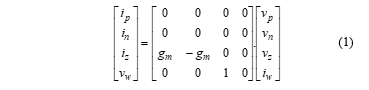
In general, the gm value in (1) can be changed by electronic means via the external bias voltage or current.
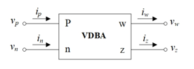
Figure 1: Schematic symbol of the VDBA.
In non-ideal assumption, the characteristic of VDBA can be modified as [3]:
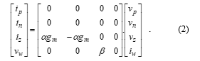
In above expression, a = (1 – egm) and b = (1 – ev), where |egm | << 1 and and |ev | << 1 stand for transconductance inaccuracy coefficient and the voltage tracking error, respectively.
A CMOS model of VDBA consisting of the differential amplifiers with active load (M1-M4 and M7-M10), and the source follower (M11) is shown in Figure 2. For the CMOS VDBA in Figure 2, the relationship between gm and the bias current IB can be characterized as follows [4]:
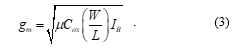
Here, m is the effective carrier mobility, Cox is the gate-oxide capacitance per unit area, and W and L are the effective channel width and length of M1 and M2 transistors, respectively.
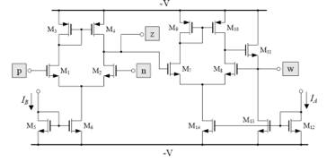
Figure 2: CMOS model of the VDBA used in this work.
3. Proposed Parallel-Type Immittance Function Simulator
According to Figure 3, the suggested grounded parallel-type immittance simulator is made up of two VDBAs and two grounded passive components. Based on ideal condition consumption, the input admittance (Yin) of the circuit is derived as:
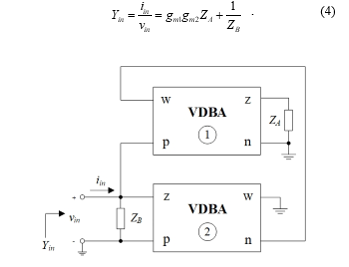
Figure 3: Proposed grounded parallel-type immittance function simulator.
The proposed parallel R-L, R-C, and L-C immittance simulator was made achievable by selecting the appropriate passive components, which describes the realized circuit. Its simulated impedances are summarized in Table 1, which illustrates that all synthetic simulator values can electronically be changed by the transconductance gmi of the i-th VDBA (i = 1, 2). Since all of the passive components are grounded, the configuration is attractive from further integration point of view. Another attractive feature of the design is that it does not need any special component equality for its realization.
Under the non-ideal operation given in (2), the results of reevaluating the proposed circuit in Figure 3 can be summarized in Table 2.
Table 1: Equivalent Circuit and Corresponding Equivalent Values for Figure 3 in Ideal Case
| ZA | ZB |
Equivalent circuit |
Equivalent values |
| 1/sCA | RB | parallel R-L | , |
| RA | 1/sCB | parallel R-C | , |
| 1/sCA | 1/sCB | parallel L-C | , |
Table 2: Equivalent Element Values for Figure 3 in Non-Ideal Case
| ZA | ZB |
Equivalent circuit |
Equivalent values |
| 1/sCA | RB | parallel R-L | , |
| RA | 1/sCB | parallel R-C | , |
| 1/sCA | 1/sCB | parallel L-C | , |
The sensitivity coefficients of the simulated equivalent values, Req Leq and Ceq, are each affected by the active and passive circuit components, and the finding values are produced as follows.
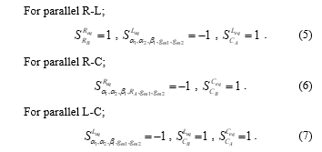
All of the sensitivity coefficients from above (5) to (7) have magnitudes that are less than or equal to one. As a result, the sensitivity of all the proposed parallel R-L, R-C, and L-C immittance simulators is quite low.
4. Simulation Results
PSPICE simulation program has been used to simulate the suggested grounded parallel-type impedance simulator in Figure 3. The simulator was designed employing CMOS VDBA of Figure 2 with a model of 0.18-mm process parameters from TSMC. Table 3 lists the computed aspect ratio (W/L) for each transistor. The supply voltages used to bias this circuit were +V= -V= 0.75 V.
Table 3: Calculated transistor dimensions of VDBA in Figure 2
| Transistor | W/L (mm/mm) |
| M1-M2, M5, M7-M8, M12-M13 | 2.4/0.18 |
| M3, M9, M14 | 5/0.18 |
| M4, M10 | 5.2/0.18 |
| M6 | 3.25/0.18 |
| M11 | 10/0.18 |
The following components were chosen for simulations: IB1 = IB2 = 90 mA for gm = gm1 = gm2 = 0.641 mA/V, RA = RB = 1 kW, and CA = CB = 50 pF. Using data from Table 1, the simulated equivalent values of Figure 3 can be derived as:
- for R-L simulator: Req = 1 kW and Leq = 0.12 mH;
- for R-C simulator: Req = 2.44 kW and Ceq = 50 pF;
- for L-C simulator: Leq = 0.12 mH and Ceq = 50 pF.
The total power consumed in the circuit for this setting was found to be 0.388 mW.
Based on the results of the simulation and theory, Figure 4 depicts the magnitude and phase frequency characteristics of the proposed parallel-type immittance simulator circuit in Figure 3. The frequency corners (fc) of the R-L and R-C impedance simulators in Figs. 4(a) and 4(b) obtained from the simulation results are found to be roughly 1.29 MHz, which is pretty close to the calculated value of 1.30 MHz. In addition, the simulated fc value of the L-C impedance simulator was discovered to be 2.04 MHz, which nearly equals to the ideal value of fc = 2.05 MHz. The input voltage (vin) and current (iin) responses through the R-C impedance simulator are also displayed in Figure 5 as simulated time-domain waveforms. This performance was evaluated by supplying a sinusoidal input signal with a peak value of 50 mV at f = 1 MHz to the simulated RC impedance circuit.
In order to further illustrate the electronic adjustability of the proposed circuit, the parallel L-C simulator has been performed to change IB = IB1 = IB2 = 50 mA, 100 mA, and 200 mA, while maintaining CA = CB = 50 pF. As a consequence, the simulated equivalent inductance value (Leq) has been altered to 0.22 mH, 0.11 mH, and 54.8 mH, respectively, while the simulated equivalent capacitance value (Ceq) remains constant at 50 pF. The results of the simulated frequency responses compared with the theory are given in Figure 6.
The impact of varying ambient temperature variation on the simulator responses is also being considered. This was accomplished by testing the proposed R-C simulator circuit with changes in ambient temperature ranging from 0°C to 100°C with steps of 25°C. Figure 7 displays the result of its magnitude variations.
5. Experimental Results
In order to further confirm the feasibility of the proposed idea, the suggested circuit of Figure 3 has been tested in the laboratory utilizing IC LT1228 from Linear Technology [14]. The package information and internal behavior of IC LT1228 are shown in Figure 8. There are two amplifiers: OTA and CFOA. The OTA is used to provide a high-impedance differential input and a current source output with wide output voltage compliance, while the CFOA is utilized to transmit voltage from the z terminal to the o terminal, and the current from the z terminal to the x terminal. According to the following relation, the transconductance gain (gm) of the LT1228 in this case is reliant on the external bias current (IB) [14]:
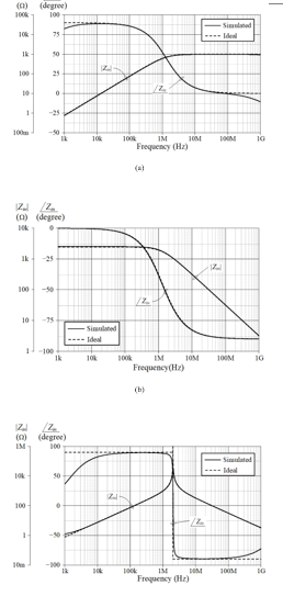
Figure 4: Ideal and simulated frequency responses of the proposed parallel-type immittance simulator circuit in Figure 3. (a) R-L impedance simulator (b) R-C impedance simulator (c) L-C impedance simulator
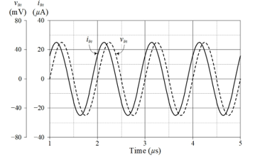
Figure 5: Simulated time-domain responses for vin and iin of the R-C simulator.
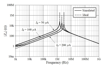
Figure 6: Simulated frequency responses of the L-C simulator with varying IB.
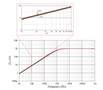
Figure 7: Simulated frequency responses of the R-C simulator at different temperature (0°C, 25°C, 50°C, 75°C, and 100°C).
![]()
In the case of parallel R-L impedance simulation, the active and passive components for the experimental measurement were taken as follows: gm = gm1 = gm2 = 0.5 mA/V (IB = IB1 = IB2 = 50 mA), RB = 1 kΩ, and CA = 1 nF, resulting in Req = 1 kΩ, and Leq = 4 mH. With symmetrical supply voltages of ±5 V, the LT1228 was biased. Figure 9 shows the grounded parallel lossy inductor’s measured magnitude and phase responses for the selected components.
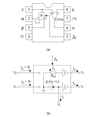
Figure 8: IC LT1228 (a) package information (b) its internal behavior.
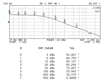
Figure 9: Measured frequency responses of the parallel R-L simulator (a) magnitude response (b) phase response
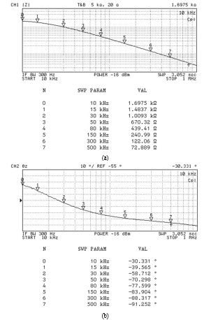
Figure 10: Measured frequency responses of the parallel R-C simulator (a) magnitude response (b) phase response
The parallel R-C simulator was then tested with the following parameters: gm = gm1 = gm2 = 1 mA/V (IB = IB1 = IB2 = 100 mA), RA = 500 Ω, and CB = 4.7 nF, yielding Req = 2 kΩ, and Ceq = 4.7 nF. Figure 10 shows the measured frequency responses for the equivalent input impedance of the simulator. The experimental results shown in Figures 9 and 10 demonstrate the suggested circuit’s practicality in application areas.
6. Application Example
The second-order voltage-mode bandpass filter in Figure 11(a) is intended to emphasize operational performance as an illustration of an application. The bandpass filter realization utilizing the proposed L-C parallel immittance simulator in Figure 3 is shown in Figure 11(b). The voltage transfer action of the filter is written as:
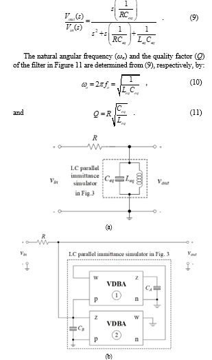
Figure 11: Second-order voltage-mode bandpass filter (a) prototype passive structure (b) utilizing the L-C simulator in Figure 3.
The simulated frequency response of the implemented active bandpass filter is demonstrated in Figure 12 with the following components: R = 1.5 kW, gm = gm1 = gm2 = 0.675 mA/V (IB = IB1 = IB2 = 100 mA), and CA = CB = 100 pF. With Leq = 0.22 mH and Ceq = 100 pF, the filter is designed to obtain fo = wo/2p = 1.07 MHz and Q = 1. The resulting responses demonstrate that the circuit can operate correctly between 500 kHz and 100 MHz.
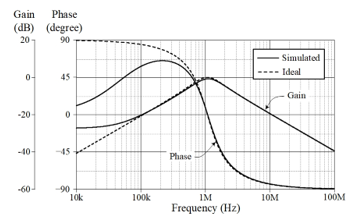
Figure 12: Ideal and simulated results of the bandpass frequency responses in Figure 11(b).
7. Conclusions
A grounded parallel RL, RC, and LC impedance simulator has been designed with VDBAs and two grounded passive components. Through the use of the transconductance parameter in VDBA, the simulated equivalent values, i.e., Req, Leq, and Ceq, can all be electronically altered. The circuit has been simulated using the PSPICE program, which is based on 0.18-mm CMOS technology, to demonstrate its viability. In-depth laboratory tests have also been conducted to verify the practical usability of the simulator circuit. The design of a second-order voltage-mode bandpass filter using the proposed simulator is given.
Conflict of Interest
The authors declare no conflict of interest.
Acknowledgments
This work was supported by Rajamangala University of Technology Rattanakosin (RMUTR). The support by the School of Engineering, King Mongkut’s Institute of Technology Ladkrabang, contact no. 2562-02-01-004, is also gratefully acknowledged.
- D. Biolek, R. Senani, V. Biolkova and Z. Kolka, “Active elements for analog signal processing: classification, review, and new proposals”, Radioengineering, 17(4), 15–32, 2008.
- R. Sotner, J. Jerabek, N. Herencsar, N. “Voltage differencing buffered/inverted amplifiers and their applications for signal generation”, Radioengineering, 22(2), 490-504, 2013.
- W. Tangsrirat, “Actively Floating lossy inductance simulators using voltage differencing buffered amplifiers,” IETE Journal of Research, 65(4), 446–459, 2018, doi.org/10.1080/03772063.2018.1433082
- F. Kaçar, A. Yeşil, A. Noori, “New CMOS realization of voltage differencing buffered amplifier and its biquad filter applications,” Radioengineering, 21(1), 333–339, 2012.
- N. Roongmuanpha, T. Pukkalanun, W. Tangsrirat, “Practical realization of electronically adjustable universal filter using commercially available IC-based VDBA,” Engineering Review, 41(3), 1-14, 2021, doi.org/10.30765/re.1547.
- M. Faseehuddin, N. Herencsar, S. Shireen, W. Tangsrirat, S. H. M. Ali, “Voltage differencing buffered amplifier-based novel truly mixed-Mode biquadratic universal filter with versatile input/output features”, Applied Sciences, 12(3), 2022, doi.org/10.3390/app12031229.
- P. Moonmuang, T. Pukkalanun, W. Tangsrirat, “Floating/grounded series/parallel R-L, R-C and L-C immittance simulators employing VDTAs and only two grounded passive elements,” AEU – International Journal of Electronics and Communications, 145, 154095, 2022, doi.org/10.1016/j.aeue.2021.154095.
- P. Moonmuang, W. Tangsrirat, “Single VDTA-based tunable floating lossy inductance simulation circuits,” IETE Journal of Research, doi: 10.1080/03772063.2021.1900752.
- N. Roongmuanpha, W. Tangsrirat, “Practical floating capacitance multiplier implementation with LT1228s,” Informacije MIDEM- Journal of Microelectronics, Electronic Components and Materials, 51(1), 85-94, 2021, doi.org/10.33180/InfMIDEM2021.106
- A. Paul and D. Patranabis, “Active simulation of grounded inductors using a single current conveyor”, IEEE Transactions on Circuits and Systems, 28(2), 164-165, 1981, doi.org/10.1109/TCS.1981.1084947
- H. Kuntman, M. Gülsoy and O. Çiçekoğlu, “Actively simulated grounded lossy inductors using third generation current conveyors”, Microelectronics Journal, 31(4), 245-250, 2000, doi.org/10.1016/S0026-2692(99)00108-1
- O. Çiçekoğlu, A. Toker and H. Kuntman, “Universal immittance function simulators using current conveyors”, Computers and Electrical Engineering, 27(3), 227-238, 2001, doi.org/10.1016/S0045-7906(00)00018-5
- F. Kaçar and H. Kuntman, “CFOA-based lossless and lossy inductance simulators”, Radioengineering, 20(3), 627-631, 2011.
- Linear Technology, “100MHz current feedback amplifier with DC gain control”, LT1228 datasheet, 1994.