Characterization and Investigating the Effect of Gate-Insulator Thickness on Co-Axial Cylindrical Carbon Nanotube Field Effect Transistor

Adv. Sci. Technol. Eng. Syst. J. 8(1), 12–16 (2023);
 DOI: 10.25046/aj080102
Carbon nanotube field effect transistor (CNTFET) has a huge advantage over the Si- MOSFET. In MOSFET switching occurs by altering channel resistivity whereas in CNTFET switching occurs by modulation contact resistance. CNTFET generates three to four times of drive current than MOSFET. Transconductance of CNTFET is four times higher than the MOSFET. The average carrier velocity is also very high almost double in CNTFET than that is in MOSFET. Its power consumption is low. Electron mobility is high. Threshold voltage is also low. It has better control over channel formation. There is no direct tunneling and gate leakage current is also reduced. Herein, the main objective is to investigate the effect of gate-insulator thickness on CNTFET, and to optimize the thickness so that current carrying capacity may reach higher.A detailed simulations have been made and IV characterizationis done to investigate the effect of Gate-Insulator Thickness on Co-Axial Cylindrical Carbon Nanotube Field Effect Transistor.Report shows with the increasing gate-insulator thickness current is decreased significantly. Where as the variation of nano diameter shows that the increasing rate of current is increased when the carbon tube diameter is increased.
1. Introduction
In this age of nanotechnology, the demand of integrated circuits with smaller dimension has increased. On the other side this fast-moving world requires technology with high speed performance and that can consume lower power. To fulfill such requirements, the use of carbon nanotube field effect transistor (CNTFET) over Si- MOSFET has increased widely. Its ability to carry high current makes it more popular [1]. Carbon nanotubes consist of carbon atoms having diameter in nanometer range [2]. The considerable tiny sized carbon and its electronic configuration ensure unique carbon element with versatile structures and alluring properties [2]. Having the title of the strongest material ever measured, graphene is a two-dimensional (one-atom-thickness) allotrope of carbon with a planar honeycomb lattice [3]. It is regarded as the basic building block of carbon nanotubes. The versatile properties of carbon nanotubes (CNT) basically sourced from graphene [2]. Folding one or multiple graphene sheets with a specific chiral angle creates unique CNT.
Based on the number of folded layers’ carbon nanotubes can be classified in two types.
- Single – walled carbon nanotube (SWNTs), having diameter 1nm [4]
- Multi – walled carbon nanotube (MWNTs), having diameter 100 nm
In multilayer formation many layers are interlinked. On the other hand, another classification of CNTFETs can be mentioned based on its geometry.
In a back-gate CNTFET generally SWCNT is used. It was first proposed by Tans et.al. [5]. The I(on)/ I(off) ratio of this type of CNTFET is almost 105 [6]. The parasitic contact resistance of such CNTFET is very high (>1Mohm) [7]. On the other hand, the drain current as well as the value of transconductance is very low. Drain current is of the nano range [6]. Such limitations of back-gate CNTFET drive the researchers to develop a next generation CNTFET.
Wind et al. have come up with the first top gate CNTFET [8]. In this model the gate is formed over the carbon nanotubes. Though the fabrication process of Top gate CNTFET is little complicated but it is preferred over back-gate CNTFET due to its high drain current of the order of micro and for the greater value of transconductace.
Unlike the other two CNTFETs in Wrap around gate CNTFET the whole nanotube is covered by gate. It is also known as Gate-all-around CNTFET. To expose the ends of the nanotube the wrapping is partially etched and then the source, gate and drain contacts are deposited on the nanotubes. As the entire carbon nanotube is covered, it reduces the leakage current and increases the electrical performance.
In suspended CNTFET method, gate is suspended over a trench to reduce the contact with substrate and gate oxide and it improves the device performance. But the main drawback of such type of CNTFET is here air or vacuum is considered as the dielectric medium. Only short CNTs are used as long tubes may short the device by touching the metal contact.
Depending on the type of electrodes used, the CNTFET classification has been made into three categories. (a) Schottky-barrier (SB) CNTFET (b) Partially gated (PG) CNTFET and (c) doped-S/D CNTFET [9-16]. And the differences are clearly shown in Figure 1.
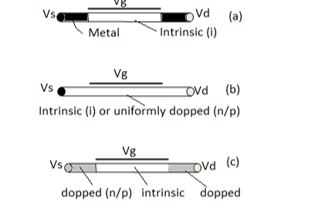
Figure 1: Different types of CNTFET: (a) Schottky-barrier (SB) CNTFET, (b) partially gated (PG) CNTFET (c) doped-S/D CNTFET [9].
Here we have focused on the co-axial cylindrical CNTFET. In such CNTFETs an oxide layer is portrayed arround a cylindrical carbon nano tube. Further a metallic cylindrical layer is deposited in it. This metallic contact can behave as a gate here. At a fixed bias voltage it can induce more channel charge than the other CNTFETs. This is because of its geometry. The capacitive coupling between the gate electrode and the nanotube surface is the maximum for it. Technologies like complementary metal-oxide-semiconductor (CMOS) can be affected by the short channel effects. This improved coupling can prevent this short channel effects. Its geometry of end contact is also important as it can provide the concept of the dimension of Schottky barrier. This Schottky barrier is actually present at the channel near device ends and it can directly influence the current modulation. It also has a huge role in low voltage applications.
2. Simulation of Co-Axial Cylindrical Carbon Nanotube Field Effect Transistor
The In this paper simulations were done for co – axial cylindrical CNTFET using the well-known FETToy tool to see how the characteristic curves depends on different tube parameters like nanotube diameter and gate insulator thickness. Varying the Gate Oxide thickness and nano-tube diameter the drain current can be varied. On the other hand the scaling of the most popular Si-MOSFET almost approaches towards its limiting values. In search of new alternatives this simulation was done to overcome these limitations.
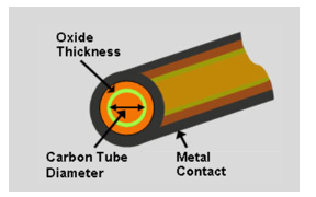
Figure 2: co-axial cylindrical CNTFET
Figure 2 represents a schematic diagram of co-axial cylindrical CNTFET. First for a constant nanotube diameter (1 nm), the simulation was done by varying the gate insulator thickness only. For this simulation the ambient temperature was taken as 300K. Threshold voltage of the used CNTFET was 0.32 V whereas the gate control parameter and drain control parameter were considered as 0.88 and 0.35 respectively. Series resistance was taken zero.
3. Prepare Your Paper before Styling
Before Some data taken during the simulation are given below.
Table 1: (Drain voltage=1 V, Nanotube diameter=1nm)
|
Gate Voltage (V)
|
Drain Current (μA) | ||
| Gate-Insulator thickness
1nm |
Gate-Insulator thickness
1.5nm |
Gate-Insulator thickness
2nm |
|
| 0 | 0.00672 | 0.0000661 | 0.0000661 |
| 0.0833 | 0.114 | 0.00112 | 0.00112 |
| 0.1667 | 1.9 | 0.0187 | 0.0186 |
| 0.2500 | 24.4 | 0.24 | 0.232 |
| 0.3333 | 123 | 1.23 | 1.13 |
| 0.4167 | 296 | 3.01 | 2.69 |
| 0.5000 | 517 | 5.41 | 4.75 |
| 0.5833 | 778 | 8.37 | 7.26 |
| 0.6667 | 1070 | 11.9 | 10.2 |
| 0.7500 | 1400 | 15.9 | 13.7 |
| 0.8333 | 1750 | 20.4 | 17.5 |
| 0.9167 | 2140 | 25.1 | 21.6 |
| 1.0000 | 2550 | 30 | 26 |
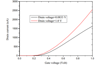
Figure 3: (a) Gate Voltage Vs Drain Current curve for a CNT having diameter 1nm and gate insulator thickness 1nm.
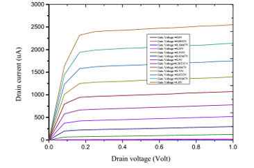
Figure 3: (b) Output Characteristic curve for a CNT having diameter 1nm and gate insulator thickness 1nm .
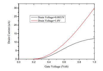
Figure 3: (c) Gate Voltage Vs Drain Current curve for a CNT having diameter 1nm and gate insulator thickness 1.5nm.
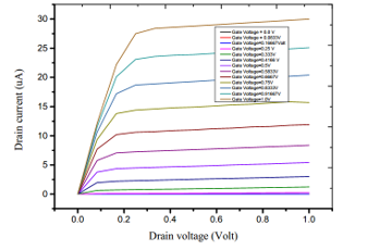
Figure 3: (d) Output Characteristic curve for a CNT having diameter 1nm and gate insulator thickness 1.5nm.
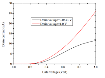
Figure 3: (e) Gate Voltage Vs Drain Current curve for a CNT having diameter 1nm and gate insulator thickness 2nm.
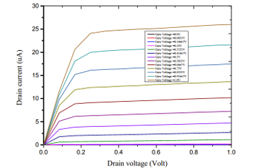
Figure. 3: (f) Output Characteristic curve for a CNT having diameter 1nm and gate insulator thickness 2nm.
From the data of Table-1 it is clear that the drain current vs gate voltage characteristic curve for 1nm gate-insulator thickness is steeper than the other two. Whereas for the same given voltage CNTFET having gate-insulator thickness 2nm gives the lowest drain current. So the drain current is decreased with the increasing gate-insulator thickness. This is due to the fact that with the increase of the gate-insulator thickness the resistance across it is also increased and as a result the drain current is decreased [12]. When the gate dielectric becomes thicker, the electric field within the dielectric becomes smaller for the same gate voltages. Thus the accumulated free carrier near the interface also becomes less. As the carrier density decreases, the drain current decreases as well. Figure 3 shows the input and output characteristic curves for CNTs having different gate insulator thickness but same nanotube diameter i.e. 1nm. Another simulation (shown in figure 4) was done by taking nanotube diameter as 2 nm and varying the gate-insulator thickness from 1nm to 2nm. Other aspects were fixed. I-V characterization is made to investigate the Effect of gate-insulator thickness on co-axial cylindrical CNTFET.
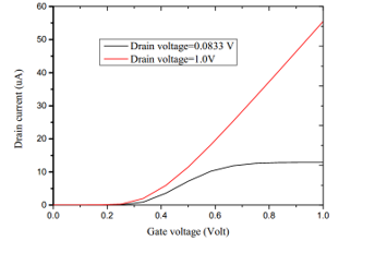
Figure 4: (a) Gate Voltage Vs Drain Current curve for a CNT having diameter 2nm and gate insulator thickness 1nm
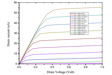
Figure 4: (b) Output Characteristic curve for a CNT having diameter 2nm and gate insulator thickness 1nm
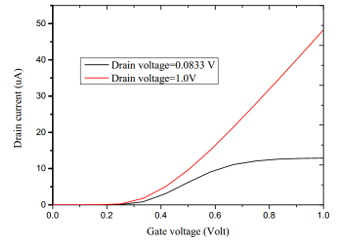
Figure 4: (c) Gate Voltage Vs Drain Current curve for a CNT having diameter 2nm and gate insulator thickness 1.5nm
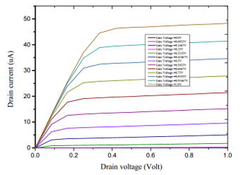
Figure 4: (d) Output Characteristic curve for a CNT having diameter 2nm and gate insulator thickness 1.5nm
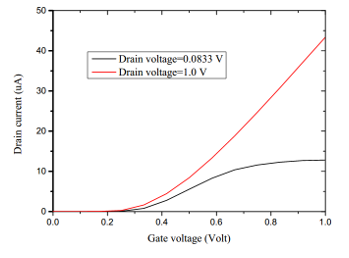
Figure 4: (e) Gate Voltage Vs Drain Current curve for a CNT having diameter 2nm and gate insulator thickness 2nm
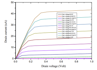
Figure 4: (f) Output Characteristic curve for a CNT having diameter 2nm and gate insulator thickness 2nm
Table 2. (Drain voltage =1 V, Nanotube diameter=2nm) [11]
|
Gate Voltage (V)
|
Drain Current (μA) | ||
| Gate-Insulator thickness
1nm |
Gate-Insulator thickness
1.5nm |
Gate-Insulator thickness
2nm |
|
| 0 | 0.0000661 | 0.0000661 | 0.0000661 |
| 0.0833 | 0.00112 | 0.00112 | 0.00112 |
| 0.1667 | 0.0189 | 0.0189 | 0.0189 |
| 0.2500 | 0.28 | 0.271 | 0.265 |
| 0.3333 | 1.99 | 1.78 | 1.64 |
| 0.4167 | 5.93 | 5.02 | 4.46 |
| 0.5000 | 11.5 | 9.62 | 8.43 |
| 0.5833 | 18.2 | 15.2 | 13.3 |
| 0.6667 | 25.4 | 21.4 | 18.8 |
| 0.7500 | 32.8 | 27.9 | 24.7 |
| 0.8333 | 40.3 | 34.6 | 30.8 |
| 0.9167 | 47.9 | 41.4 | 37.1 |
| 1.0000 | 55.5 | 48.3 | 43.4 |
4. Conclusion
Here we can see that just by changing the nanotube diameter and gate-insulator thickness the drain current can be changed. For the nanotube diameter 1nm and gate-insulator thickness 1nm we get a huge drain current compare to the other combinations. Simulation results ensure the effect of gate dielectric increment in terms of decrement in drain current. It is due to reduction in the electric field for the same gate voltages. Thus the decay in carrier density and drain current.
This CNTFET also has a huge advantage over the Si- MOSFET. In MOSFET switching happens by altering channel resistivity whereas in CNTFET switching is due to modulation contact resistance. CNTFET generates three to four times of drive current than MOSFET. About quadruple higher transconductance of CNTFETs than MOSFETs comes from the band structure and improved mobility. The average carrier velocity is also very high almost double in CNTFET than that is in MOSFET. Its power consumption is low. Electron mobility is high. Threshold voltage is also low. It has better control over channel formation. There is no direct tunnelling and gate leakage current is also reduced.
Conflict of Interest
The authors declare no conflict of interest.
- Raychowdhury, A., & Roy, K. Carbon nanotube electronics: design of high-performance and low-power digital circuits. IEEE Transactions on Circuits and Systems I: Regular Papers, 54(11), 2391-2401, 2007, 10.1109/TCSI.2007.907799
- A. Sarkar, S. Maity, P. Chakraborty , S. K. Chakraborty , “Characterization of carbon nanotubes and its application in biomedical sensor for prostate cancer detection,” American Scientific Publishers, 17, 17-24, 2019, https://doi.org/10.1166/sl.2019.4039
- A. Sarkar, M. Sreenath, K. Srinivas and NV Teja, “Investigation of Graphene as a Sensing Layer for Future Prostate Cancer Biosensing Applications,” Journal of Physics: Conference Series, 1921(1), 2021, 10.1088/1742-6596/1921/1/012038
- T. W. Odom, J. L. Huang et al.,“Atomic structure and electronic properties of single-walled Carbon Nanotubes,” Nature, Nature, 391(6662), 62-64, 1998, https://doi.org/10.1038/34145
- S. J. Tans, A. R. M. Verschueren and C. Dekker, “Room-temperature transistor based on a single carbon nanotube,” Nature , 393(6680), 49-52, 1998, https://doi.org/10.1038/29954
- S. Rasmita and R. R. Mishra, “Simulations of carbon nanotube field effect transistors”, International Journal of Electronic Engineering Research 1(2), 117-125, 2009.
- N. T. Rouf, A. H. Deep and R. B. Hassan, Current-voltage characteristics of carbon nanotube field effect transistor considering non-ballistic conduction, BRAC University Dhaka-1212, Bangladesh.
- S. J. Wind, J. Appenzeller, P. Avouris, “Lateral scaling in carbon nanotube field effect transistors”, P Physical Review Letters, 91(5), 058301, 2003, https://doi.org/10.1103/PhysRevLett.91.05830
- T. Dang, L. Anghel, R. Leveugle, “CNTFET Basics and Simulation. International Conference on Design and Test of Integrated Systems in Nanoscale Technology,” IEEE Explore 2006.
- J. Guo, S. Datta and M. Lundstrom, “Assessment of silicon mos and carbon nanotube fet performance limits using a general theory of ballistic transistors,” IEEE 2015.
- A. Rahman, J. Wang, J. Guo, Md. S. Hasan, Y. Liu, A. Matsudaira, S. S. Ahmed, S. Datta, M. Lundstrom, FETToy, 10254/nanohub-r220.4, 2006.
- M. Radosavljevic, S. Heinze, J. Tersoff, and P. Avouris, “Drain voltage scaling in carbon nanotube transistors”, Applied Physics Letters, 83(12), 2435-2437., 2003, https://doi.org/10.1063/1.1610791
- M. Zhang, P. C. H. Chan, Y. Chai, “Novel Local Silicon-Gate Carbon Nanotube Transistors Combining Silicon-on-Insulator Technology for Integration,” IEEE transactions on nanotechnology, 8(2), 260-268,2009, 10.1109/TNANO.2008.2011773
- Compano, R. ed. “Technology Roadmap for Nanoelectronics,” Microelectronics Advanced Research Initiative, 2000.
- Sagar P., Handa A., Kumar G., Gupta V. Nanocomposite hydrogel materials for defective cartilage repair and its mechanical tribological behavior, A Review. Paper and Biomaterials, 7(3), 63-72, 2022, https://doi.org/10.1213/j.issn.2096-2355.2022.03.007
- Sagar P., Handa A, Kumar G. (2022), Metallurgical, mechanical and tribological behavior of Reinforced magnesium-based composite developed Via Friction stir processing, Proceedings of the Institution of Mechanical Engineers, Part E: Journal of Process Mechanical Engineering, 236(4), 1440-1451, https://doi.org/10.1177/09544089211063099