µPMU Hardware and Software Design Consideration and Implementation for Distribution Grid Applications
 , Mohamed Ahmed Abdellah, Mansour Ahmed Mohamed, Mohamed Abd Elazim Nayel
Adv. Sci. Technol. Eng. Syst. J. 7(4), 59–71 (2022);
 DOI: 10.25046/aj070409
This article presents a roadmap for distribution grid µPMU hardware and software design consideration and implantation to ensure high performance within limited computational time of sampling frequency 512 samples/cycle. A proposed 12 channels, multi-voltage level µPMU hardware and rules of voltage and current transducer, analog filter, analog-to-digital converter, sampling rate definition, and PCB design and selection are presented. From the software view, software minimization procedures are implemented to reduce the estimation time of the proposed µPMU to 18 µsec under high sampling frequency operation. Additionally, error estimation and compensation are used to ensure robust performance, while the computational burden of the error compensation stage is reduced by Taylor series linearization. The proposed µPMU is designed to provide traditional phasor, frequency and harmonics measurements besides a point-on-wave under dynamic operation mode. The proposed device is tested under IEEE Std C37. 118.1 and 118.2 and showed accurate phasor estimation up to 0.03% for the magnitude and angle accuracy up to 0.0036o, while the frequency is estimated with maximum variation of 0.032% under dynamic operation.
1. Introduction
Distribution grids modern structure is more dynamic in nature due to the rapid integration of Distributed Energy Resources (DER) and electric vehicles [1]. In light of the presence of these factors, the traditional uni-directional power flow control and protection infrastructure of the distribution grid required to be integrated with adding smartness features, real-time monitoring, and two-way communications to ensure grid stability. A real-time monitoring synchrophasor measurement is a leading technology to observe the power system with reporting rates up to 2 measurements/cycle and via two-way communications.
Traditional Phasor Measurement Units (PMUs) are suitable for transmission systems application, with Total Vector Error (TVE) up to 1% and angle resolution up to 1o, but could not be applied for distribution grid applications for the following reasons: 1) small distance between buses, 2) high Total Harmonic Distortion (THD), 3) unbalanced conditions, 4) fast load-changing and, 5) large R/X ratio. µPMU is developed as an upgraded version of the PMU with higher sampling frequency and specification up to TVE 0.1% and 0.01o angle accuracy, respectively [2].
The high cost of the µPMU and the large number of distribution grid buses, which increases the number of installed µPMUs to observe the grid, are the main factors constraint the use of synchrophasor technology in the distribution grid applications [3]. However, great investment and consideration are given to the distribution grids due to the rapid and critical changes of their rules over the last years [4]. Motivated to address these challenges, researchers seek to reduce the distribution grid real-time monitoring system cost and enhance the performance of synchrophasor technology. In one track, development and online-learning tools, high-performance frequency and phasor estimation algorithm for low-cost PMUs, and statistical performance and error analysis are studied to allow the researchers to test and improve the synchrophasor technology on one hand, and reduce the hardware specification needed with more accurate phasor estimation abilities on other hand [5]–[6].
In another avenue, the development of low cost µPMU is one of the research tracks to reduce monitoring system costs, by relying on the low Voltage Side (LVS) measurements and downscaling the accuracy and resolution specifications of the designed µPMU [7]– [8]. In [9], a low cost µPMU is proposed by modifying smart meter infrastructure, adding Global Positioning System (GPS) to synchronize the measurements and updating the calculation algorithms to estimate the input signals phasors. The unit used a sampling frequency of 32 samples/cycle and the main measurements unit address magnitude TVE and angle accuracy of 0.2% and 0.30, respectively. The work is extended in [10], where the hardware and software are upgraded with a sampling frequency of 64 samples/cycle. The main measurement unit addressed magnitude TVE and frequency estimation accuracy 0.13% and 11mHz, while the angle estimation accuracy was not studied. The low sampling frequency mitigates both units from reaching high angle resolution and only measured harmonics content up to 16-32 order.
In [11], a low-cost PMU is designed with a simple main measurement unit structure comprised of GPS and Analog to Digital Converter (ADC), while the other components are ignored. The unit is designed using a modified Discrete Fourier Transform (DFT) to mitigate the off-nominal operation with a sampling frequency of 256 samples/cycle. The proposed unit is tested for frequency estimation only and showed a maximum variation of 10 mHz. In [8], Field Programmable Gate Array (FPGA) based µPMU using iterative-Interpolated DFT (i-IpDFT) is used to improve the µPMU latency and speed by relying on a parallel operation to estimate the phasor and the frequency within the sampling time of 512 sample/cycle. The µPMU hardware is considered as the GPS, ADC, and microcontroller process where a scaled signal of 1.25 volt is directly injected into the main measurements unit. The i-IpDFT has a TVE of 0.02% compared with DFT under steady-state, but it is faster. The phasor magnitude TVE, angle accuracy, and frequency variation were not tested and only the latency of the device is considered.
From the above literature the following gaps are remarked:
- Only a few works considered the low cost µPMU design and implementation and studied uncompleted main measurement unit structure comprised of ADC, GPS, and microcontroller without taking into account the overall structure and Voltage and Current Transducers (VT and CT) underperformance, which limits the integration of the previous models in the actual distribution grid.
- None of the previous works gave a clear roadmap to deciding the µPMU specifications and the main measurement unit design criteria.
- Error estimation and compensation of each process inside µPMU were not implemented, which limits the previous design to reach the specification of the commercial µPMU [12, 13].
- Increasing the sampling frequency, on one hand, improves the estimation of the µPMU while on the other hand, it reduces the computational time and limits using complex hardware, which required software to be optimized.
In this article, a proposed roadmap for µPMU design and implementation is discussed. The proposed roadmap describes the µPMU specification selection, structure design, hardware component, and software design to minimize the µPMU computational effort within a sampling time of 512 samples/cycle. In addition, µPMU source of errors are clarified, the impacts of the error on the estimated phasor are explained and the error calibration and compensation to ensure high phasor estimation are mentioned and implemented. The main contribution of this article is to provide a roadmap for the researcher to design and implement µPMU for distribution grid to further improve the distribution grid applications and boost their performance.
The key contribution of this article is summarized in the following points:
- We propose robust hardware to ensure high performance of the µPMU under steady-state and dynamic operations that provide traditional and synchronized point-on-wave measurements.
- We propose a µPMU software that has a very small computational time, which estimates all the output information within the sampling time and sends the information per half cycle.
- We clarify, estimate, and compensate the µPMU error at each stage to ensure high accuracy of the µPMU measurements and ensure light and fast software for the µPMU using Taylor series linearization.
- We propose a low-cost high-performance µPMU based on Multi-voltage level measurements.
In order to evaluate the performance of the proposed µPMU, the proposed µPMU is tested to check the measurement accuracy and communication performance using IEEE Std C37. 118.1 and 118.2 [14, 15]. Opal-RealTime Simulator-OP4510 is used as a reference and calibration device for the proposed µPMU to evaluate the accuracy and resolution of the estimated phasor and the frequency variation under steady-state and dynamic operation. Three tests are conducted in steady-state, 1) the magnitude changes by 0.1 p.u in the range of 0.1-1 p.u at nominal frequency, 2) the frequency changes by 0.1 Hz in the range of 49.5-50.5 Hz while the magnitude is 1 p.u and 3) the unit is tested to measure a phase difference of 1, 0.1 and 0.01 degrees to find the angle accuracy and resolution. For the dynamic operation, the phasor and frequency estimation performance is tested under 1) ramp frequency change of 0.2 Hz 2) sudden change in magnitude and phase of 0.1 and 10 degrees to estimate the step response of the unit, and 3) harmonics estimation under dynamic operation and point-on-wave recording.
The rest of this article is organized as follows: in Section 2, the µPMU specification selection and the unit structure design are clarified. In Section 3, the µPMU hardware and software design and implementation are discussed, while the error estimation and compensation are presented in Section 4. The test and validation environment of the unit is mentioned in Section 5 and the result and discussion of the proposed µPMU are presented in Section 6. Finally, the article is concluded in Section 7.
2. µPMU Specification Selection and Structure Design
In this section µPMU specifications selection of the main measurement unit is discussed considering accuracy, resolution, reporting rate, and modes of operations. Also, the sampling frequency selection is clarified from the power quality requirements view and the µPMU structure design, including number of current and voltage channels and their locations, are described.
2.1. µPMU Specification selection
µPMU specifications are selected based on the list of applications to be addressed. Each application has a level of measurements accuracy and resolution limit, TVE, measurements types, and mode of operation (steady-state or dynamic operation mode), which require different performance and reporting rates. Also, other specifications are decided by the designer such as operation range of the voltage and the current, LCD reporting rate and SD card storing rate,…etc. A survey of 75 distribution grid applications is published by Quanta
Technology in 2022, which described the existed distribution grid applications, importance, complexity, and the minimum specifications required for each application from the industrial and research perspective [16], which is useful to define the required specifications limit of the µPMU. Four applications are selected to design the proposed µPMU to meet their limits. A7 (Frequency monitoring) and A26 (Distribution state estimation) are selected as steady-state applications. While for dynamic applications, A42 ( Faulted circuit identification) and A55 (Islanding detection for distribution generation) are used. Table.1 summarises the specifications of the four applications. Based on these requirements, the designed µPMU has two operation modes ( steady-state and dynamic operations), and the accuracy and resolution limits are 1% and 0.1% for magnitude and 0.1o% and 0.01o% for angle, respectively with latency below 300 msec. For steady-state, the normal measurements are sent with a reporting rate of 1 measurement/cycle for steady-state application, while for the dynamic mode, the point-on-wave data are also sent to the (Phasor Data concentrates) PDC with a reporting rate of 2 measurement/cycle.
Table 1: List of specifications
| Applications | Steady-state | Dynamic | |||
| A7 | A26 | A42 | A55 | ||
| Accuracy | Mag | 1% | 1% | 1% | 1% |
| Ang | – | 0.1o | 0.1o | 0.1o | |
| Resolution | Mag | 0.1% | 0.1% | 0.1% | 0.1% |
| Ang | – | 0.01o | 0.01o | 0.01o | |
| Measurements | Phasor, Frequency ROFC, Harmonics | Point-on-wave | |||
| Latency | 2000msec | 300msec | 500msec | ||
| Reporting rate | 1 report/cycle | 2 reports/cycle | |||
2.1.1 µPMU Modes of operation and reporting rate
Modes of operation are designed in the µPMU to adjust its specifications to a certain performance. Different modes required extra measurements such as point-on-wave data and a higher reporting rate for better and faster decisions. Prony analyses are used for the detection of the transient or dynamic events to switch the mode of operation [17].
2.1.2 µPMU Measurements type
µPMUs are designed to measure the voltage and current phasors of the fundamental and harmonics, frequency, Rate of Frequency Change (ROFC) and provide the point-on-wave data. The Pointon-wave measurements are provided for dynamic applications to allow off-line investigation of the system state at PDC. Measurements types are identified by the group of applications needed to be addressed by the real-time monitoring system.
2.1.3 µPMU Measurements accuracy and resolution
Accuracy and resolution are indications of the measurement quality and the minimum change that could be detected by the µPMU. Both parameters depend on the sampling frequency, ADC bits number, phasor estimation algorithms, hardware deviation, and error compensation techniques, where the final values are required to meet the application requirements. Since these two parameters depend on different factors, the designed µPMU accuracy and resolution are defined under test. Factors that affect the accuracy and resolution are optimized during the design to increase them within the allowed computational and communication time limits.
2.1.4 µPMU TVE
The TVE is a measure of the overall accuracy reached by the µPMU. It is normalized per unit difference between the ideal samples of measurements and the measured value by the units under the test. Eq.1 describes the mathematical expression of the TVE.
Here, Xr‘ and Xi‘ are the real and imaginary parts of estimated measurements by the unit under test.
2.1.5 µPMU Sampling Frequency
µPMU Sampling frequency fs is one of the main critical factors in the µPMU design. On one hand, high sampling frequency increases the measured phasors, frequency, and harmonics content accuracy and resolution. While on the other hand, high sampling frequency reduces the computational time that existed for calculation, error compensation, and communication, which reduces the ability for stable and reliable operation. From the power quality view, the sampling frequency should be designed to be at least twice the frequency of the maximum harmonic required to be observed to meet the Nyquist theory [18]. This is represented by Eq.2, where h is the order of the maximum harmonic required to be measured and fo is the nominal frequency of the system.
![]()
For the distribution grid Low and Medium Voltage sides (LVS and MVS) the range of 35th -50th harmonics content is required to be estimated [19], which required sampling frequency to be at least fs ≥ 3 × 50 = 150 sample/cycle. From the DFT view, fs = 256, 512
and 1024 samples/cycle can be used for the power quality monitoring purpose. For the sampling frequency 256, the estimated phasor magnitude and frequency showed resolution of 0.2 % and 0.2 Hz using FFT, which did not address the resolution limits required in Table.1. Therefore, fs=512fo is selected as the minimum sampling frequency to meet these limits. With a sampling frequency of 512fo, the accuracy level is improved to 0.1% and the deviation in the estimated frequency is 0.1 Hz. However, working on a sampling frequency 1024fo gives more accurate results, but it limits the computational time of the µPMU to 19.56/16.276 µsec for a 50/60 Hz system. Designing software to read ADC samples, estimate the phasor, frequency, ROFC, harmonics content, compensate for the error, and sent the information within this limited time is a very complex and requires an expensive set-up. Therefore, the sampling frequency is selected to be 512fo, which allows a time operation of the µPMU to be 39.06/32.55µsec for a 50/60 Hz system, compared with 416.67/347.22 µsec for the traditional PMU. To meet the time requirements, the designed µPMU hardware and software are required to mitigate the excessive and unnecessary processes that consume high time.
2.2. µPMU structure
The structure of the µPMU is the term that describes the number of the µPMU measurement channels, their operation level, and their location in the power system. These parameters are calculated using Optimal µPMU placement (OµPP), which estimates the µPMU locations and the maximum number of current channels needed to ensure full observability for the studied grid and location of the voltage and current channels. In [20, 21], µPMU with two current channels one located at MVS and the other at LVS of the distribution transformer load with the voltage channels, is found to be the optimal structure that ensures full observability of IEEE 33 and 69 systems. This configuration minimized the overall cost, considering development and running cost, and the proposed µPMU is designed with the same structure. Each channel is comprised of four ports to measure the three phases and the neutral signal. In this case, 12 signals are measured from the power system and 13 steamers are sent to the PDC, which includes the information of the 12 signals and an extra steamer is sent for unit specifications (IP and time information). Figure.1 shows the proposed µPMU structure.
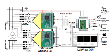
Figure 1: Proposed µPMU structure.
3. µPMU Hardware and Software Design and Implementation
In this section, the µPMU hardware design is clarified to select the appropriate components to meet the computational time and accuracy requirements including VT and CT, ADC, analog filter, GPS, and microcontroller selection. In addition, the µPMU software design to minimize the operation process within the limited time is clarified with time analysis to ensure stable operation.
3.1. Hardware Design
3.1.1 CT and VT selection
The CT and VT are used in µPMU to scale down the signal to the microcontroller level. Due to their critical rules, they are required to be of high accuracy. This is ensured by selecting a high class that meets the accuracy limits and/or robust error estimation and compensation of the CT and VT errors, which is discussed further in section 4. For the current measurements, the CT signals are transferred to a voltage by multiplying the secondary current with the secondary burden impedance. Then the voltage signal from the CT is amplified, so the 120% of the CT rate reflects the full range of the ADC voltage level. Eq.3 shows the current signal amplifier gain value.
For the proposed µPMU a CT 200/1 A-11KV, class 0.5 split core is used for the MVS, and for the LVS a CT 800/1 A-400V class 0.5 split core is used. Both CTs use 0.5-ohm pure resistance as burden impedance and the secondary voltage of both CTs have the same range. So, their current channels have the same amplifier design structure in the µPMU main measurement unit. For the voltage measurement, current-type VT is implemented by using isolating CT 1 : 1 ZMPT101B. The input voltage signal is converted to a current signal using primary side limiting resistance that is selected to limit the primary current to 2mA at the maximum input voltage. The secondary current is multiplied by the burden impedance of 0.5-ohm and the secondary voltage signal is amplified to the ADC maximum voltage level. Eq.4 represents the VT amplifier gain.
This structure provides a bi-polar voltage and current signals to the micro-controller. In regular cases, DC offset is added to shift up the sinusoidal wave above zero. However, to prevent the undefined DC offset and loading effect, which make the calibration of the unit is more difficult and less accurate as in [22], external bipolar ADC is preferred to be used to allow reading both positive and negative parts of the cycle with high accuracy. The amplifier LM324 is used, which is a general-purpose amplifier with high input resistance, linear operation and DC off-set uncertainty of 7mV.
3.1.2 ADC selection and requirements
ADC converts the analog signals of the voltage and current to digital signals to be analyzed by the microcontroller and extracts useful information from these signals. The ADC should be fast, has a linear operation mode in the operation region, and be of high resolution. Sigma-Delta, Flash, Pipeline, and Successive Approximation Registers are the four types of ADCs that are commonly used. However, SARs are the most used for general purposes due to their high accuracy, low power, zero-cycle latency, and ease to use.
In order to meet all these requirements, AD7606 SAR-type ADC is selected, which has the ability to simultaneous sampling 8-Channels-16 bits of data with a sampling frequency up to 200KHz. The AD7606 is considered as one of the best selections for DataAcquisition operation since it can operate with a 5V single supply and can accommodate a true Bipolar analog input ±5V and ±10V, with On-chip 2.5V accurate reference and reference buffer, Analog input clamp protection, Input buffer with 1 MΩ analog input impedance, Second-order anti-aliasing analog filter that has a 3 dB cutoff frequency of 15 kHz and provides 40 dB anti-alias rejection when sampling at 100 kSPS, a track-and-hold amplifier, Oversampling capability with a pin driven flexible digital filter yields improvements in Signal to Noise Ratio (SNR) to 91.2 dB, reduces the 3 dB bandwidth, and high-speed serial and parallel interfaces to communicate (Serial – Byte – Parallel) [9]. The measured value by the ADC has a resolution of 30 PPM and accuracy of ±12 LSB. Two ADCs are used to measure the 12 µPMU signals using parallel mode operation. Figure.2 shows the timing diagram to read the 12 signals within 2µsec. The following input pins are adjusted to ensure robust sampling with 512 samples/cycle:
- RANGE: Two range pins are used to control the input operating range of AD7606 (±10,±5) V range. Range Pins can be tied to either supply (±10) or to the ground (±5). In the proposed µPMU the two pins are connected to the ground for (±5) voltage operation.
- CONVERT: AD7606 has two active high Conversion start pins (A, B), one pin for start every four channels. Both the conversion pins can be tied together and controlled by a single PWM signal from the Micro Controller.
- Chip select(CS): Active low input pin, which is set to low whenever the host controller wants to perform sampling and read data.
- READ (RD/SCLK): Active low read signal is used during Parallel operation and for each pulse it will clock all the channel data out.
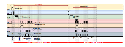
Figure 2: ADC input pins timing diagram.
3.1.3 Analog filters design
An Analog filter is used to filter the scaled signal from the CT and VT. Two low pass filters are used. The first filter removes harmonics content with a frequency above the half sampling frequency (45 − 55%fs). The second is the surge filter, which removes the transient pulses due to switching events. A second-order ButterWorth low pass filter is designed for this purpose. For the designed µPMU the cuff-off frequency of the filter is required to be in the range of 11-15 kHz, while the surge filter is designed with 100KHz. This function is made with the built-in analog filter of the selected
AD7606 with a suitable cut-off frequency for this purpose. The transfer function of the filter is estimated from the data-sheet or estimating the filter frequency gain and phase response in a lab experiment.
3.1.4 Micro-controller selection
The microcontroller is the brain of the µPMU, which organizes and controls all the hardware systems to operate correctly, calculate and send the output information. The selected microcontroller should be capable to address the minimum hardware requirements, which allows correct ADC communication, accurate and minimum time of voltage and current phasor estimation using DFT, frequency estimation and ROFC, error compensation, communication with other parts, and send the data to the PDC. Based on these requirements, STM32F407 ARM Cortex M4 ultra-high performance microcontroller is selected. STM32F407 features addressed all the minimum requirements required by the proposed µPMU specification which are:
- It provides a simultaneous conversion process.
- Samples are stored in the RAM and shared with a communication buffer through the Direct Memory Access (DMA). In the realized tests, the platform demonstrated enough processing capacity for the calculus and delivery of packages to the PDC.
- Besides that, it has an Ethernet interface, which is faster than the serial peripheral interface (SPI) and allows the data packages to transfer by directly accessing the memory via DMA without occupying the processor.
- STM32F407 is based on the high-performance Arm® Cortex®-M4 32-bit RISC core operating at a frequency of up to 168 MHz. The Cortex-M4 core features a Floating point unit (FPU) single precision which supports all Arm single-precision data-processing instructions and data types. It also implements a full set of DSP instructions and a memory protection unit (MPU) which enhances application security.
3.1.5 GPS synchronization signal and 4G communication
The µPMU measurements are synchronized with high accuracy clock from the GPS, which consists of 24 satellites in six orbits and provides a Pulse Per Second (PPS) to all GPS modules. The PPS is used in the µPMU to enable the PWM that controls the
ADC conversion process. The GPS module is selected to ensure low Synchronization Time Uncertainty (STU) to reduce the synchronization error. GPS SIM808 module is used in the proposed µPMU. The module is a GSM, GPRS, and GPS three-in-one functions module, which uses the latest GSM/GPS module SIM808 from SIMCOM, supports GSM/GPRS Quad-Band network, combines GPS technology for satellite navigation, and provides communications abilities using 4G. The GPS module has an STU of equal to 10nsec and uses different GPS and 4G antennas to mitigate the excessive communication and overlap problems.
3.1.6 µPMU Additional parts
In order to allow the useful function of the proposed µPMU, powering circuits and accessories are added to the main measurements units. First, AC/DC center-tapped pulse transformer is used to power the circuit with ±5 V. Second, the Nextion LCD touch screen is used to display the output information to the user every second. In addition, built-in storage Ultra-high-speed SD card is added to record the information with communication protocol SDIO for a period of up to 48 hours in the dynamic model. To allow the user access to the µPMU output information from the PC use, A Graphic User Interface (GUI) is designed using LabVIEW to display, save and export the output information. All hardware components are placed on a Printed Circuit Board (PCB).
3.2. Software Design
The main challenges of the designed software are to meet the time requirements of 39.06/32.55 µsec to read the 12 signals from the ADC, update the 12 phasors, and estimate the frequency and ROFC, harmonics content estimation, digital filtering, and error compensation for each updated measurements. Keeping in mind the communication time to not exceed the half-cycle.
3.2.1 Phasor estimation
Phasors play a leading role in the measurement technologies of power systems. They represent the magnitude and phase angle of the fundamental component of the voltage and current in complex representation refer to a specific time reference. DFT is used to estimate the phasor using measured ADC samples. Non-Recursive DFT estimates the phasors with previous without looking to the last estimated phasors, where DFT is applied to all 512 samples. This process required 512 × 2 product and 512 summation operation. As a result, it consumes a very large time and failed to be implemented in the proposed software structure. Recursive DFT, on the other hand, updates the new phasor based on the previous phasor estimated. This process required two multiplication and one summation process, which reduced the phasors estimation time for the proposed µPMU [23]. The estimated phasor using the Recursive method is defined by Eq. 5.
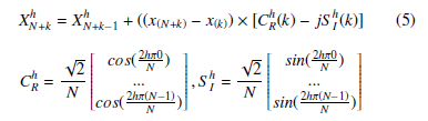
The DFT coefficient matrices CRh and S hI are precalculated and stored in the microcontroller to reduce the computational time of the DFT algorithms. It is important to note that the algorithms calculate
| XNh+k |2 to avoid the square process which consumes huge time. The angle of the phasor is measured using the linearization of tan−1 by the Tayler series described in [24]. Eq. (6) shows the phasor angle estimation using the linearization function Γ.
θN+K = Γ[Imag(XNh+k)/Re(XNh+k)] (6)
The 12 phasors estimation time is 14 µsec with these modified steps.
3.2.2 Digital filter (Simple Average Filter)
In order to compensate for the error due to leakage phenomena under the off-nominal operation, a Simple Average filter is used for both measured magnitude and angle with a window of half cycles. Therefore, the magnitude and phase of the last N/2 estimated phasor are stored in the microcontroller and the average value is calculated using Eq.(7).
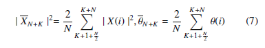
Here, | X |2 and θ are the averaged values of both magnitude power 2 and the phasor angle.
3.2.3 Frequency estimation
In order to estimate the frequency and ROFC, the angle-based method is used. In this method, the change in the phasor angle is assumed to be a quadratic time function [13, 14]. The phasor angle is stored for the last N estimated phasors and frequency defined by Eq.(8)
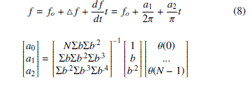
Here, b is a vector of size N, which represents the corresponding time of each sample b(n) = n/fs.In order to reduce the storage information inside the microcontroller, the b vector is precalculated and only this vector is stored in the memory. These modifications allow estimating the frequency within 2 µsec.
3.2.4 Communication Protocol
Inside the µPMU UART is used as a common communication bus to share the information between GPS, microcontroller, LCD and the directly connected PC GUI. For data export and communication with external PDC, the µPMU follows the IEEE Std C37.118.2 communication protocol to generate the data frames, uses CRC method to check this data and collect the frames in packets to send the information [15].
4. µPMU Error Estimation and Calibration
Errors are associated with the estimated phasors in each process starting from the CT and VT, analog filter, ADC sampling and digitization process, GPS synchronization, and off-nominal operation error. The output phasor calculated in this case is represented by Eq.(9)
X~ = E~CT/VT E~AFE~ADCE~GPS P~X~act (9)
where X~act is the actual phasor without error. E~CT/VT, E~AF, E~ADC, E~GPS and P~ are the complex gain error due to CT/VT scaling, analog filter error, ADC digitization error, GPS synchronization error and off-nominal complex gain P error, respectively. Each error has it is own nature and is required to be compensated, if possible, to ensure high estimation quality [13]. E~ADC and E~GPS depend on a random process and these errors are just minimized by the appropriate selection of the ADC and GPS.
4.1. CT and VT Error estimation and Compensation
CT and VT errors are external errors added to the main measurement unit of the µPMU. In traditional PMUs, CT and VT errors are small and negligible compared with the accuracy and resolution limits required by their applications. In contrast, CT and VT errors are higher in distribution since it is noisier. Also, the accuracy and resolution limits are higher in the distribution grid and transducer errors are required to be compensated to meet these limits. In this article, the CT error is the main focus, since both current and voltage measurements rely on CTs. To ensure high-quality measurements, 1) the selected CT should be of a class higher than the accuracy limits, 2) the CT error should be estimated and compensated. Two methods are existed to compensate for the CT error. In the first method, the CT is loaded under different conditions of pure and distorted input current to provide a set of experimental data. These data are used to rather define the empirical calibration equation as in [22] or learned by using an artificial neural network to compensate for the error as in [25]. In the second method, accurate modeling of the CT is used to estimate the primary current based on the CT secondary current waveform, which allows for estimating the complex gain error for the CT at different operation conditions. To achieve this, the Preisach model is used to simulate the CT B-H curve, which can represent the CT major and minor loop under different operating conditions as in [26]. For the proposed µPMU, the empirical equation is used to compensate for the CT error under steady-state. For the dynamic operation, the Discreet Preisach model is used, based on the point-on-Wave measurements provided to evaluate the CT performance under unpredicted waveform [27]. The CT and VT complex gain error estimated during the calibration is represented in Eq.(10).
E~CT/VT = I~s/I~p p.u (10)
4.2. Analog Filter Error
The analog filter error is represented by a lag phase shift and reduction in the magnitude. In order to estimate the analog filter error, the transfer function of the filter is estimated from the filter frequency and phase response in the experimental lab or from the datasheet information. Eq.(11) represents the analog filter complex gain error based on the filter parameters.
E~AF = [(1 − u2)2 + (2ζu)2]−0.5∠−Γ[(2ζu)/(1 − u2)] (11)
Here, u = 2πf/ωn, ζ and ωn are the analog filter damping coefficient and natural frequency, respectively. The analog filter error magnitude | E~AF | is linearized using Taylor series in the range of ±5 Hz to increase the algorithm’s speed and reduce the computational effort on the microcontroller.
4.3. ADC Error
The ADC error is represented by the digitization process when the sample is approximated to the nearest digital level and the sampling error. The estimated phasor is measured with samples including the digitization error. The ADC complex gain error is represented by Eq.(12).
E~ADC = [DFT(x(N+k) + γADC)]/DFT(x(N+k)) (12)
where γADC is the ADC approximation value that was added to the samples due to the digitization process. γADC is a uniform distribution function and limited between in ± half the interval between the two digital levels γADC = rand(±0.5 × LS B). The ADC error is randomly variated and can not be estimated or compensated. However, this error is reduced by using the oversampling process of the AD7606 selected in the proposed µPMU. As the number of bits increases the digitization error reduces. For the sampling error, the PWM control signal with high accuracy needs a high accuracy timer. Systick timer with 24-bit (≈ 5.95nsec) is used, which is not perfect for the required sampling frequency because for a 50Hz system the sampling time is 39.06 µsec and the timer reload value is 6562.5≥ (SystemCoreClock/1000) / (512 × 50 × 0.001). To ensure accurate sampling accumulation and deaccumulation using variable sampling interval control strategy is used [28].
4.4. GPS Error
The µPMU GPS error is represented by the module response time response to the PPS signal. The STU is defined as the maximum response time of the GPS module. The response time τ of the module is assumed to be a Gaussian Distribution function with mean and standard deviation equal to µ= 0.5STU and δ = STU/6, respectively [13]. In the proposed µPMU GPS module SIM808 module is used, which has synchronization time accuracy equals 10nsec , which gives an error in the angle of 0.00018o while GPS magnitude is approximately one. The GPS complex gain error is represented by Eq.(13), which represents a lead phase shift to the estimated phasor.
![]()
4.5. Off-nominal Error P-gain
Due to the off-nominal operation, when the frequency deviates from the nominal value, the calculated phasor is multiplied by P and Q complex gains, due to the leakage phenomena. The Q gain, which represents a second harmonics ripple, is mitigated using a simple average digital filter discussed in section 3. The complex gain P error is represented by Eq.(14).
NSin(π∆f/fs)
The P complex gain error magnitude and phase angle are linearized using Taylor series in the range of ±5 Hz to increase the algorithms speed and reduce the computational effort on the microcontroller.
4.6. White Noise
White noise is a natural error added to the measurements due to the environment and electronic distortion. Before exporting the output information, the white noise should be filtered. For this task, the Moving Average Filter (MAF) is used with a window of N/2. Eq.(15) shows the MAF representation.
where y(i − n) is the output measurements and y(i)∗ is the filtered value. Table.2 shows the error contribution of each process on the estimated phasor and the theoretical TVE estimated using Monte Carlo Simulation of 1,000,000 simulations. Transducers error shows the major contribution when they loaded by 5% of the full rate. In order to meet the accuracy limits, the developed µPMU should be calibrated against these errors and compensate for them. Figure.3 shows the µPMU processes structure and operation sequence.
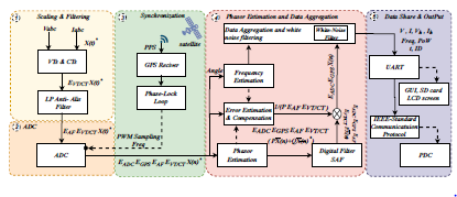
Figure 3: µPMU operation structure.
It is worth noting that in the design of the software and hardware, the measurement accuracy, software speed, and overall cost are the three main performance parameters that we care about during the design. We always looking to select the cheapest hardware that ensures the required level of accuracy with low computational time and reliable operation.
4.7. Taylor series linearization
Error compensation is an important step to improve the proposed µPMU accuracy over the previous work. However, the error compensation algorithm should be designed to be light and fast. Since the total µPMU computational time equals the sampling time, using the non-linear equations of the gain error limits the idea of error compensation. Therefore, all error gains discussed in section 4 are represented by a Taylor series. Eq.(16) shows the linearization of the complex gain error E to L order, which is mainly a function of the measured quantity d.
e is the error between the E(d) values and the linearization function.
The matrix form of the Eq. (16) for m values is represented by Eq.
Eq. (17) is solved using Least Square in Eq. (18) to find the A matrix coefficients, using D and E matrix.
A = (DT. D)−1. DT.E, m ≥ (L − 1) (18)
Using high order reduces the error e between the complex gain error and the linearization function. On the other hand, using high order increases the number of sum and multiplication operation, which increase the computational burden of the error compensation stage. Therefore, the linearization function order is selected as the smallest order to represent the complex gain error with an acceptable error range. It is important to note that for each complex gain two linearization functions are estimated for the magnitude and angle.
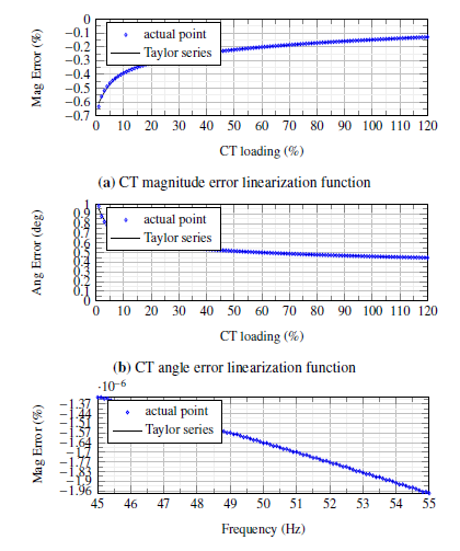
Figure.4 shows the estimated Taylor series function for the complex gain errors of the magnitude and angle for the MVS CT as an example of the power transducer, analog filter, and the complex gain P, respectively. The analog filter transfer function is estimated using the given data-sheet gain and phase frequency response. It is worth noting that there is no linearization function for the GPS error or the ADC error. Since the error produced by these elements is randomly generated, the errors of both stages are only reduced through the µPMU main measurement unit robust design such as using oversampling ADC properties, and high accuracy GPS module.
Table. 2 Shows the effect of error compensation, which shows a high improvement in the accuracy of the measurement. It is worth noting that to ensure low operation time, complex gain errors with low effect are not compensated. For example, the magnitude error due to the analog filter is very small compared with the required design limits needed. Adding error compensation for this small error, increase the computational burden on the microcontroller with the limited operation time. On the other hand, the angle error due to the analog filter is high and above the target limits of the proposed design. Therefore, analog filter angle error is considered in the error compensation stage. Gray elements in Table.2 show the error values that are required to be compensated to improve the µPMU accuracy to satisfy the target limits. Table.2 summarizes the performance of the enhancement stage, where the error compensation time reduces from 42 µsec to 0.8 µsec.
CT loading (%)
- CT magnitude error linearization function
CT loading (%)
- CT angle error linearization function
Frequency (Hz)
- SAF magnitude error linearization function
Frequency (Hz)
- SAF angle error linearization function
Frequency (Hz)
- P gain magnitude error linearization function
Frequency (Hz)
- P gain angle error linearization function Figure 4: Complex error gains linearization
5. Testing and validation
In this section, the µPMU tests are discussed according to IEEE Std C37. 118.1 and 118.2 to evaluate the main measurement unit operation and performance [14, 15]. The unit steady-state and dynamic operation is examined using six tests and the result is compared with previous work. Opal-RT simulator-OP4510 is used to generate a reference signal to the µPMU in each test and the measurements are sent to the simulator to compare and estimate the error between the two signals. Figure.5 shows the experimental setups.
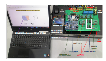
Figure 5: µPMU test and validation environment.
5.1. Steady-state tests
In steady-state operation, three tests are conducted. In the first test, the phasor magnitude estimation performance is tested in the range from 0.1-1 p.u with a variation step of 0.1 p.u. The test is made under nominal operation. In the second test, the frequency estimation performance is tested in the range of 49.5-50.5 Hz with a step change of 0.1 Hz. In the third test, the phasor angle estimation performance is tested using input signals with phase shifts 1, 0.1, and 0.01 degrees to estimate the angle accuracy and resolution.
5.2. Dynamic tests
In dynamic operation, three tests are conducted to test the performance of the µPMU under dynamic operation. In the first test, an input signal with a ramp frequency change of 0.2 Hz/sec is applied to the µPMU, the main purpose of this test is to evaluate the performance of estimating the ROFC and frequency. In the second test, two input signals are applied to the µPMU, one with a sudden change by 0.1 p.u and 10 degrees to estimate the phasor step response of the µPMU and the other signal with a step frequency change by ± 0.5 Hz to estimate the frequency step response. In the third test, a sinusoidal wave of fundamental and 40% harmonics is measured by the proposed µPMU. The test is made for harmonics content up to 16th harmonic order. The µPMU is adjusted to operate on the dynamic mode to provide the point-on-wave measurement in this test. The main purpose of this test is to check the performance of the µPMU to estimate the harmonics content of the input signal and shows the point-on-wave data.
Table 2: Theoretical error limits using MCS and Taylor linearization performance
|
|||||||||||||||||||||||||||||||||||||||||||||||||||||||||||||||||||||||||||||||||||||||||||||||||||||||||||||||||||||
6. Result and Discussion
In this section the performance of the proposed µPMU is analyzed under the standard tests of IEEE- C37.118.1 and C37.118.2 is discussed.
6.1. Steady-state operation
6.1.1 Test1 (Magnitude step change)
The result of the magnitude step change is shown in Figure.6. The magnitude estimation under nominal operation shows a very accurate result, the TVE is 0.0318% including the current-type VT without error compensation. The bipolar structure shows more stability and less error compared with adding DC off-set as in [22]. The error in the estimated frequency showed a mean of 3.5 mHz and a standard deviation in the measurement of 1mHZ, which resulted in a maximum variation of 6mHz in a transient change in the voltage. However, compared with previously designed units in the literature the proposed µPMU shows lower variations.
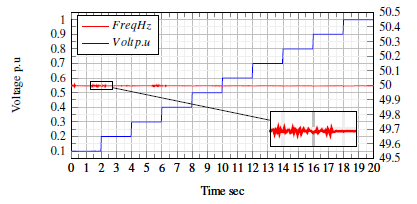
Figure 6: Magnitude step change.
6.1.2 Test2 (Frequency step change)
The result of the frequency step change is shown in Figure.7. The magnitude estimation under off-nominal operation shows degradation in the accuracy. For the magnitude, the TVE increased to 0.7% at the transition period shown by pulses in the graph. Otherwise, the TVE is less than 0.05%. The error in the estimated frequency showed a maximum variation of 0.1 Hz at the transient change, while inside the range stable operation, the frequency maximum variation is 30 mHz. The increased error in both the magnitude and frequency happened due to the off-nominal operation complex gain error P and Q.
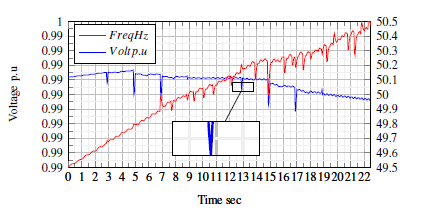
Figure 7: Frequency step change.
6.1.3 Test3 (Angle accuracy and resolution)
Three signals with a phase shift of 1, 0.1, and 0.01 degrees are applied to the µPMU channel. Figure.8 shows the measured angle in all tests. In the three cases, the µPMU showed robust estimation. The mean of the error is constant in the three cases and has a mean of 0.0036o lag phase shift, due to the analog filter and the complex gain P, and a very low standard deviation equals 2.85o × 10−5. The µPMU angle resolution detected is 0.0036 degrees and reflects the ADC resolution with a sampling frequency of 512 samples/cycle.
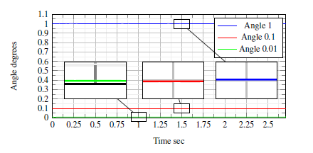
Figure 8: Angle variation.
6.2. Dynamic Operation
6.2.1 Test4 (Ramp frequency change)
When the ramp signal is applied to the µPMU, the estimated ROFC equals the input signal value of 0.2HZ. Figure.9 shows the reported estimated frequency during the test. At the nominal region, the frequency has low ripple and low error, as the frequency deviated with time (increase or decrease), the off-nominal caused a deviation in the measured frequency. As the difference from the nominal frequency increases, the deviation of the measured frequency also increases due to the mismatch of the analog filter and the off-nominal error due to P and Q complex gain frequency.
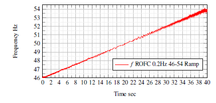
Figure 9: Ramp frequency change.
6.2.2 Test5 (Phasor and frequency step response)
In the case of phasor step change, the phasor magnitude and the angle have the same TVE, accuracy, and resolution in the steadystate. Both magnitude and phase response to the change at the same time and have a response time of 20 msec, which represents the reporting rate and it is also equal to the µPMU latency as shown by Figure.10. This value depends on the selected reporting rate due to the operation mode and can be reduced by adjusting the reporting rate of 2 measurements/cycle. In the case of frequency step change by ± 0.5 Hz, at the nominal operation, the variation of the measured frequency is within the range of 4 mHz, which results in a TVE of 0.008%. The frequency of the two signals is changed with a step of ± 0.5Hz and 49.5, which causes off-nominal operation. Therefore, the second harmonics ripple is added to the measured phasor causing a second harmonics to change in the angle and frequency. The SAF mitigates this ripple to a final variation of ± 16 mHZ. Figure.11 shows the reported frequency measurements.
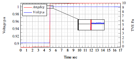
Figure 10: Phasor step response.
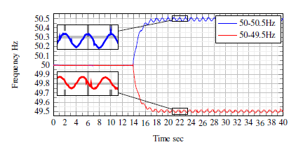
Figure 11: Frequency step response.
6.2.3 Test6 (Harmonics content)
In this test, a sinusoidal wave of 60% fundamental and 40% harmonics from 2nd-16th order is measured by the µPMU. Figure.12 represents the point-on-wave data recorded of the first four signals. Figure.13 the p.u error in the estimated harmonics is shown. The maximum error is found to be 1.36% in the 6th harmonics. In all harmonics, the error is around 1.206%. This magnitude shift is made by the amplifier LM324 DC shift and uncertainty in the gain, which could be improved by using a better amplifier in future design. Table.3 shows a comparison between the proposed unit previous proposed units.
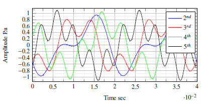
Figure 12: Harmonics Point-on-wave data 2nd-5th.
- 10−2
Harmonics order
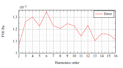
Figure 13: Harmonics estimation error.
Table 3: Comparison of µPMUs
|
|||||||||||||||||||||||||||||||||||||||||||||||||||||||||||||||||||||||||||||||||||||||||||
7. Conclusion
This article presents a roadmap to design distribution level µPMU to meet the requirements of distribution grid applications. The µPMU hardware and software are discussed to ensure the robust design and minimum software operation time. Proposed µPMU shows accurate performance during steady-state and dynamics operation and meets their application requirements with an accuracy and resolution up to 1% and 0.1% for the magnitude and 0.1o and 0.01o for the angle. The proposed µPMU address the required limits with a phasor estimation accuracy up to 0.03% for the magnitude and 0.0036 angle resolution, while the frequency is estimated with accuracy up to 0.006% under steady-state. For dynamic operation, both phasor and frequency measurements show a certain level of degradation due to the dynamic and off-nominal error. Power system frequency variation shows a higher effect over magnitude and phase variation. The magnitude and frequency of TVE are degraded to 0.05% and 0.032% under dynamic operation, while the angle variation is the same for both cases. By using linearization, the off-line calculation time is reduced to 18µsec, which allows stable communication. The overall µPMU performance addressed the required specification and showed robust performance under steady-state and dynamic operation.
Acknowledgment
This work was done as part of the research project “ Smart Monitoring system for Distribution Power Grid ” supported by the Egyptian National Telecom Regulatory Authority (NTRA). Also, the authors would like to thank the Smart-Systems Company for providing the real-time simulator and the µPMU test environment.
- J. A. Momoh, Smart grid: fundamentals of design and analysis, volume 63, John Wiley & Sons, 2012.
- A. Von Meier, E. Stewart, A. McEachern, M. Andersen, L. Mehrmanesh, “Precision micro-synchrophasors for distribution systems: A summary of appli-
cations,” IEEE Transactions on Smart Grid, 8(6), 2926–2936, 2017. - F. C. Trindade, W. Freitas, “Low voltage zones to support fault location in distribution systems with smart meters,” IEEE Transactions on Smart Grid, 8(6), 2765–2774, 2016.
- P. De Oliveira-De Jesus, C. H. Antunes, “Economic valuation of smart grid investments on electricity markets,” Sustainable Energy, Grids and Networks, 16, 70–90, 2018.
- X. Zhao, D. M. Laverty, A. McKernan, D. J. Morrow, K. McLaughlin, S. Sezer, “GPS-disciplined analog-to-digital converter for phasor measurement applica- tions,” IEEE Transactions on Instrumentation and Measurement, 66(9), 2349– 2357, 2017.
- D. Dotta, J. H. Chow, D. B. Bertagnolli, “A teaching tool for phasor measure- ment estimation,” IEEE Transactions on Power Systems, 29(4), 1981–1988, 2014.
- A. Singh, S. Parida, “Power System Frequency and Phasor Estimation for Low-Cost Synchrophasor Device Using Non-Linear Least Square Method,” IEEE Transactions on Industry Applications, 2021.
- T. Ahmad, N. Senroy, “Statistical characterization of PMU error for robust WAMS based analytics,” IEEE Transactions on Power Systems, 35(2), 920– 928, 2019.
- D. Schofield, F. Gonzalez-Longatt, D. Bogdanov, “Design and implementation of a low-cost phasor measurement unit: A comprehensive review,” in 2018 Seventh Balkan Conference on Lighting (BalkanLight), 1–6, IEEE, 2018.
- M. C. Garcia, D. Dotta, L. Pereira, M. C. de Almeida, M. R. Paternina, O. L. dos Santos, L. C. da Silva, J. E. d. R. A. Junior, “A development PMU device for living lab applications,” Journal of Control, Automation and Electrical Systems, 32(4), 1111–1122, 2021.
- M. C. Garcia, D. Dotta, L. Pereira, M. C. de Almeida, O. L. Santos, L. C. da Silva, “Design and development of D-PMU module for smart meters,” in 2020 IEEE Power & Energy Society General Meeting (PESGM), 1–5, IEEE, 2020.
- R. N. Rodrigues, L. H. Cavalcante, J. K. Zatta, L. C. M. Schlichting, “A Phasor Measurement Unit based on discrete fourier transform using digital signal pro- cessor,” in 2016 12th IEEE International Conference on Industry Applications (INDUSCON), 1–6, IEEE, 2016.
- P. Romano, M. Paolone, T. Chau, B. Jeppesen, E. Ahmed, “A high-performance, low-cost PMU prototype for distribution networks based on FPGA,” in 2017 IEEE Manchester PowerTech, 1–6, IEEE, 2017.
- PSL, “Micro-PMU Datasheet,” in [Online], Avail- able:https://powerside.com/wpcontent/uploads /2020/01/Powerside-t-.pdf, Accessed on: Aug.1, 2021.
- A. A. E. Elsayed, M. A. Mohamed, M. A. Nayel, “Distribution Grid Phasor Estimation and µPMU Modeling,” in 2022 IEEE International Conference on Power Electronics, Smart Grid, and Renewable Energy (PESGRE), 1–8, IEEE, 2022.
- I. Power, et al., “IEEE Standard for Synchrophasor Measurements for Power Systems–Amendment 1: Modification of Selected Performance Requirements,” IEEE Std C37. 118.1 a-2014 (Amendment to IEEE Std C37. 118.1-2011), 2014, 1–25, 2014.
- IEEE, “IEEE standard for synchrophasor data transfer for power systems,” IEEE Standard C37. 118.2-2011 (Revision of IEEE Std C37. 118-2005), 1–53, 2011.
- NASPI, “Distribution Synchronized Measurements Roadmap Final Report,” in [Online], https://www.naspi.org/node/934, Accessed on: Apr.15, 2022.
- J. Zhao, G. Zhang, “A robust prony method against synchrophasor measurement noise and outliers,” IEEE Transactions on Power Systems, 32(3), 2484–2486, 2016.
- A. G. Phadke, J. S. Thorp, “Phasor measurement units and phasor data con- centrators,” in Synchronized Phasor Measurements and Their Applications, 83–109, Springer, 2017.
- “IEEE Draft Recommended Practices and Requirements for Harmonic Control in Electric Power Systems,” IEEE P519/D6ba, September 2013, 1–26, 2013.
- A. A. E. Elsayed, M. A. Mohamed, M. Abdelraheem, M. A. Nayel, “Optimal
µPMU Placement Based on Hybrid Current Channels Selection for Distribution Grids,” IEEE Transactions on Industry Applications, 56(6), 6871–6881, 2020. - A. A. Elaziez, M. A. Mohamed, M. AbdelRaheem, M. A. Nayel, “Optimal µPMU placement and current channel selection considering running cost for distribution grid,” in 2020 IEEE International Conference on Power Electronics, Smart Grid and Renewable Energy (PESGRE2020), 1–8, IEEE, 2020.
- I. Abubakar, S. Khalid, M. Mustafa, H. Shareef, M. Mustapha, “Calibration of ZMPT101B voltage sensor module using polynomial regression for accu- rate load monitoring,” Journal of Engineering and Applied Sciences, 12(4), 1077–1079, 2017.
- A. G. Phadke, J. S. Thorp, Synchronized phasor measurements and their appli- cations, volume 1, Springer, 2008.
- G. Daoud, H. Selim, M. M. AbdelRaheem, “Micro phasor measurement unit phasor estimation by off-nominal frequency,” in 2018 IEEE International Con- ference on Smart Energy Grid Engineering (SEGE), 53–57, IEEE, 2018.
- M. S. Ballal, M. G. Wath, H. M. Suryawanshi, “A novel approach for the error correction of CT in the presence of harmonic distortion,” IEEE Transactions on Instrumentation and Measurement, 68(10), 4015–4027, 2018.
- A. Rezaei-Zare, R. Iravani, M. Sanaye-Pasand, H. Mohseni, S. Farhangi, “An accurate current transformer model based on Preisach theory for the analysis of electromagnetic transients,” IEEE Transactions on Power Delivery, 23(1), 233–242, 2007.
- M. Andreev, A. Suvorov, N. Ruban, R. Ufa, A. Gusev, A. Askarov, A. Kievets, “Development and research of mathematical model of current transformer re- producing magnetic hysteresis based on Preisach theory,” IET Generation, Transmission & Distribution, 14(14), 2720–2730, 2020.
- W. Yao, L. Zhan, Y. Liu, M. J. Till, J. Zhao, L. Wu, Z. Teng, Y. Liu, “A novel method for phasor measurement unit sampling time error compensation,” IEEE Transactions on Smart Grid, 9(2), 1063–1072, 2016.
No related articles were found.