
NiO Quantum dots Doped Triple Cation Perovskite Cs MAFAPb I2Br2 Heterojunction Photodetector with High Responsivity
Volume 7, Issue 3, Page No 161-165, 2022
Author’s Name: Yara Abdullah Alwadei1, Manar Saleh Alshatwi2,a), Norah Mohammed Alwadai2, Maymunah Abdullah AlWehaibi2, Mohammad Faihan Alotaibi3, Maha Mahmoud Lashin4, Mohammad Hayal Alotaibi3
View Affiliations
1 Manarat-Alriyadh Schools, P.O. Box 3835, Riyadh 1148, Saudi Arabia
2 Department of Physics, College of Sciences, Princess Nourah bint Abdulrahman University, P.O. Box 84428, Riyadh 11671, Saudi Arabia
3 National Center for Nanotechnology, King Abdulaziz City for Science and Technology, P.O. Box 6086, Riyadh 11442, Saudi Arabia
4 College of Engineering, Princess Nourah bint Abdulrahman University, P.O. Box 84428, Riyadh 11671, Saudi Arabia
a)whom correspondence should be addressed. E-mail: Manarsalleh@gmail.com
Adv. Sci. Technol. Eng. Syst. J. 7(3), 161-166 (2022); ![]() DOI: 10.25046/aj070318
DOI: 10.25046/aj070318
Keywords: Photodetectors, Organic–inorganic perovskites, Quantum Dots, NiO, Responsivity, Heterojunction

Export Citations
Optoelectronic devices applications based on Organic–inorganic perovskites are promising and effective low-cost energy materials due to their exceptional physical properties which include high carrier mobility, high optical absorption coefficient, and long carrier diffusion length. In the presented work, a TiO2/NiO+5% Fe quantum dots (QDs)–doped CsMAFAPbI2Br2 perovskite heterojunction broadband photodetector was fabricated on FTO/glass substrate. The photodetector can detect a wide range of wavelengths, from UV to Vis (100–800 nm), has high responsivity (0.99 A/W), and has excellent detectivity (8.9 × 10¹² Jones). Scanning electron microscopy (SEM), transmission electron microscopy (TEM), X-ray diffraction (XRD), atomic force microscopy (AFM), and electrical (I–V) characterization were used to measure the responsivity and detectivity of the photodetectors. Doping with NiO+5% Fe QDs protected the device from oxygen and moisture and improved the morphology of the perovskite by reducing pit defects. The results showed high performance and the potential of a NiO+5% Fe QDs–doped triple cation perovskite photodetector device.
Received: 13 March 2022, Accepted: 04 June 2022, Published Online: 27 June 2022
1. Introduction
In the last decade, hybrid organic–inorganic perovskites (HOIPs) have attracted significant attention because of their chemical variability, structural diversity, and favorable physical properties. HOIPs can be classified into formates, azides, dicyanamides, cyanides, and dicyanometallates. They are a future material for optoelectronic applications [1], optical communication, light-emitting diodes [2], UV detectors [3], gas sensors [4], transistors [5], and solar cells [6]. HOIPs have 400–990 nm coefficient of absorption, long carrier diffusion lengths, and high carrier mobilities [6]. ABX3 is the main perovskite structure. Within the formula ABX3, A is an organic or inorganic cation, usually methylammonium CH3NH3+, formamidinium CH2(NH2)2+, FA, Cs+, or Rb+; B is Pb2 or Sn2; and X is a halide anion or mixed halide (to gain stability and resistance to environmental influence). The formula ABX3 is illustrated in figure 1.
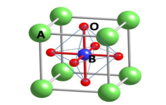
Figure 1: The structure of perovskite.
Varieties of perovskites have been developed via different preparation procedures, varying properties such as the choice of cations or halide elements, and optimizing the morphology. Perovskites with mixed cations and halides have been more thermally and structurally stable than pure perovskites. One of the most efficient mixtures of cations and halides is triple cation perovskite CsFAMA, which is currently a promising material for future optoelectronic applications. Triple cation perovskite CsFAMA has high thermal stability, reduced recombination, and increased electron lifetime due to a low percentage of Cs, resulting in highly homogenous grains of pure perovskite [6]. Moreover, partially displacing inorganic cations, such as Cs+ and Rb+, enhances the thermal and mechanical stability of MA/FA halide perovskites. The stability and distortion of a crystal perovskite material’s structure can be estimated by finely controlling the t value. By combining organic cations, such as FA or MA, with relatively slight amounts of Rb+ or Cs+ cations, a more beneficial Goldschmidt tolerance factor (t) value can be achieved, allowing the photoactive perovskite phase to be stabilized over a wider temperature range, leading to stable devices [7–9]. The development of stable and efficient electron transport materials (ETM) and hole transport materials (HTM) is of prime consideration. Heterojunction photodetectors can be produced using metal oxides, such as ZnO, TiO2, WO2, or SnO2, as an electron transport layer (ETL). Triple cation perovskite CsFAMA photodetectors have high-density pits defects, which have the effect of reducing carrier transport, reducing responsivity, and decreasing the crystal quality of the film. Fe doped NiO improves the properties of carrier transport due to better transmission, wide band gap, high stability, and suitable alignment of energy level with perovskite for good hole collection [10–13]. In the presented work, we demonstrate the enhancement of the responsivity and detectivity of triple cation perovskite photodetectors by optimizing the morphology. This is done through fabricated heterojunction photodetectors by doping with iron-doped nickel oxide quantum dots (QDs).
2. Experiment
2.1 Preparation of CsMAFAPbI2Br2
Using a glove box, a mix of 21.84 mg of CsI, 18.84 mg of MABr2 , 62.04 mg of PbBr2 , 247.2 mg of FAI, and 722.4 mg of PbI2 was dissolved in anhydrous dimethylformamide/dimethylsulphoxide at a 4:1 volume ratio to create a perovskite precursor solution.
2.2 Preparation of spiro-OMeTAD
HTM solutions were prepared in a N2 glove box by mixing 17.8 µL of lithium (Li) with 28.8 µL of 4-Tert-Butylpylpyridine and then adding 85.6 mg of spiro-OMeTAD with 1000 µL chlorobenzene.
2.3. Preparation of Iron-doped NiO Quantum Dots
Chemical precipitation is the normal method for preparing QDs. In this study, iron-doped NiO QDs synthesized by dissolving 13.81 g nickel nitrate, Ni (NO3)2, and 1.01 g iron nitrate, Fe (NO3)3, in 50 mL of distilled water at a moderate stirring speed at 50°C. After 15 minutes, 1 g of citric acid was added to the mixture, and it was stirred for another 15 minutes. Then, a drop of ammonium hydrate was added, and precipitate began to form until the combination became a thick gel. The temperature was eventually elevated to obtain a totally dry sample, producing FeO3-doped NiO QDs. Finally, the samples were heated for 2 hours at 350°C in a furnace.
2.4. Thin films and photodetector fabrication
Ultrasonication in deionized water, acetone, and ethanol was used to clean the fluorine-doped tin oxide (FTO) / glass substrate, followed by UV drying for 15 minutes. Then, a nanoscale blocking layer (TiO2) was sprayed on the cleaned FTO at 450°C (1:9 volume ratio) using a commercial titanium diisopropoxide bis (acetylacetonate) solution (75% in 2-propanol, Sigma-Aldrich) diluted in anhydrous ethanol. A 150 nm TiO2 mesoporous layer was spin coated at 4000 rpm for 20 seconds then annealed at 450°C for 30 minutes in dry air (diluted paste, 1:6 wt. ratio of Dyesol 30NRD to ethanol). Manufacturing of the device was done inside a dry air box under carefully controlled settings. In a two-stage process, Spin coating of perovskite solution at 1000 and 6000 rpm was performed. Iron-doped NiO QDs were doped within the perovskite at the same stage. On the spinning substrate, 200 µL of chlorobenzene was dropped in the last 10 seconds of spinning. All samples were annealed at 100°C for 45 minutes. Finally, spiro-OMeTAD was coated as hole transport layer in steps at 4000 rpm for 20 seconds, as shown in figure 2.
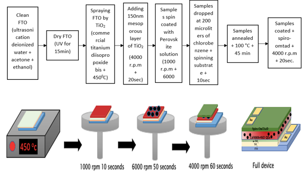
Figure 2. (a) Steps of photodetector fabrication.
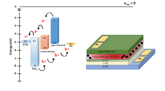
Figure 2. (b) band gap alignment
3. Results and Discussion
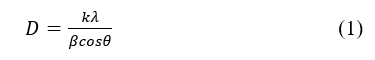
SEM imaging was used for studying the manufactured NiO+5%Fe QDs–doped triple cation CsMAFAPbI2Br2 film. Figure 3(a) shows a NiO+5% Fe QDs image where the QDs are nearly spherical with 4.3, 5.6, 9.7, and 11.6 nm sizes. A CsMAFAPbI2Br2 perovskite film exhibiting many voids and defects between grains is shown in figure 3(b). Doping NiO+5% Fe in the perovskite surface improved morphology and decreased defects. A cross section of the device and image of NiO+5% Fe QDs is shown in figure 3(c). Figure 3(d),(e) shows high-resolution TEM (HR-TEM) images of NiO+5% Fe QDs in different scales.
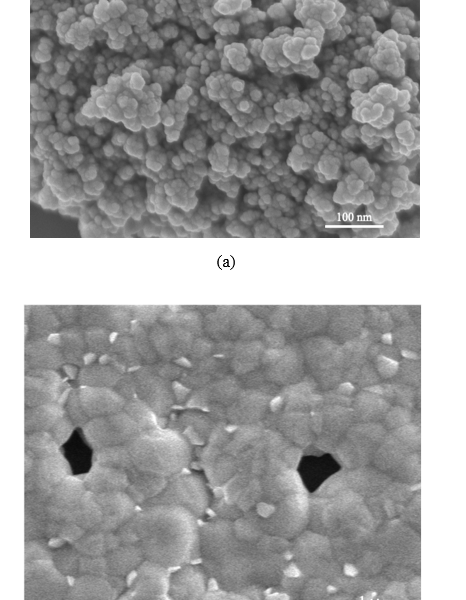
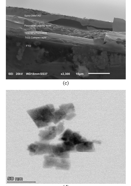
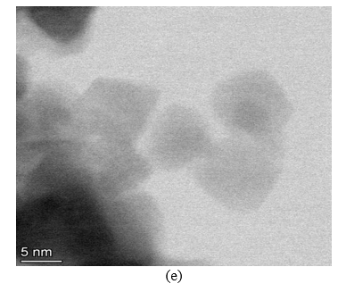
Figure 3. (a) SEM image of NiO+5% Fe QDs calcined at 350 °C. (b) Illustration of morphology of CsFAMAPbI2Br2 perovskite. (c) Cross section of full device. (d) HR-TEM images of NiO+5% Fe QDs.
NiO+5% Fe QDs with 5 nm particle size, with XRD that doped NiO+5% Fe QDs by CsMAFAPbI2Br2 and SEM homogeneously distribution, as shown in figure 4(a). The diffraction peaks were observed at 37.2°, 43.1°, 62.90°, 74.9°, and 79.2° for the NiO+5% Fe QDs that were well-defined for (111), (200), (220), (311), and (222) cubic NiO3+FeO3 crystals [14,15].The CsMAFAPbI2Br2 /NiO+5% Fe film confirmed the formation of α-Fe2O3 phase via the observed peaks (024) and (116) at 50.4° and 52.2°, respectively, which is consistent with previous studies [16,17]. The diffraction peaks of CsMAFAPbI2Br2 were observed at 12.5°, 19.8°, 24.3°, 28.2°, 31.6°, 34.7°, 40.3°, 42.9°, 49.8°, 60.3°, and 73.2° for (011), (002), (211), (100), (111), (224), (024), (166), (220), and (311), respectively, confirming the diffraction pattern of the cubic perovskite. The NiO3+FeO3 QDs size derived from the diffraction peaks using the Scherrer formula was 5.6 nm. The Scherrer formula can be written as follows:
where D is the crystallite size, k = 0.89 is the Scherrer constant depend on the spherical particles and crystals index (hkl), λ= 0.145 is the source wavelength, and β is the full width at half the maximum (FWHM) of the peak in radians.
AFM topography maps of 5 μm CsMAFAPbI2Br2 perovskite films are shown in figure 4(b). The maps identified a slightly uniform grain distribution with dimensions between 200 and 400 nm and created a unified background film with pit defects, and comparable dimensions, surpass in height and exhibit a morphological contrast on the background layer’s surface. The CsMAFAPbI2Br2 perovskite film’s thickness was assessed as 372 nm ± 31, which is similar to the grains’ lateral dimensions.
Studies of UV absorption show a blue shift. Figure 5(a) shows the absorption spectra and a decrease in bandgap as a result of an increase in QD size. The UV absorption spectrum’s peaks were between 300 and 400 nm, which is consistent with previous research [18,19]. CsMAFAPbI2Br2 absorption peaks found between 700 and 800 nm in the visible region is consistent with previous studies [20]. Figure 5(b) shows the absorption of CsMAFAPbI2Br2 doped with NiO QDs in the broadband visible, and the absorption spectrum from UV to visible is shown in figure 5(c).
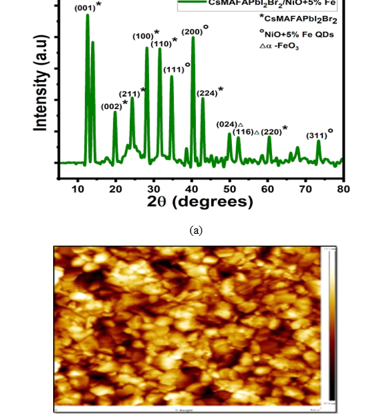
Figure 4.(a)CsMAFAPbI2Br2 /NiO+5% Fe XRD patterns. (b) CsMAFAPbI2Br2 AFM image
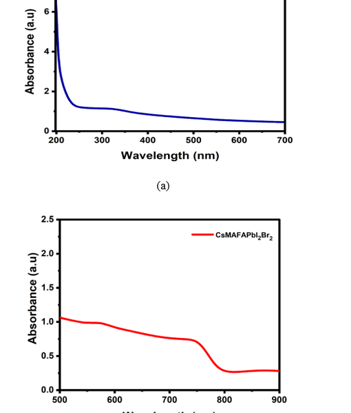
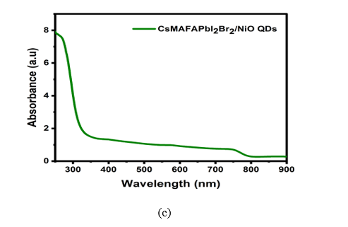
Figure 5. UV–visible absorption spectra of (a) NiO QDs, (b)CsMAFAPbI2Br2 , and (c) NiO QDs/CsMAFAPbI2Br2 .
Current–voltage (I–V) measurements of NiO+5% Fe QDs–doped CsMAFAPbI2Br2 were measured under dark conditions and illumination with 1 mW/m2. The performance of the photodetector NiO+5% Fe QDs device is shown in figure 6(a). Equation (2) were used for calculating a photo-responsivity (R) where denotes the difference between the photo-current and the dark current, denotes incident power density, and denotes the effective area illuminated by the white lamp source. Furthermore, we calculated the detectivity ( ) by equation (3) where denotes the electron charge ( ) and denotes the dark current density. R and D* were calculated depend on that noise in the current noise is mainly dominated by shot noise. Compared with a previous study [21] appeared responsivity 0.99 A/W where the detectivity of 8.9 × 10¹² Jones, related to the improved morphology with a decrease in grain size and vacancies, which is reflected in the high performance level of our photodetector. By using on/off ratio as a measurement of photodetector repeatability, we obtained a high capacity that allows the photodetector to be operated repeatedly and with the same efficiency without any damage to the photodetector, as shown in figure 6(b).
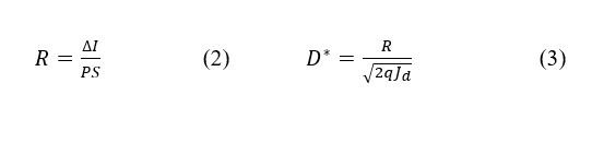
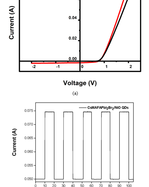
Figure 6. (a) I–V characteristics of CsMAFAPbI2Br2 photodetector heterojunction under illumination of 1 mW/m2. (b) On/off ratio of CsMAFAPbI2Br2/NiO+5% Fe QDs photodetector heterojunction.
4. Conclusion
In the presented work, our goals were achieved with enhanced responsivity and detectivity of the photodetector while trying to keep a low dark current. Doping NiO QDs in the perovskite layer significantly reduced perovskite pit defects. The responsivity of the photodetector was enhanced by 47% (0.99 A) with doped NiO+5% Fe QDs and a detectivity of 8.9 × 10¹² Jones was achieved, which is the highest value that has been reported. Moreover, the photodetector performance was enhanced by expanding the photodetection range from the UV to the visible spectrum.
Acknowledgement
The authors express their gratitude to Princess Nourah bint Abdulrahman University Researchers Supporting Project (Grant No. PNURSP2022R11), Princess Nourah bint Abdulrahman University, Riyadh, Saudi Arabia. This work was supported by King Abdulaziz City for Science and Technology (KACST).
- S. Xu, Y. Qin, C. Xu, Y. Wei, R. Yang, Z.L. Wang, “Self-powered nanowire devices,” Nature Nanotechnology, 5(5), 2010, doi:10.1038/nnano.2010.46.
- B.O. Jung, Y.H. Kwon, D.J. Seo, D.S. Lee, H.K. Cho, “Ultraviolet light emitting diode based on p-NiO/n-ZnO nanowire heterojunction,” Journal of Crystal Growth, 370, 2013, doi:10.1016/j.jcrysgro.2012.10.037.
- S.S. Shinde, K.Y. Rajpure, “Fabrication and performance of N-doped ZnO UV photoconductive detector,” Journal of Alloys and Compounds, 522, 2012, doi:10.1016/j.jallcom.2012.01.118.
- R. Bao, C. Wang, L. Dong, R. Yu, K. Zhao, Z.L. Wang, C. Pan, “Flexible and controllable piezo-phototronic pressure mapping sensor matrix by ZnO NW/p-polymer LED array,” Advanced Functional Materials, 25(19), 2015, doi:10.1002/adfm.201500801.
- M. Esro, G. Vourlias, C. Somerton, W.I. Milne, G. Adamopoulos, “High-mobility ZnO thin film transistors based on solution-processed hafnium oxide gate dielectrics,” Advanced Functional Materials, 25(1), 2015, doi:10.1002/adfm.201402684.
- S. Ašmontas, A. Čerškus, J. Gradauskas, A. Grigucevičienė, K. Leinartas, A. Lučun, K. Petrauskas, A. Selskis, A. Sužiedėlis, E. Širmulis, R. Juškėnas, “Cesium-containing triple cation perovskite solar cells,” Coatings, 11(3), 2021, doi:10.3390/coatings11030279.
- R.E. Beal, D.J. Slotcavage, T. Leijtens, A.R. Bowring, R.A. Belisle, W.H. Nguyen, G.F. Burkhard, E.T. Hoke, M.D. McGehee, “Cesium Lead Halide Perovskites with Improved Stability for Tandem Solar Cells,” Journal of Physical Chemistry Letters, 7(5), 2016, doi:10.1021/acs.jpclett.6b00002.
- Y. Hu, E.M. Hutter, P. Rieder, I. Grill, J. Hanisch, M.F. Aygüler, A.G. Hufnagel, M. Handloser, T. Bein, A. Hartschuh, K. Tvingstedt, V. Dyakonov, A. Baumann, T.J. Savenije, M.L. Petrus, P. Docampo, “Understanding the Role of Cesium and Rubidium Additives in Perovskite Solar Cells: Trap States, Charge Transport, and Recombination,” Advanced Energy Materials, 8(16), 2018, doi:10.1002/aenm.201703057.
- Y. Hu, M.F. Aygüler, M.L. Petrus, T. Bein, P. Docampo, “Impact of Rubidium and Cesium Cations on the Moisture Stability of Multiple-Cation Mixed-Halide Perovskites,” ACS Energy Letters, 2(10), 2017, doi:10.1021/acsenergylett.7b00731.
- X. Yin, M. Que, Y. Xing, W. Que, “High efficiency hysteresis-less inverted planar heterojunction perovskite solar cells with a solution-derived NiOx hole contact layer,” Journal of Materials Chemistry A, 3(48), 2015, doi:10.1039/c5ta08193a.
- J. Cui, F. Meng, H. Zhang, K. Cao, H. Yuan, Y. Cheng, F. Huang, M. Wang, “CH3NH3PbI3-based planar solar cells with magnetron-sputtered nickel oxide,” ACS Applied Materials and Interfaces, 6(24), 2014, doi:10.1021/am507108u.
- I.J. Park, G. Kang, M.A. Park, J.S. Kim, S.W. Seo, D.H. Kim, K. Zhu, T. Park, J.Y. Kim, “Highly Efficient and Uniform 1 cm2 Perovskite Solar Cells with an Electrochemically Deposited NiOx Hole-Extraction Layer,” ChemSusChem, 10(12), 2017, doi:10.1002/cssc.201700612.
- X. Yin, J. Liu, J. Ma, C. Zhang, P. Chen, M. Que, Y. Yang, W. Que, C. Niu, J. Shao, “Solvothermal derived crystalline NiOx nanoparticles for high performance perovskite solar cells,” Journal of Power Sources, 329, 2016, doi:10.1016/j.jpowsour.2016.08.102.
- P.M. Ponnusamy, S. Agilan, N. Muthukumarasamy, T.S. Senthil, G. Rajesh, M.R. Venkatraman, D. Velauthapillai, “Structural, optical and magnetic properties of undoped NiO and Fe-doped NiO nanoparticles synthesized by wet-chemical process,” Materials Characterization, 114, 2016, doi:10.1016/j.matchar.2016.02.020.
- K. Karthik, G.K. Selvan, M. Kanagaraj, S. Arumugam, N.V. Jaya, “Particle size effect on the magnetic properties of NiO nanoparticles prepared by a precipitation method,” Journal of Alloys and Compounds, 509(1), 2011, doi:10.1016/j.jallcom.2010.09.033.
- M. Qayoom, K.A. Shah, A.H. Pandit, A. Firdous, G.N. Dar, “Dielectric and electrical studies on iron oxide (α-Fe2O3) nanoparticles synthesized by modified solution combustion reaction for microwave applications,” Journal of Electroceramics, 45(1), 2020, doi:10.1007/s10832-020-00219-2.
- S. Suresh, S. Karthikeyan, K. Jayamoorthy, “Effect of bulk and nano-Fe2O3 particles on peanut plant leaves studied by Fourier transform infrared spectral studies Effect of Fe2O3 particles on peanut plant leaves >,” Journal of Advanced Research, 7(5), 739–747, 2016, doi:10.1016/j.jare.2015.10.002.
- P.A. Sheena, K.P. Priyanka, N. Aloysius Sabu, S. Ganesh, T. Varghese, “Effect of electron beam irradiation on the structure and optical properties of nickel oxide nanocubes,” Bulletin of Materials Science, 38(4), 2015, doi:10.1007/s12034-015-0953-5.
- T. Singh, T. Miyasaka, “Stabilizing the Efficiency Beyond 20% with a Mixed Cation Perovskite Solar Cell Fabricated in Ambient Air under Controlled Humidity,” Advanced Energy Materials, 8(3), 2018, doi:10.1002/aenm.201700677.
- S. Tong, C. Gong, C. Zhang, G. Liu, D. Zhang, C. Zhou, J. Sun, S. Xiao, J. He, Y. Gao, J. Yang, “Fully-printed, flexible cesium-doped triple cation perovskite photodetector,” Applied Materials Today, 15, 2019, doi:10.1016/j.apmt.2019.03.001.
- G.R. Adams, V.O. Eze, M.A.S. Shohag, R. Simpson, H. Parker, O.I. Okoli, “Fabrication of rapid response self-powered photodetector using solution-processed triple cation lead-halide perovskite,” Engineering Research Express, 2(1), 2020, doi:10.1088/2631-8695/ab7b38.