
A CMOS On-Chip High-Precision PVTL Detector
Volume 7, Issue 3, Page No 87-94, 2022
Author’s Name: Pang-Yen Lou1, Ying-Xuan Chen1, Chua-Chin Wang1,a), Wei-Chih Chang2
View Affiliations
1National Sun Yat-Sen University, Department of Electrical Engineering, 70 Lian-Hai Rd., Kaohsiung, Taiwan
2FocalTech Systems Co., Ltd, 6, Du Sing 1st Rd, East District, Hsinchu, Taiwan
a)whom correspondence should be addressed. E-mail: ccwang@ee.nsysu.edu.tw
Adv. Sci. Technol. Eng. Syst. J. 7(3), 87-94 (2022); ![]() DOI: 10.25046/aj070310
DOI: 10.25046/aj070310
Keywords: High resolution, PVT corner, Leakage detecting, Linearity, Pulse count

Export Citations
A novel PVTL (Process, Voltage, Temperature, Leakage) detection circuit consisting of four individual detectors is proposed in the investigation. Voltage Variation Detector is composed of a feedback control block comprising multi-stage delay cells using high Vth devices such that 0.5% of VDD variation can be detected. Temperature Detector based on a current to pulse converter is proved to attain high linearity of temperature sensing. PMOS Variation Detector and NMOS Variation Detector are carried out using threshold voltage sensors and ring oscillators, respectively. Thus, all process corners can be clearly differentiated using pulse counts. Leakage Detector is realized by a single-MOSFET leakage current detector. Most of prior leakage detectors compensate for leakage current instead of detecting the precise amount of the leakage current. The proposed leakage detector, however, can accurately detect the leakage current of CMOS transistors, where a Strobe pulse generator is used as a detection switch. Thus, the detection time is predictable. It elevates the reliability of the detection result. The proposed PVTL detector design is implemented using a typical 180 nm CMOS process to justify the performance. Measurement shows that the proposed design is the best of all prior PVTL detectors in terms of accuracy.
Received: 14 April 2022, Accepted: 16 May 2022, Published Online: 27 May 2022
1. Introduction
The transistors shrink in size as CMOS process advances, which benefits the digital circuits, including lower cost per area, lower supply voltage, lower power consumption, as well as higher operating speed. However, in semiconductor manufacturing, a 3-σ rule is required to overcome different doping concentrations on each N-type and P-type transistor, namely process corners, which might severely affect the performance of digital circuits. Meanwhile, as shown in Figure 1 [1], voltage and temperature are also unavoidable variations in any environment, which are needed to be detected to neutralize their effects on transistor operations. Moreover, the leakage issue becomes even more important by advancing of CMOS processes. Figure 2 shows the average gate leakage of different technology nodes, where the leakage increases as the process node evolves to ever-smaller devices [2], [3]. PVTL variations must be considered during chip design especially in digital circuits. To ensure the reliability of the performance, detections as well as auto-adjustments must be included in the system. Many prior PVTL detectors have been reported to address this problem with solutions [3]-[12]. A few other works reported to adjust for leakage problems [13]-[17]. Therefore, according to the challenges mentioned above, a high precision detector for process, voltage, temperature, and leakage (PVTL) variation could be a solution.
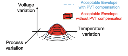
Figure 1: Acceptable envelope between with and without PVT detection [1]
In this investigation, high precision P, V, T, and L detectors are proposed, respectively. The proposed Voltage Variation Detector is featured with a delay line composed of high-Vth MOS-based delay cells. The proposed Temperature Detector consists of a temperature sensitive current generator, a Charge and Discharge Circuit (CDC), and a Voltage Window Comparator (VWC). Lastly, the proposed process variation detectors comprises separate NMOS and PMOS process variation detectors such that all the possible process corners will be detected. Measurement given that the proposed corner detectors are realized using 0.18 micro meter CMOS technology node show that the voltage detecting resolution is as good as 0.5% of VDD, and temperature detecting resolution is proved to be 3 ◦C in [-40 ◦C, +80 ◦C], and all the process variations, (SS, SF, TT, FS, FF), are detectable. Moreover, the leakage of PMOS and NMOS can be exactly detected by Leakage Detector, respectively.
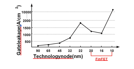
Figure 2: Gate leakage of different technology nodes [2], [3]
2. High-precision PVTL detector
Figure 3 shows the block diagram of the proposed on-chip highprecision PVTL detector contains the PMOS Variation Detector, NMOS Variation Detector, Temperature Detector, Voltage Variation Detector, and Leakage Detector. The details of each sub-circuit are given in the following text.
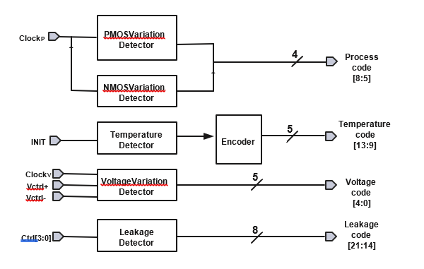
Figure 3: Proposed PVTL detecting system
2.1. Voltage Variation Detector
The schematic of Voltage Variation Detector in Figure 3 is shown in Figure 4, consisting of a buffer delay line (BF1-BF6), DFFs (FF1-FF6), XORs, and a Controllable delay block. Notably, all the cells in this circuit is also driven by the same input voltage (VDD). The operation of this circuit is summarized as follows:
- Due to the variation of input voltage (VDD), the delay generated by the buffer delay line will be varied accordingly.
- The generated codes at each delay cell are registered by corresponding DFFs, which are then the output of the adjacent DFF to generate Voltage code, V[0]-V[4].
- The last output of the buffer delay line, namely D6, is coupled to an input of Controllable delay block to form a feedback system.
Since Controllable delay block is meant to monitor the clock drift caused by voltage variation, the delay of each stage therein shall be auto-tuned by input voltage (VDD) and the final delay generated by the mentioned buffer delay line, e.g., D6. The schematic of the delay stage in Controllable delay block is revealed in Figure 5. It is notably featured with high Vth devices to prevent possible device parameter variation thanks to its thick gate oxide. D6 of buffer delay line is coupled to Vctrl+ and Vctrl- such that both the pull-up and pull-down switches have turned into a voltage controlled resistor.
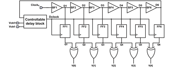
Figure 4: Schematic of the proposed Voltage Variation Detector
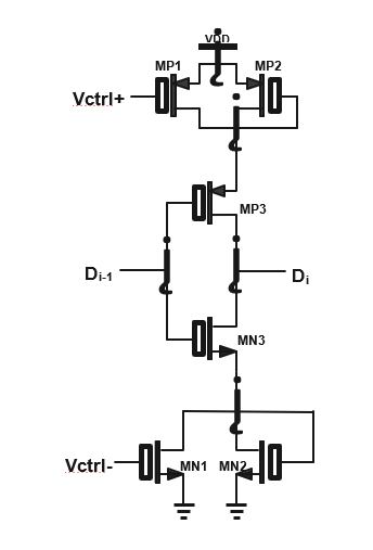
Figure 5: Schematic of the symmetric load delay cell
2.2. Process Variation Detector
The schematics of PMOS Variation Detector and NMOS Variation Detector in Figure 3 are shown in Figure 6 and Figure 7, respectively. Two individual process variation detectors are required for PMOS and NMOS to find out all the possible process corners. Take the N-type process variation detector in Figure 6 as an example. ClockP is coupled from the system clock source to an NAND gate to trigger the ring oscillator composed of only NMOS delay stages. As shown in Figure 7, different pulse counts (11, 6, 2) are attained at the counter output given that NMOS are at F (fast), T (typical), S (slow) corners respectively, when ClockP is high.
As for PMOS process variation detector, because the pulse count generated by PMOS devices in different corners is small, the threshold voltage is used to judge the changes in different process corners. When the ClockP drops to low, MP17 in Figure 6 will be turned on and discharged to Vth of the PMOS. Similarly, MP18 will be discharged to twice Vth of the PMOS. The comparator is compared with the two bias voltages (vbias1 and vbias2) to determine the corner which it is now.
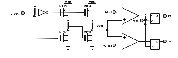
Figure 6: Schematic of the proposed PMOS Variation Detector
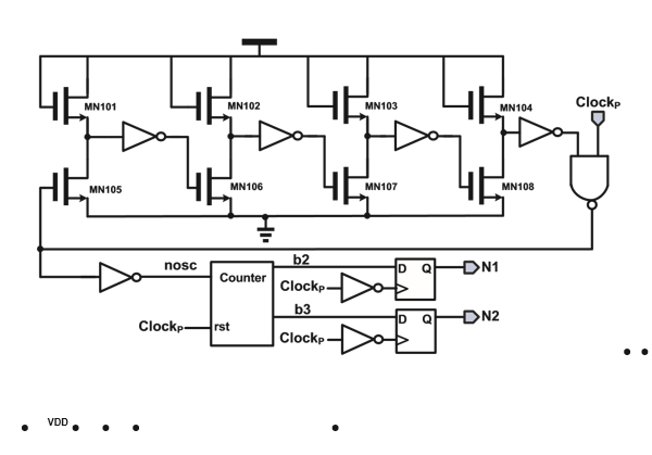
Figure 7: Schematic of the proposed NMOS Variation Detector
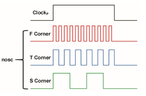
Figure 8: Waveforms of NMOS Variation Detector
2.3. Temperature Detector
The block diagram of Temperature Detector in Figure 3 is shown in Figure 9, consisting of a Current Generator (CG), a Charge and Discharge Circuit (CDC), a Voltage Window Comparator (VWC), and an Encoder. The schematic of CG, CDC, and VWC is given in Figure 10. Current Generator is charge of generating a current highly correlated to temperature variation. The operation of CDC and VWC is summarized as follows:
- Charging operation: The switch sw1 is shorted to node a1. Then, the storage capacitor, cap, starts to be charged via saturated MP12.
- Discharging operation: As soon as the voltage of the cap, Vcap(T), reaches VH, the output of VWC, VOUT(T), is switched low to short-circuit sw1 to node b1. MN13 is tuned on to be able to sink a current which is twice of the charging current provided by MP13. Thus, cap is discharged. As soon as the Vcap(T) is pulled down to VL, VOUT(T) will be turned high to start another cycle of charging-and-discharging operation.
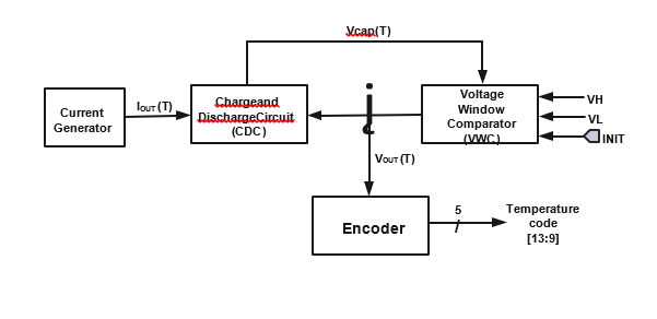
Figure 9: The block diagram of the proposed Temperature Detector
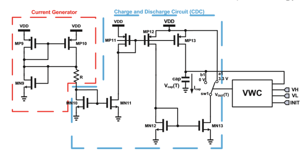
Figure 10: Schematic of the proposed Temperature Detector
Vcap(T) is compared with two pre-defined voltages, VH and VL, in VWC. If Vcap(T) ¿ VH, VOUT(T) = 0. On the contrary, if Vcap(T) ¡ VL, VOUT(T) = VDD. This result in the temperature is converted into a string of pulses, where higher temperature results in higher pulse count and vice versa. The frequency of the output FOUT(T)
= Icap(T)/2 · Ccap · (VH − VL). The relationship between FOUT(T) and temperature by simulation is shown in Figure. 11, which temperature would be detected correctly in every ◦C, and the maximum error is 0.59% at 37◦C.
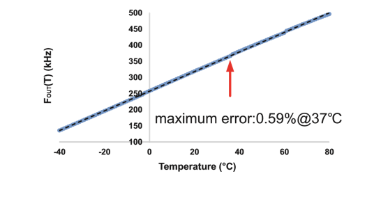
Figure 11: Theoretical function between FOUT(T) and temperature by simulation
2.4. Leakage Detector
The schematic of Leakage Detector in Figure 3 is shown in Figure
12, consisting of a Strobe pulse generator, a Switch, two PMOS Leakage detectors, two NMOS Leakage detectors, a Voltage-tofrequency converter (VFC), and a Counter.
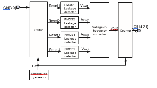
Figure 12: Schematic of the proposed Leakage Detector
The operation of the proposed Leakage Detector is summarized as follows:
- The Strobe pulse generator generates pulses which is the control signal of the four Leakage detectors and the Counter.
- Using the control signal Ctr and Ctrl[3:0] to select PMOS and NMOS with different aspect ratios as the object of leakage detection.
- The selected Leakage detector charges the capacitor with the leakage of a single PMOS or NMOS, and then converts the capacitor voltage output into a periodic square wave by the Voltage-to-frequency converter.
- The number of pulses of the periodic square wave is counted by Counter. If the larger the leakage is, the charging voltage of the capacitor will rise faster. Thus, the number of pulses registered in the counter will be higher.
Figure 13 shows the schematic of a PMOS Leakage detector and the equivalent voltage source model, which is the same as a DC transient circuit for RC charging and discharging. The function of NMOS Leakage detector is similar.
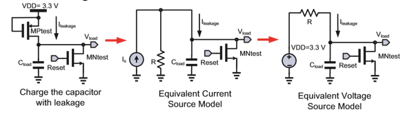
Figure 13: Equivalent model of Leakage Detector
Therefore, according to Eqn. (1) governed by Kirchhoff’s voltage law (KVL), the capacitor charging voltage Eqn. (2) and the capacitor charging current Eqn. (3) can be derived,
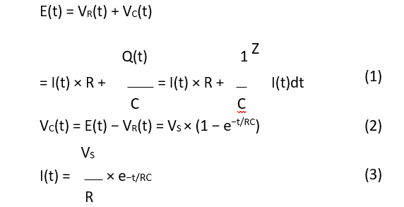
where VR(t) is the voltage across the resistor, VC(t) is the capacitor voltage, VS is the supply voltage (VDD), and e is the natural logarithm. When the circuit current drops from the maximum value to 36.8 %, the time is the product of the resistance and the capacitance, so the time constant (τ) of the RC charging circuit is the product of resistance and capacitance, as shown in Eqn. (4).

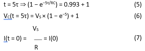
Through the natural logarithmic function calculation, as shown in Eqn. (5) and (6), the time for the capacitor charging to be stable is 5τ, and then the resistance R is derived. Thus, referring to Eqn. (3) to derive the capacitor charging current at any time. In addition, the charging current would decrease by time. The initial PMOS leakage charging current I(0) is as shown in Eqn. (7).
3. Measurement and Verification
This proposed PVTL detector design is realized using TSMC 180 nm CMOS process. The layout and die photo of the entire PVTL detector are shown in Figure 14 (a) and (b), respectively, where the core area is 1156×1671 µm2, and the total chip area is 2493×2553 µm2. The chip measurement setup of the proposed design is shown in Figure 15. The chip is soldered on the PCB to reduce noise interference. The Power Supply Agilent E3631A provides the required voltages to the chip. Arbitrary Waveform Generator Agilent 33522A and Signal Generator provide the ClockV and ClockP, respectively. The Programmable Compact Temperature & Humidity System is the equipment to define the environment temperature. The oscilloscope WaveRunner610Zi is used to observe waveforms and check the circuit operations.
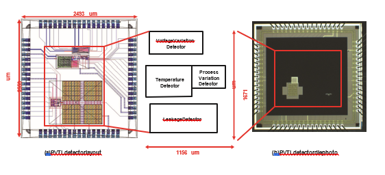
Figure 14: (a) PVTL detector layout; (b) PVTL detector die photo
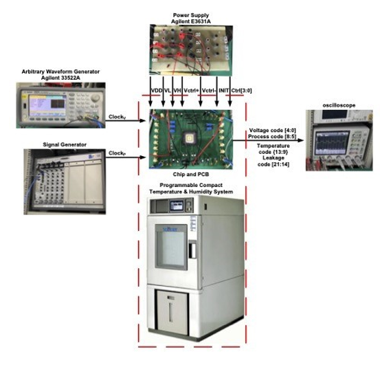
Figure 15: Measurement setup and equipment
A total of six chips are measured 10 times per chip to verify the reliability. The details of each measurement of sub-circuit are given in the following text.
3.1. Voltage Variation Detector
Figure 16 shows the measurement waveforms of the output signals of Voltage Variation Detector. It shows that Voltage code[4:0] is changed when VDD varies. The VDD is drifted by ±1%, ±0.5%, and 0%. Therefore, the measurement result proves the correctness of Voltage Variation Detector.
3.2. Process Variation Detector
Figure 17 shows the measurement waveforms of the output signals of Process Variation Detectors. It shows that the Process code is 0000 by all six chips. Thus, all PMOS and NMOS are made by SS corner. Notably, it is hard to ask foundry to deliberately fabricate the dies/chips at different process corners.
3.3. Temperature Detector
The interval between each measurement is at least an hour to ensure that the temperature of the entire chip and PCB is stable. Table 1 summarizes all the readings in the measurement, where the initial temperature is 20 ◦C, and the initial FOUT(T) is 206 kHz. By tuning Programmable Compact Temperature & Humidity System, the temperature and FOUT(T) rise continuously. In addition, FOUT(T) in measurement is lower than that given by the simulations due to the loading of the passive components and PCB. However, FOUT(T)-temperature curve is still linear in measurement. The error in Table 1 is calculated with the FOUT(T) by the linear regression.
The maximum error is 2.24 % at -5 ◦C, while the overage error is 0.773 %.
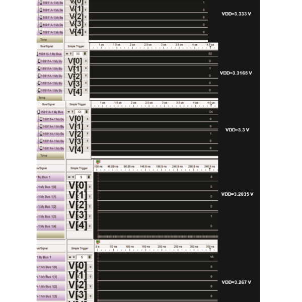
Figure 16: The measurement result of voltage variation
3.4. Leakage Detector
Referring to the analysis of the pulse count and leakage current which is shown in Figure 18 and the measurement waveforms of Leakage Detector shown in Figure 19. Figure 19 (a) and (b) are the PMOS Leakage Detector measurement outcome. The size of the PMOS under test in (a) is 50 µm/0.35 µm, and the pulse count is 31 equivalent to 31 pA. The size of the PMOS under test in (b) is 100 µm/0.35 µm, and the pulse count of (b) is 35 equivalent to 35 pA. Figure 19 (c) and (d) are the NMOS Leakage Detector measurement outcome. The size of the NMOS under test in (c) is 50 µm/0.35 µm, and the pulse count is 30 equivalent to 30 pA. The size of the NMOS under test in (d) is 100 µm/0.35 µm, and the pulse count is 55 equivalent to 55 pA. Therefore, the pulse count of the proposed Leakage Detector is positively correlated with the leakage of PMOS and NMOS.
|
Table 1: Measurement outcome of the proposed Temperature Detector
Table 2: Performance comparison of Output Buffers
|
|||||||||||||||||||||||||||||||||||||||||||||||||||||||||||||||||||||||||||||||||||||||||||||||||||||||||||||||||||||||||||||||||||||||||||||||||||||||
FOMa = Temperature RangeVDD Variation · Normalized Chip Area· PVT corner detected
FOMb = Temperature RangeVDD Variation· PVT corner detected
3.5. Performance comparison
Table 2 tabulates the performance comparison of several recent PVTL detector works. This work attain the best FOMb and the highest accuracy among all PVTL detector works in 2011-2020. However, due to the fact that four individual detectors are used, the proposed design pay the price of larger area. If the area is a factor be considered, FOMa, is also given and defined in Table 2. Apparently, it is a trade-off between high performance and large area.
4. Conclusion
A highly accurate on-chip PVTL detector design is demonstrated in this investigation, where four individual detectors are used to assist the quality improvement of chips implemented by CMOS. If the ICs’ leakage and PVT corner are correctly estimated, the host controller will be able to perform better.
5. Acknowledgment
This work was partially supported by FocalTech Systems Co., Ltd, Taiwan, under grant NO. N109130. The authors would like to express their deepest gratefulness to TSRI (Taiwan Semiconductor Research Institute), Taiwan, for their chip fabrication service.
- C.-C. Wang, W.-J. Lu, K.-W. Juan, W. Lin, H.-Y. Tseng, and C.-Y. Juan, ”Pro- cess corner detection by skew inverters for 500 MHz 2 VDD output buffer using 40-nm CMOS technology,” Microelectronics Journal, vol. 46, no. 1, pp. 1-11, Jan. 2015.
- H. F. Dadgour, S. Lin, and K. Banerjee, ”A statistical framework for estima- tion of full-chip leakage-power distribution under parameter variations,” IEEE Trans. on Electron Devices (TED), vol. 54, no. 11, pp. 2930-2945, Nov. 2007.
- Z. Abbas, A. Zahra, M. Olivieri, and A. Mastrandrea ”Geometry scaling impact on leakage currents in FinFET standard cells based on a logic-level leakage estimation technique,” Microelectronics, Electromagnetics and Telecommuni- cations, vol. 521, no. 4 pp.283-294, Jun. 2018.
- S.-K. Shin, W. Yu, Y.-H. Jun, J.-W. Kim, B.-S. Kong, and C.-G. Lee, ”Slew-rate- controlled output driver having constant transition time over process, voltage, temperature, and output load variations,” IEEE Trans. on Circuits and Systems II: Express Briefs (TCAS-II), vol. 54, no. 7, pp. 601-605, Jul. 2007.
- R.-C. Kuo, H.-Y. Tseng, J.-W. Liu, and C.-C. Wang, ”On-chip process and tem- perature compensation and self-adjusting slew rate control for output buffer,” in Proc. Asia Pacific Conf. on Postgraduate Research in Microelectronics Electronics (PrimeAsia), pp. 37-40, Oct. 2011.
- T.-J. Lee, W. Lin, and C.-C. Wang, ”Slew rate improved 2 VDD output buffer using leakage and delay compensation,” in Proc. IEEE Inter. Conf. on Electron Devices and Solid-State Circuits (EDSSC), pp. 1-2, Jun. 2014.
- C.-L. Chen, H.-Y. Tseng, R.-C. Kuo, and C.-C. Wang, ”On-chip MOS PVT variation monitor for slew rate self-adjusting 2 VDD output buffers,” in Proc. IEEE Inter. Conf. on IC Design Technology (ICICDT), pp. 1-4, May 2012.
- C.-L. Chen, H.-Y. Tseng, R.-C. Kuo, and C.-C. Wang, ”A slew rate self- adjusting 2 VDD output buffer with PVT compensation,” in Proc. IEEE VLSI Design, Automation and Test (VLSI-DAT), pp. 1-4, Apr. 2012.
- C.-C. Wang, C.-L. Chen, R.-C. Kuo, H.-Y. Tseng, J.-W. Liu, C.-Y. Juan, ”On- chip process and temperature monitor for self-adjusting slew rate control of 2 VDD output buffers,” IEEE Trans. on Circuits and Systems I: Regular Papers (TCAS-I), vol. 60, no. 6, pp. 1432-1440, Jun. 2013.
- T.-J. Lee, K.-W. Ruan, and C.-C. Wang, ”32% slew rate and 27% data rate improved 2 VDD output buffer using PVTL compensation,” in Proc. IEEE
echnology (ICICDT), pp. 1-4, May 2014. - C.-C. Wang, T.-Y. Tsai, T.-J. Lee, and K.-W. Ruan, ”2 VDD output buffer with 36.4% slew rate improvement using leakage current compensation,” Electronics Letters (EL), vol. 53, no. 2, pp. 62-64, Jan. 2017.
- C.-C. Wang, T.-Y. Tsai, and W. Lin, ”A 90-nm CMOS 800 MHz 2 VDD out- put buffer with leakage detection and output current self-adjustment,” Analog Integrated Circuits and Signal Processing (AICSP), vol. 97, no. 2, pp. 343-350, Nov. 2018.
- S. A. Tawfik, and V. Kursun, ”Multi-Vth level conversion circuits for multi- VDD systems,” in Proc. Inter. Symp. on Circuits and Systems (ISCAS), pp. 1397-1400, May 2007.
- W.-P. Tu, S.-W. Wu, S.-H. Huang, and M.-C. Chi, ”NBTI-aware dual threshold voltage assignment for leakage power reduction,” in Proc. Inter. Symp. on Circuits and Systems (ISCAS), pp. 349-352, May 2012.
- M. Liu, W.-S. Wang, and M. Orshansky, ”Leakage power reduction by dual-Vth designs under probabilistic analysis of Vth variation,” in Proc. Inter. Symp. on Low Power Electronics and Design (ISLPED), pp. 2-7, Aug. 2004.
- T. Shirai, and K. Usami, ”Hybrid design of dual Vth and power gating to reduce leakage power under Vth variations,” in Proc. Inter. SoC Design Conf. (ISOCC), pp. 310-313, Nov. 2008.
- C. S. Nagarajan, L. Yuan, G. Qu, and B. G. Stamps, ”Leakage optimization using transistor-level dual threshold voltage cell library,” in Proc. Inter. Symp. esign (ISQED), pp. 62-67, Mar. 2009.
- M.-D. Ker, and P.-Y. Chiu, ”Design of 2 VDD-tolerant I/O buffer with PVT compensation realized by only 1 VDD thin-oxide devices,” IEEE Trans. on Circuits and Systems I: Regular Papers (TCAS-I), vol. 60, no. 10, pp. 2549- 2560, Oct. 2013.
- Y.-H. Kwak, I. Jung, and C. Kim, ”A Gb/s+ slew-rate/impedance-controlled output driver with single-cycle compensation time,” IEEE Trans. on Circuits and Systems II: Express Briefs (TCAS-II), vol. 57, no. 2, pp. 120-125, Feb. 2010.
- T.-J. Lee, T.-Y. Tsai, W. Lin, U.-F. Chio, and C.-C. Wang, ”A slew rate varia- tion compensated 2 VDD I/O buffer using deterministic P/N-PVT variation detection method,” IEEE Trans. on Circuits and Systems II: Express Briefs (TCAS-II), vol. 66, no. 1, pp. 116-120, Jan. 2019.
- T.-J. Lee, T.-Y. Tsai, W. Lin, U.-F. Chio, and C.-C. Wang, ”A dynamic leakage and slew rate compensation circuit for 40-nm CMOS mixed-voltage output buffer,” IEEE Trans. on Very Large Scale Integration (VLSI) Systems (TVLSI), vol. 25, no. 11, pp. 3166-3174, Nov. 2017.
- T.-Y. Tsai, Y.-Y. Chou, and C.-C. Wang, ”A method of leakage reduction and slew-rate adjustment in 2 VDD output buffer for 28 nm CMOS technology and above,” in Proc. Inter. Conf. on IC Design and Technology (ICICDT), pp. n. 2016.