
Hole-Confined Polar Optical Phonon Interaction in Al0.35Ga0.65As/GaAs/Al0.25Ga0.75As Quantum Wells
Volume 7, Issue 3, Page No 82-86, 2022
Author’s Name: Mohamed Boumaza1,a), Yacine Boumaza2
View Affiliations
1Teacher Education college of Setif Messaoud Zeghar, Department of sciences, El Eulma, 19600, Algeria
2Batna 1 University, Department of Electrical Engineering, Faculty of Technology, 05000 DZ, Algeria
a)whom correspondence should be addressed. E-mail: mboumazaphy1@gmail.com
Adv. Sci. Technol. Eng. Syst. J. 7(3), 82-86 (2022); ![]() DOI: 10.25046/aj070309
DOI: 10.25046/aj070309
Keywords: Quantum Well, Confined Phonon, Semiconductor

Export Citations
In Al0.35Ga0.65As/GaAs/Al0.25Ga0.75As quantum wells, the hole-confined polar optical phonon interaction is investigated. To calculate the valence band structure, we use the Luttinger-Kohn Hamiltonian with the k.p method. Within the dielectric continuum model, the hole-confined phonon scattering rates of intrasubband heavy holes in quantum well are calculated. It is found that the scattering rates are governed by an overlap integral and the density of states. Moreover, the scattering rates are reduced under compressive hydrostatic strain for low hole energy. The anisotropic effect on hole-confined phonon interaction is also studied.
Received: 19 March 2022, Accepted: 15 May 2022, Published Online: 25 May 2022
1. Introduction
In physics, electron-phonon interaction plays an important role such as spin relaxation [1], superconductivity [2], quantum laser [3], mobility [4], Carrier thermalization [5]. Over the past decade, there has been an increasing interest of GaAs/AlxGa1-xAs heterostructures with a variety of structures such as heterojunction [6], quantum well [7], quantum wire [8], quantum dot [9], multiquantum well [10], superlattice [11]. It is well known that phonons are confined in quantum well which has proven experimentally [12–14]. Furthermore, to describe the optical phonons in quantum well there are several models such as the dielectric continuum model (DCM) in [15], the hydrodynamic model in [16], the microscopic model in [17], and the hybrid model of in [18]. In the case of other structures such as periodic soliton we use the new generalized -expansion method [19].
In this paper, we calculate the valence band structure using the 6×6 Luttinger-Kohn Hamiltonian, taking into account the warping in Al0.35Ga0.65As/GaAs/Al0.25Ga0.75As asymmetric quantum well [20,21] within the k.p method due to its simplicity and accuracy [22], whereas to describe the phonons in the quantum well, we use the dielectric continuum model which has been used by several authors [23–27], and given excellent results compared to the experimental results [28, 29]. In addition, we investigate hole confined phonon scattering rates for different quantum well widths and the results are discussed. We also study the scattering rates under compressive hydrostatic strain using the theory of Luttinger–Kohn and Bir–Pikus [30].
2. Theory
In our work, we consider an asymmetric quantum well grown along the z direction. The 6×6 Luttinger Hamiltonian is transformed into two 3×3 matrixes [31,32], we calculate the hole band structure, by solving the Schrödinger equation including the heavy hole (HH), light hole (LH), and spin–orbit split-off subbands.
With the dielectric continuum model, the Frohlich Hamiltonian is written as [25]
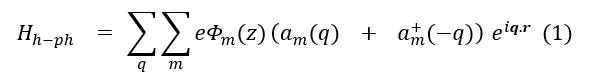
here is the phonon creation operator, is the phonon annihilation operator, is the normalized phonon potential, r is the position vector in the xy plane, m denotes the LO mode order index and q is the in-plane phonon wave vector.
Using the Fermi’s golden rule, the hole-confined phonon scattering rates from the initial hole state with the wave vector ki within subband i to the final hole states in subband f with wave vector kf are calculated as [33]
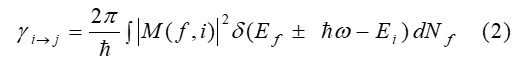
here, Nf is the number of final states, Ei is the initial hole state energie, Ef is the final hole state energie, M ( f , i ) is the function connecting between the initial and the final hole states. Equation (2) yields
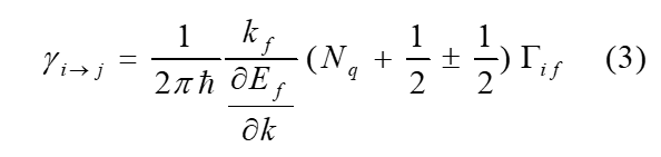
where Nq is the phonon occupation number, is the function of the hole wave function and the phonon potential, which is written as
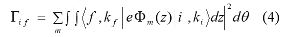
In Equation (4) the integration is done numerically where momentum and energy are conserved. The phonon potential is provided by [25]
here L is quantum well width, AC is the normalization constant [25].
3. Results and discussions
In our work, we use the material parameters listed in Table [34–36]
Table 1: Parameters used in our work
| Parameter | Unit | GaAs | AlAs |
| 6.85 | 3.69 | ||
| 2.1 | 0.79 | ||
| 2.9 | 1.4 | ||
| eV | 0.341 | 0.28 | |
| eV | 1.424 | 2.671 | |
| eV | -1.16 | -2.47 | |
| eV | 0.03625 | 0.05009 |
Figure 1 shows the valence band structure of a 25 Å Al0.35Ga0.65As/GaAs/Al0.25Ga0.75As asymmetric quantum well in the kx – ky plane showing a great nonparabolicity with lifted spin degeneracy. Because of the coupling between the heavy hole and light hole subbands, our results exhibit a strong anisotropy along the [10] and [11] directions. We note here that the heavy hole subband is more anisotropic than the light hole subband in particular for high energies.
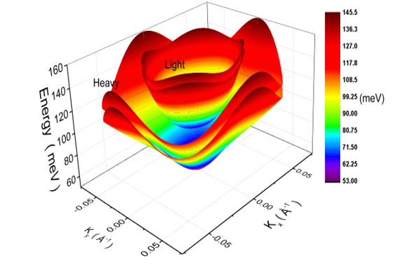
Figure 1: Heavy hole subband and light hole subband structures as a function of wave vector k in the kx – ky plane for L = 25 Å and for clarity, the split off subband is not shown.
Figure 2.a shows the intrasubband heavy holes scattering rates of the confined optical phonon absorption as function of initial hole energy for different well widths, whereas the function Гi f is shown in (b).
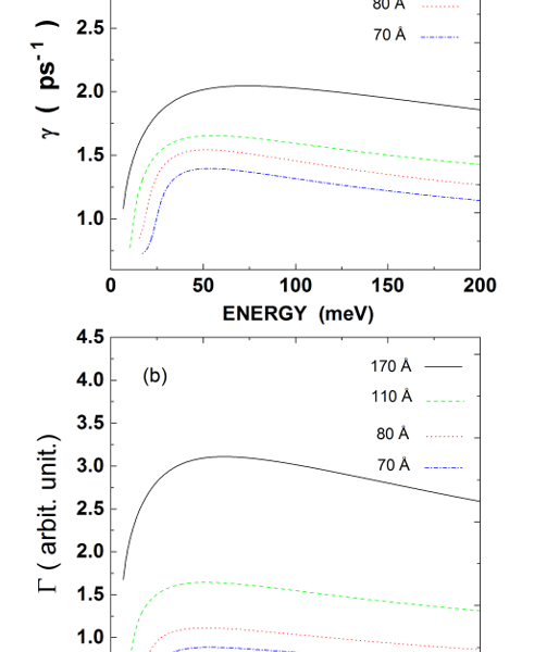
Figure 2 : a) Intrasubband scattering rates of heavy hole for different well widths respectively 70 Å, 80 Å , 110 Å, 170 Å b) The function
The scattering rates depend on the density of states and the function Гi f. Therefore, to understand our results, we plot in Figure 3 the dependence of the density of states on the hole energies.
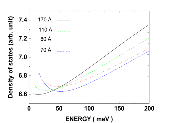
Figure 3: Density of states D(E) of heavy hole as function of hole energy and for different well widths.
One can see that for low hole energy scattering rates increase rapidly with increasing hole energy to reach its maximum value. However, for high hole energies although the density of states increases with increasing hole energy, scattering rates show a very slight decrease. This indicates that the scattering rate shows only a weak dependence on the density of states. The maximum value of the scattering rate is 1.39×10¹² s-1 for L = 70 Å while the scattering rate reaches its highest value 2.045 x10¹² s-1 for L = 170 Å
It is well known that under hydrostatic strain valence band structure is altered, which leads to a significant change in the scattering rate. In order to study the scattering rates under strain, we show in figure 4 a) Heavy hole scattering rates for the confined optical phonon absorption as function of the initial hole energy for two quantum well widths 70 Å and 170 Å b) The overlap integral Гi f. The dashed lines depict the scattering rates for 2 % of compressive hydrostatic pressure, whereas the solid lines for the results in the absence of strain. For low hole energy and for quantum well width L = 70 Å ( L = 170 Å ) scattering rates under strain are reduced by about 46.5 % ( 64 % ), on the other hand, for high hole energy and for L = 70 Å ( L = 170 Å ) scattering rates are increased by about 2.8 % ( 2.3 % ). This behavior is similar to the function Гi f.
Figure 5 shows the scattering rate for the confined optical phonon as a function of the initial two dimensional wave vector k with including the warping in the valence subband structure. For clarity, we also plot in Figure 6 and 7 the scattering rates for confined phonon absorption as a function of the initial hole wave vector k in polar coordinates for two well widths L = 25 Å and L = 170 Å respectively. One can see that for the quantum well width L = 25 Å our results exhibit significant anisotropic behavior for high hole energies between the directions [0 1] and [1 1], in which scattering rates increase by 14.7 %. However, for the quantum well width L = 170 Å scattering rates decrease by 54.5 %. This anisotropy is due to the strong valence subband anisotropy.
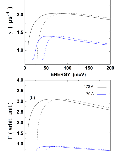
Figure 4: a Scattering rates within heavy hole subband for the confined optical phonon absorption and for two different well widths 70 Å and 170 Å b) The overlap integral Гi f. The solid lines and dashed lines stand for the results without a strain with 2 % compressive hydrostatic pressure respectively.
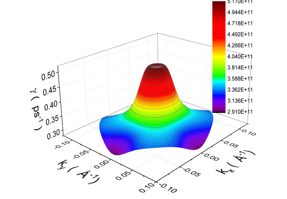
Figure 5: Scattering rates within heavy hole subband for confined optical phonon absorption with including warping as a function of the initial hole wave vector k in the kx-ky plane and for L = 25 Å
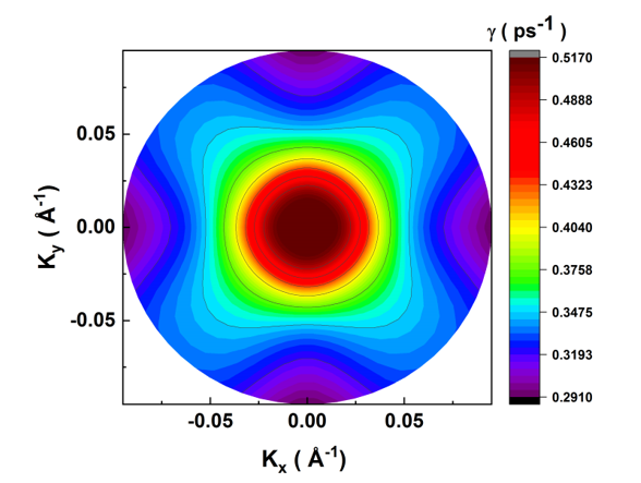
Figure 6: Scattering rates within heavy hole subband for confined optical phonon absorption as a function of the initial hole wave vector k in polar coordinates and for L = 25 Å
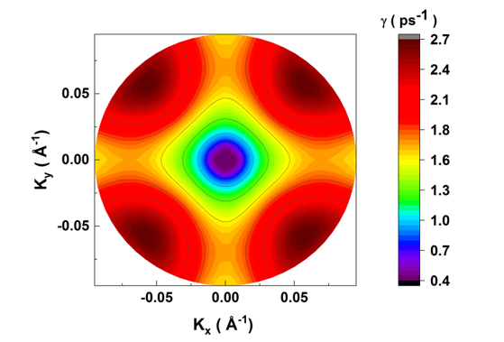
Figure 7: Scattering rates within heavy hole subband for confined optical phonon absorption as a function of the initial hole wave vector k in polar coordinates and for L = 170 Å
4. Conclusion
In summary, with the k.p method, the valence band structure is calculated including spin-orbit split-off subbands effect in the Al0.35Ga0.65As/GaAs/Al0.25Ga0.75As asymmetric quantum wells. Hole-confined polar optical phonon scattering rates are investigated using the dielectric continuum model. It is found that scattering rates increase with increasing quantum well width. Moreover, under compressive hydrostatic strain, the scattering rates are reduced, in particular for low hole energy. In addition, scattering rates follow mostly the behavior of the overlap integral and exhibit a strong anisotropy for high hole energy. This anisotropy increases with increasing quantum well width. Our results show the importance of the band structure engineering quantum well via strain and within the asymmetric quantum well to reduce scattering rates and, consequently, the mobility of carriers can be increased. In the future, we will extend our work to different quantum well growth directions.
Conflict of Interest
The authors declare no conflict of interest.
- J. Park, J.-J. Zhou, M. Bernardi, “Spin-phonon relaxation times in centrosymmetric materials from first principles,” Physical Review B, 101(4), 045202, 2020, doi:10.1103/PhysRevB.101.045202.
- M. Li, Y. Fang, C. Kenney-Benson, L. Wang, “Superconductivity and electron–phonon interaction in SrxBi2Se3 under pressure,” New Journal of Physics, 23(8), 083011, 2021, doi:10.1088/1367-2630/ac14cf.
- A. Demić, Z. Ikonić, P. Dean, D. Indjin, “Dual resonance phonon–photon–phonon terahertz quantum-cascade laser: physics of the electron transport and temperature performance optimization,” Optics Express, 28(26), 38788–38812, 2020, doi:10.1364/OE.410014.
- T. Nematiaram, D. Padula, A. Landi, A. Troisi, “On the Largest Possible Mobility of Molecular Semiconductors and How to Achieve It,” Advanced Functional Materials, 30(30), 2001906, 2020, doi:10.1002/adfm.202001906.
- A. Asgari, L. Faraone, “Thermal broadening of electron mobility distribution in AlGaN/AlN/GaN heterostructures,” Journal of Applied Physics, 114(5), 053702, 2013, doi:10.1063/1.4813866.
- A. Sužiedėlis, S. Ašmontas, J. Gradauskas, V. Nargelienė, A. Čerškus, A. Lučun, T. Anbinderis, I. Papsujeva, A. Narkūnas, B. Kundrotas, R. Rinkevičienė, “Peculiarities of Temperature Dependence of Detected Voltage by GaAs/Al0.25Ga0.75As Heterojunction Microwave Diode Near Interwalley Crossover,” Materials Science, 20(2), 138–140, 2014, doi:10.5755/j01.ms.20.2.6319.
- T. Kawazu, “Valence Band Mixing in GaAs/AlGaAs Quantum Wells Adjacent to Self-Assembled InAlAs Antidots,” Journal of Nanomaterials, 2019, e5349291, 2019, doi:10.1155/2019/5349291.
- K.D. Pham, C.V. Nguyen, N.N. Hieu, H.V. Phuc, B.D. Hoi, B.M.H. Hoa, L.T.T. Phuong, “Theoretical investigation of hot electron cooling process in GaAs/AlAs cylindrical quantum wire under the influence of an intense electromagnetic wave,” Optical and Quantum Electronics, 50(9), 342, 2018, doi:10.1007/s11082-018-1606-x.
- S. Germanis, P. Atkinson, R. Hostein, S. Suffit, F. Margaillan, V. Voliotis, B. Eble, “Electrical control of optically pumped electron spin in a single GaAs/AlAs quantum dot fabricated by nanohole infilling,” Physical Review B, 102(3), 035406, 2020, doi:10.1103/PhysRevB.102.035406.
- O. Kojima, T. Kita, M.J. Steer, R.A. Hogg, “Modulation of exciton states through resonant excitation by continuous wave lasers in a GaAs/AlAs multiple quantum well,” Journal of Physics D: Applied Physics, 54(33), 2021.
- H. Eisele, L. Li, E.H. Linfield, “High-performance GaAs/AlAs superlattice electronic devices in oscillators at frequencies 100–320 GHz,” Applied Physics Letters, 112(17), 172103, 2018, doi:10.1063/1.5020265.
- A.K. Sood, J. Menéndez, M. Cardona, K. Ploog, “Interface Vibrational Modes in GaAs-AlAs Superlattices,” Physical Review Letters, 54(19), 2115–2118, 1985, doi:10.1103/PhysRevLett.54.2115.
- M.V. Klein, “Phonons in semiconductor superlattices,” IEEE Journal of Quantum Electronics, 22(9), 1760–1770, 1986, doi:10.1109/JQE.1986.1073174.
- A.K. Sood, J. Menéndez, M. Cardona, K. Ploog, “Resonance Raman Scattering by Confined LO and TO Phonons in GaAs-AlAs Superlattices,” Physical Review Letters, 54(19), 2111–2114, 1985, doi:10.1103/PhysRevLett.54.2111.
- R. Fuchs, K.L. Kliewer, “Optical Modes of Vibration in an Ionic Crystal Slab,” Physical Review, 140(6A), A2076–A2088, 1965, doi:10.1103/PhysRev.140.A2076.
- M. Babiker, “Longitudinal polar optical modes in semiconductor quantum wells,” Journal of Physics C: Solid State Physics, 19(5), 683–697, 1986, doi:10.1088/0022-3719/19/5/008.
- K. Huang, B. Zhu, “Dielectric continuum model and Frohlich interaction in superlattices,” Physical Review B, 38(18), 13377–13386, 1988, doi:10.1103/PhysRevB.38.13377.
- B.K. Ridley, “Electron-hybridon interaction in a quantum well,” Physical Review B, 47(8), 4592–4602, 1993, doi:10.1103/PhysRevB.47.4592.
- Md.K. Alam, Md.D. Hossain, M.A. Akbar, K.A. Gepreel, “Determination of the rich structural wave dynamic solutions to the Caudrey–Dodd–Gibbon equation and the Lax equation,” Letters in Mathematical Physics, 111(4), 103, 2021, doi:10.1007/s11005-021-01443-9.
- P.C. Klipstein, Y. Livneh, O. Klin, S. Grossman, N. Snapi, A. Glozman, E. Weiss, “A k·p model of InAs/GaSb type II superlattice infrared detectors,” Infrared Physics & Technology, 59, 53–59, 2013, doi:10.1016/j.infrared.2012.12.009.
- S. Rodrı́guez, J.A. López-Villanueva, I. Melchor, J.E. Carceller, “Hole confinement and energy subbands in a silicon inversion layer using the effective mass theory,” Journal of Applied Physics, 86(1), 438–444, 1999, doi:10.1063/1.370749.
- Z. Becer, A. Bennecer, N. Sengouga, “Modeling Energy Bands in Type II Superlattices,” Crystals, 9(12), 629, 2019, doi:10.3390/cryst9120629.
- M. Boumaza, S. Lamari, “Anisotropic intrasubband hole scattering by polar optical phonon modes in thin GaAs/AlxGa1−xAs quantum wells,” Superlattices and Microstructures, 72, 156–163, 2014, doi:10.1016/j.spmi.2014.03.049.
- W.-D. Huang, G.-D. Chen, Y.-J. Ren, “Effect of ternary mixed crystals on interface optical phonons in wurtizte InxGa1−xN/GaN quantum wells,” Journal of Applied Physics, 112(5), 053704, 2012, doi:10.1063/1.4748173.
- N. Mori, T. Ando, “Electron–optical-phonon interaction in single and double heterostructures,” Physical Review B, 40(9), 6175–6188, 1989, doi:10.1103/PhysRevB.40.6175.
- J. Požela, K. Požela, V. Jucienė, “Scattering of electrons by confined interface polar optical phonons in a double-barrier heterostructure,” Semiconductors, 41(9), 1074–1079, 2007, doi:10.1134/S1063782607090126.
- A.M. Alcalde, G. Weber, “Scattering rates due to electron-phonon interaction in CdS1-xSex quantum dots,” Semiconductor Science and Technology, 15(11), 1082–1086, 2000, doi:10.1088/0268-1242/15/11/312.
- X. Zianni, C.D. Simserides, G.P. Triberis, “Electron scattering by optical phonons in AlxGa1−xAs/GaAs/AlxGa1−xAs quantum wells,” Physical Review B, 55(24), 16324–16330, 1997, doi:10.1103/PhysRevB.55.16324.
- V.V. Bondarenko, V.V. Zabudskii, F.F. Sizov, “Electron-phonon interaction and electron mobility in quantum-well type-II PbTe/PbS structures,” Semiconductors, 32(6), 665–667, 1998, doi:10.1134/1.1187461.
- Y. Kajikawa, “Optical anisotropy of (11l)-oriented strained quantum-wells calculated with the effect of the spin-orbit split-off band,” Journal of Applied Physics, 86(10), 5663–5677, 1999, doi:10.1063/1.371577.
- D.A. Broido, L.J. Sham, “Effective masses of holes at GaAs-AlGaAs heterojunctions,” Physical Review B, 31(2), 888–892, 1985, doi:10.1103/PhysRevB.31.888.
- C.Y.-P. Chao, S.L. Chuang, “Spin-orbit-coupling effects on the valence-band structure of strained semiconductor quantum wells,” Physical Review B, 46(7), 4110–4122, 1992, doi:10.1103/PhysRevB.46.4110.
- B.K. Ridley, Electrons and Phonons in Semiconductor Multilayers, 2nd ed., Cambridge University Press, Cambridge, 2009, doi:10.1017/CBO9780511581496.
- S. Boyer-Richard, F. Raouafi, A. Bondi, L. Pédesseau, C. Katan, J.-M. Jancu, J. Even, “30-band k⋅p method for quantum semiconductor heterostructures,” Applied Physics Letters, 98(25), 251913, 2011, doi:10.1063/1.3600643.
- I. Vurgaftman, J.R. Meyer, L.R. Ram-Mohan, “Band parameters for III–V compound semiconductors and their alloys,” Journal of Applied Physics, 89(11), 5815–5875, 2001, doi:10.1063/1.1368156.
- GaAs, AlAs, and AlxGa1−xAs: Material parameters for use in research and device applications: Journal of Applied Physics: 58(3), Mar. 2022.