Synthesis and Characterization of CN Thin Films Produced by DC-Pulsed Sputtering in an CH3CH2OH-N2 Atmosphere
Volume 7, Issue 1, Page No 53-59, 2022
Author’s Name: Marcos Crescencio González Domínguez1,a), Pedro Guillermo Reyes Romero1, Aarón Gómez Díaz1, Horacio Martínez Valencia2, Víctor Hugo Castrejón Sanchez3
View Affiliations
1Universidad Autónoma del Estado de México, Laboratorio de Física Avanzada, Facultad de Ciencias, Toluca, 50000, México
2Universidad Nacional Autónoma de México, Laboratorio de Espectroscopía, Instituto de Ciencias Fisicas, Cuernavaca, 48, México
3Tecnologico de Estudios Superiores de Jocotitlán, Jocotitlán, México
a)whom correspondence should be addressed. E-mail: kenny.sxe4@gmail.com
Adv. Sci. Technol. Eng. Syst. J. 7(1), 53-59 (2022); ![]() DOI: 10.25046/aj070106
DOI: 10.25046/aj070106
Keywords: CNx, Sputtering, Raman, SEM, AFM, OES

Export Citations
This paper reports on the successful deposition of amorphous carbon nitride thin films (a-CNx). Samples were deposited using a DC-pulsed sputtering technique in CH3CH2OH-N2 atmosphere at constant pressure (1 Torr). Raman spectra were collected to investigate the bonding structure of the deposed thin films, while scanning electron microscopy (SEM) and atomic force microscopy (AFM) were used to study thin-film surface morphology. Plasma characterization was performed during the deposition process using optical emission spectroscopy (OES), and the influence of the deposition process parameters on the chemical fragmentation of species present in the plasma was determined. Raman results were typical for a-CNx films, and SEM analysis showed that carbon clusters deposited onto the Cu substrate form a non-homogeneous surface. The morphology observed by AFM indicated that the thin films grow as islands, which corroborate the generation of amorphous structures grown on the Cu surface. OES spectra verified the existence of CN radicals within the CH3CH2OH/N2 plasma during thin-film deposition.
Received: 30 November 2021, Accepted: 31 January 2021, Published Online: 10 February 2022
1. Introduction
The miniaturization demands in the electronic industry required development of new materials that allow the creation of these miniature devices. A good candidate material is carbon, which has a wide variety of allotropic forms with interesting physical and chemical properties. Although the properties of diamond and graphite have been extensively investigated, there are other allotropic forms (fullerenes) that are of great interest today. Since its discovery, carbon nitride (CN) has aroused great interest in theoretical [1] and experimental studies, given its physical and chemical properties. Carbon nitrides have attracted attention owing to their potential applications in anti-corrosion photo-electrochemical technology [2], photo-degradation [3], and photo-catalysis [4, 5], which can be used in optoelectronics [6] and the manufacture of biosensors [7, 8]. From an experimental point of view, the most important material successes have been in the synthesis of carbon nitrides in the form of thin films by chemical and physical deposition of vapor. Among the physical deposition methods, the use of plasmas [9], especially the sputtering method [10], has been successfully implemented for deposition of carbon nitrides. Recently, a hybrid coating process that combines RF and DC sputtering systems has been successfully used: DC magnetron or DC-pulsed discharge [11, 12]. The advantages of these hybrid coating processes are that the various deposition parameters (e.g., working pressure, sputtering power, current, substrate bias voltage, and target material) can be adjusted separately to produce films with excellent mechanical and tribological properties.
The physical properties of carbon-based films depend upon different forms of hybrid bonds of the carbon atom: sp1, sp2, and sp3. The incorporation of nitrogen into the system enables the formation of different kinds of carbon configurations, including sp3 (tetrahedral bond), sp2 (triple bond) and C=N and N=C-type chains. These configurations improve the mechanical and physical properties of CNx compounds, increasing the application range of the films [13]. To the best of our knowledge, there are no publications in the literature reporting attempts to synthesize C-N compounds by CH3CH2OH-N2 DC-pulsed sputtering. Even more significantly, there still exist various unanswered queries about how the growth process impacts the resulting structure in amorphous CN (a-CNx) films. The purpose of this article is to investigate the morphological and microstructural properties of a-CNx films deposited by DC-pulsed sputtering in a CH3CH2OH-N2 plasma mixture. Characterization of the bond structure of the thin films was performed by Raman spectroscopy, and their morphology and microstructure were investigated using scanning electron microscopy (SEM) and atomic force microscopy (AFM). Plasma characterization during thin-film deposition was also carried out using optical emission spectroscopy (OES), and these findings are correlated to variations in microstructure and morphology of the thin films.
2. Materials and Method
Reactive sputtering is a suitable coating technique for the preparation of thin films. The pulsed DC sputtering deposition system used in this work (Figure 1) consists of a cylindrical stainless-steel chamber (33-cm long, 20-cm radius, and a volume of 1.04 × 103 cm3) and two mobile Cu electrodes (5-cm in diameters) placed in the center of the vacuum chamber with a separation space of 20 mm. The power supply consisted of Pinnacle Plus+ generators, which delivered DC power in a pulsing configuration to enable reactive sputtering. Pirani pressure sensors (MKS, model 103170027SH) were used to determine the total pressure in the chamber, and a flowmeter (Matheson Tri. Gas FM-1050) was used to regulate the gas flow within the system. An ocean optics spectrometer monitored the optical emission spectra generated within the discharge and the chamber vacuum was formed using a mechanical pump (Varian DS302). The background and working pressure of the vacuum chamber were 2 × 10⁻² and 1 Torr, respectively.
High-purity CH3CH2OH (99.9%) was used as the carbon precursor, and high-purity nitrogen (99.9%) was used both as the sputtering ion source, which bombards the target, and as the nitrogen species, which is introduced into the thin films with carbon ions. The relation of the mixture was 20%-CH3CH2OH to 80%-N2. To generate plasma, the vacuum chamber is first evacuated with a mechanical pump until a base pressure of 2 × 10⁻² Torr is reached; next, it is filled with CH3CH2OH-N2 mixture gas and discharge is generated by applying a pulsed current (300 mA at 450 V) between two electrodes. Then, the CH3CH2OH-N2 mixture gas is ionized and accelerated by the electrical field produced by the electrodes, forming an energetic ion beam that provides both sputtering ions and reacting nitrogen and carbon precursors. A Cu disk was used as a substrate for the growth of CNx films. Pulsed discharge was performed for 1 hour. The intention of growing CNx films on the surface of Cu
The bond structure and microstructure of the thin films was investigated using Raman spectroscopy (micro-Raman, LabRam HR 800 system). Raman measurements were recorded using a He–Ne laser, which was focused using a 50X lens. During the measurements, 60 recoded data were collected every 60 s. SEM (Jeol IT-100 coupled to a Bruker X-Ray microscope) and AFM (EasyScan 2 Flex AFM) were used to determine the thin-film morphology. The SEM microscope was operated in high voltage mode with an accelerating voltage of 20 kV. SEM studies were carried out on the electrolytic Cu (99.99%) substrate to observe the formation of attached carbon structures and thus corroborate their existence.
To characterize the plasma during film deposition, the species generated within the plasma discharge was observed by optical emission spectroscopy (OES). An ocean optics HR 4000CG-UV-NIR spectrometer was used, and spectra were observed in a wavelength range of 200 to 850 nm, with a resolution of 0.75-nm FWHM.
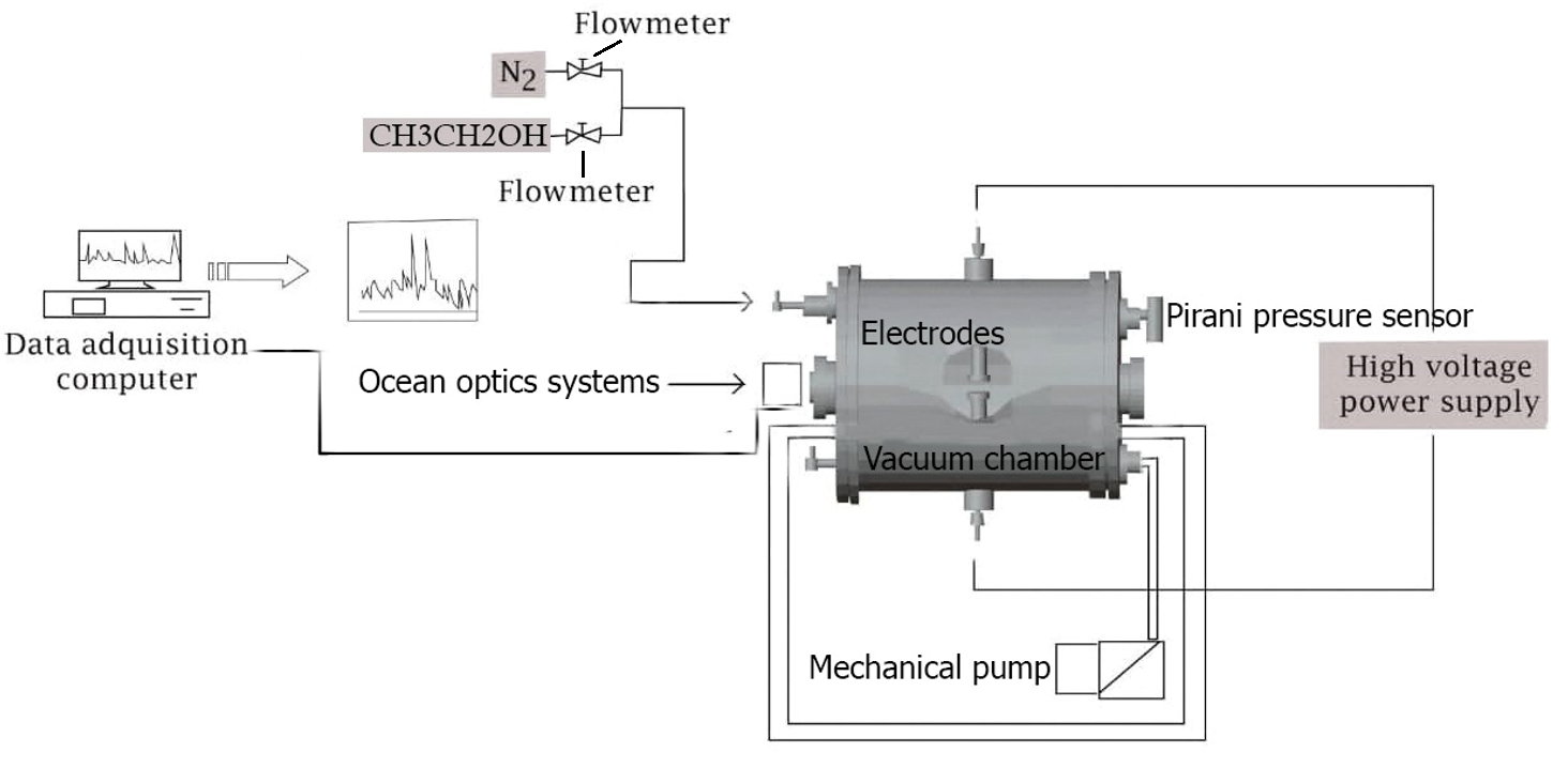 Figure 1: Experimental apparatus
3. Results and Discussion
3.1. Raman spectroscopy
Raman spectroscopy is commonly used to analyze the bond structure of carbon-related materials. Visible Raman spectroscopy is 50 to 230 times more sensitive to sp2 sites because p electrons are preferentially excited with visible photons [12]. Thus, the Raman spectra obtained for the deposited CNx films provided double-link information, in addition to indication of changes in film microstructure.
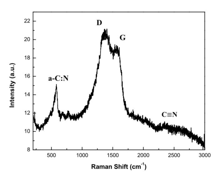 Figure 2: Raman spectra of thin CNx deposited by pulsed discharge at a pressure of 1 Torr.
Figure 2 shows Raman spectra for CNx films deposited onto Cu at 300 mA, 550 V and 120 W at a working pressure of 1 Torr. Raman bands appear at 692, 1,362 (D peak), 1,588 (G peak), and 2,250 cm−1 [14]. The 692 cm−1 band is characteristic of CN films deposited under the influence of a reactive gas. This band may also appear owing to structural disorder in the film. The G peak arises from stretching vibrations at all sp2 sites, both in olefinic chains and in aromatic rings, while the existence of the D peak is associated with breathing vibrations in the aromatic rings. These peaks, therefore, indicate the presence of distorted-ring structure, or the lack of coherence between adjacent planes of graphite-like structures [15, 16]. This is due to the disorder in the link angles, despite the graphite-like micro-domains induced by the binding of sp3 carbon atoms or the finite size of the sp2 micro-domains.
The D peak is only related to the presence of aromatic rings. The D peak arises in materials that exhibit formations of small clouds or clusters organized into such rings (graphite clusters) [17]. The band centered at about 2250 cm−1 is due to the stretching vibration of a C-N triple bond, suggesting that the C and N atoms are chemically bonded in the film. The position of the D and G peaks, together with their widths and the relationship between their inetnsities (ID/IG) provide valuable information concerning the deposited films.
The position of the G peak is shifted toward higher energies as a result of the current used within our system (300 mA). This current value guarantees an increase in the system temperature. The position of the G peak, independent of the composition of the film or the growth method, is related to the vibrational energy of the present bonds. Therefore, the shift toward high frequencies is due to a decrease in sp3 bonds and an increase in sp2 links [18]. This indicates that a conversion of sp3 to sp2 bonds occurred in the a-CNx films due to the increase in temperature. This conversion process could form graphite domains with larger size and/or a number of sp2 clusters, eventually leading to graphitization.
The Raman shift of the D peak at high frequencies suggests a densification of sp2-ringed structures in the atomic network, which also leads to increased sp2-link content [15]. On the other hand, ID/IG = 1.11, which suggests that C sp2 are more likely to form C=C and/or C=N bonds in rings and less likely to form C=C and/or C=N bonds in chains. Additionally, the ID/IG value indicates the growth of graphite domains or an increase in their number [19–21], i.e., graphitization by heating with an increase in the disorder of the bond angles of C atoms and N sp2 in the films [20, 22]. The width of the D peak also reflects the crystallinity of the structure: a narrower band suggests the structure is more crystalline, but if it is wider, the structure is more amorphous. For the obtained spectrum, it can be seen that peak D is wider, which suggests derangement of the structure due to the creation of defects, possibly through the introduction of C or N atoms between the graphite-like layers. This may indicate that the structures formed in the thin-film are more amorphous.
3.2. SEM analysis
The SEM images (Figure 3) acquired at different magnifications reveal the morphology of the deposited thin-film. In Figure 3(a), the carbon clusters deposited onto the Cu surface form a non-homogeneous surface. It is likely that this lack of uniformity is due to the distance between the electrodes (20 mm) because the deposition rate is proportional to this distance [23]. The agglomerations observed in the SEM image cause the formation of large islands with small grains, in turn generating an uneven surface [24]. Images of the thin-film at different magnifications, shown in Figures 3(b) and 3(c), were collected to better observe the surface. Thus, it is inferred that internal stresses decrease within the material, allowing the diffusion of particles within the film surface. This uniformity on the surface can be explained by two factors: the energy with which the plasma interacts with the target and the high internal strain generated within the samples as a result of the formation of amorphous structures.
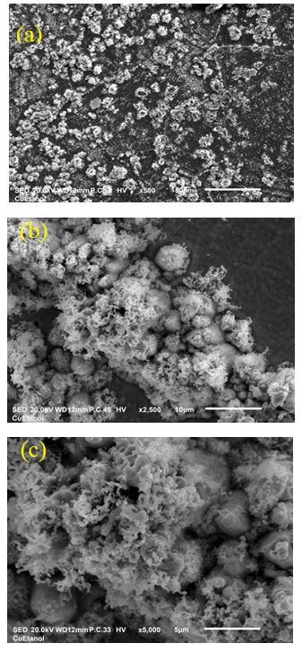 Figure 3. SEM micrographs of thin CNx deposited by pulsed discharge at a pressure of 1 Torr, taken at (a) 10X, (b) 50X, and (c) 1000X magnification..
3.3. AFM analysis
Figure 4 shows the three-dimensional (3D) AFM images of the deposited thin-film using a current of 300 mA. Figures 4(a), 4(b), and 4(c) show results obtained by AFM at different scales in contact mode that is, at swept lines of 50, 25, and 10 mm, respectively. The morphology that occurs in the deposited films is determined by the non-uniformity in the surface morphology, which can be explained by the presence of large graphitic domains and a polymer component of CN.
Higher polymer components lead to a smoother film, whereas higher graphite-cluster contents and larger cluster sizes lead to more agglomerations [23]. A large polymeric component results in low roughness, whereas a greater number of graphitic clusters induce the formation of more or larger agglomerations. Although no defined grains were observed on the surfaces of the films, we have established that the CNx films had linear and graphite-like polymer components, which could lead to the surface non-uniformity. These results agree with those presented by A. Stanishevsky [25] regarding the morphology of CNx films.
The microstructure, in addition to the morphology formed during thin-film formation, are important issues in determining the mechanical (hardness and elastic recovery) and tribological properties (friction coefficient and wear rate) of CNx films [26]. Therefore, such thin films could be important materials for application in many tribological uses, because of their mechanical properties, and in solar cells, due to their optical and electrical properties [27]. Another interesting application of the present work is that the observed morphology determined the non-uniformity in the surface that effect could be reproduce using phase-field model for planer film surface [28], by the corresponding different nanoscale effects [29], or by thin planar interfacial models [30, 31].
3.4. Plasma analysis
Figure 5 display the OES spectrum for CH3CH2-N2 in the spectral range of 200–900 nm. In the mixture, decomposition of CH3CH2OH takes place by breaking the C-H chemical bonds in the discharge, producing atomic and molecular impacts and excitation reactions between radicals and N atoms. The species observed are as follows: Swan bands (d3Pg – a3Pu), which are characteristic of the C2 molecule at 473.71 nm (Dn = +1), 516.52 nm (Dn = 0), and 563.55 nm (Dn = −1) [16], and CN violet bands (B2S+ – X2S+), for which the band heads appear at 359.04 nm (Dn = +1), 388.34 nm ( ), and 421.60 nm (Dn = −1). Here Dn = n′ − n″ is the difference in vibrational quantum numbers between the upper (n′) and lower (n″) transition states. Also seen are CH (B2S-X2P) at 390 nm and CH (A2D-X2P) at 426.76 nm.
Figure 6 shows CN, N2, and Hb emissions observed in the plasma discharge. The N2 (B3Pg–C3Pu) band, which corresponds to the second positive system (SPS, 337.1 nm), may be mainly due to the presence of two consecutive reactions: (1) the electron impact excitation of the N2 molecular energy ground state and (2) radiative decay to a lower level with the emission of a characteristic photon. These reactions are respectively expressed as
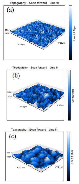 Figure 4. AFM images of thin CNx deposited by pulsed discharge at a pressure of 1 Torr, taken at different scales. (a) 50 mm; (b) 25 mm; (c) 10 mm
N2( 1 +g) N2( 3 u) + e (1)
and
N2( 3 u) N2( 3 g) + hv (337.1 nm) (2)
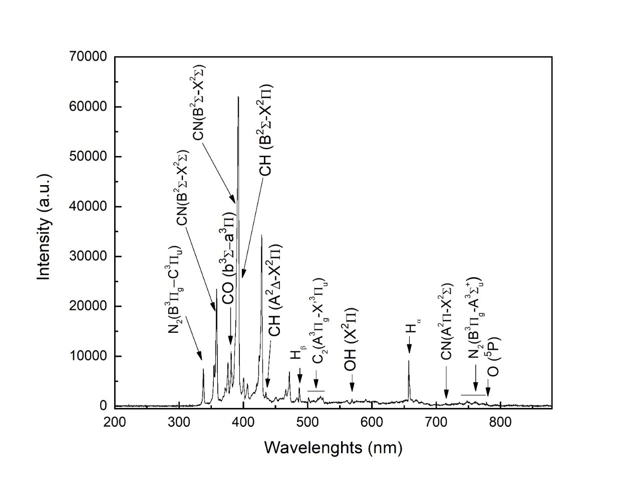 Figure 5. OES CH3CH2OH/N2 plasma.
The interactions of N2 species with C2H5OH lead to the formation of CN species [32]. The violet and red spectral systems of CN are shown in Figure 6.
The violet spectral system of CN may be produced by the following reaction:
![]()
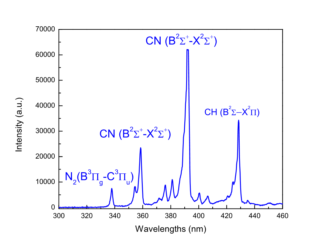 Figure 6. OES spectrum CN, N2 and CH species.
which corresponds to Dn = 0 and a radiative lifetime t = 60 ns. The resulting vibrational distribution of CN (X2S+) can be modified by relaxation processes that include vibrational collision relaxation within each electronic state, inter-electronic transfer by collision between vibrational levels of the states X2S+ and A2P, and the radiative deexcitation of the vibrational levels of A2P toward vibrational levels lower than the X2S+ state. The latter of these relaxation processes result in the appearance of the red spectral system, as shown in Figure 7, and is expressed as
![]() with Dn = 3 and a radiative lifetime t = 6000 ns.
with Dn = 3 and a radiative lifetime t = 6000 ns.
Conversely, from Figure 5 it can be seen that the CN species at 388.3 nm and the N2+ species at 390 nm overlap, implying that the production of CN radicals in that interval is mainly linked to the excited state of N2 (C3Pu). This phenomenon has two causes: (i) resonant excitation in collisions between highly excited neutral N2 molecules (3.26 eV) and CN radicals (3.19 eV) or (ii) the high energy of the excited N2 (11.1 eV) favoring the generation of atomic N, which in turn favors CN formation. The reaction of N atoms with C or C-containing species is exothermal, which facilitates these reactions [33–35]. N atoms within the discharge could not be detected because their lifetimes are shortened by bonding with N atoms and C-containing species.
Its peaks are also covered up by CN compounds with higher intensities. The presence of CN radicals within the discharge is mainly related to the excited state of N2 [32]. C2 Swan band emissions arise from transitions between electronic states (d3Pg–a3 Pu) as a probable result of the dissociation of CH3CH2OH in the following way:
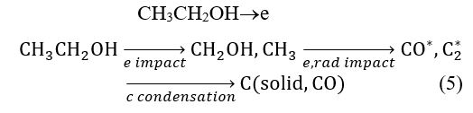
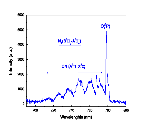 Figure 7. OES spectrum CN (red spectral system), N2 and O atom species.
As can be seen in (5), atomic hydrogen is removed from CH3CH2OH [32, 36] and the C-C bond finally dissociates by direct electron impact, which leads to the formation of solid carbon. The presence of C2 can be taken as an indication of solid carbon formation, as it is known that the C2 species initially nucleates in solid carbon clusters [37]. This would result in the presence of C2 Swan bands in the range of 480–530 nm.
Swan band heads correspond to (0,0), (1,1), (2,2), (3,3), and (4,4) with a Dn = 0. Carbon molecules react with N atoms in the following way:
N + C2 CN + C (6)
We assume that generation of C2 molecules was caused by collisions in the plasma, which promote recombination of the dissociated C of the CH5 species. The C2 species and the CN radicals generated within the mixture contribute to the growth of the CN thin films. The availability of C2 species provides a considerable fraction of sp2 hybridization, as opposed to sp3 hybridization, which is an important factor in the formation of graphite-like or fullerene-like structures with sp2 hybridization in deposited CN films.
The emission of CH (B2S+–X2P) at 388.9 nm becomes embedded in the CN signal, as seen in Figure 5. The presence of CH in the CH3CH2OH discharge can be considered an indication of solid carbon and higher order hydrocarbon formation. This is because CH species are typically found as intermediate radicals in the formation of these products [36]. CH species react with nitrogen atoms in the following process:
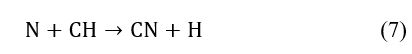 However, CH radicals can arise as intermediate reaction products to generate CH4, C2H2, C2H4, C2H6, or C3H8 [38, 39] when hydrogen atoms (Ha and Hb) react with solid carbon fragments [40–42]. The presence of Ha and Hb in the discharge is a result of (7), which forms the hydrogen species. In Figure 5, these species are seen as the most intense lines of the Balmer series.
The presence of Ha and Hb is related to dissociation of the CH and OH within the discharge, as seen in (7) and (8), which could also be a new source for hydrogen generation.
4. Conclusions
CNx thin films were deposited on Cu substrates using a pulsed discharge method with CH3CH2OH as the source of carbon and N2 as the sputtering ion and nitrogen source.
Through Raman analysis, it was demonstrated that the structure of the deposited films was amorphous. The characteristic Raman D and G peaks for carbon were identified. The position of the G peak is related to the vibrational energy of the present bonds; therefore, there is a shift toward higher frequencies due to the decrease of sp3 bonds and hence the increase in sp2 bonds. This indicates that a conversion of sp3 bonds to sp2 bonds occurred in the CNx films owing to the increase in temperature. Such a conversion process could form large graphite domains with large size and/or an increased number of sp2 clusters, eventually leading to graphitization. The observed high-frequency D peak shift, on the other hand, suggested densification of ringed sp2 in the atomic network, also increasing the sp2-bond content. In addition, the Raman analysis showed an additional band centered at approximately at 2250 cm−1, which appears because of the stretching vibration of a triple bond C-N. This suggests that the C and N atoms are chemically bonded in the film. An ID/IG value of 1.32 suggested that C sp2 is more likely to have formed in the film, considering that C=C and/or C=N bonds can be formed in rings and there are fewer opportunities to form C=C and/or C=N links in chains. In addition, this ID/IG value indicated the growth of the graphitic domains or the increase of their number, i.e., graphitization by heating with an increase in disorder of the angles of the bonds of the C and N atoms sp2 in the films.
Through SEM analysis, we were able to observe the thin-film morphology, wherein carbon clusters deposited on the surface of the Cu were observed. The lack of uniformity of the non-homogeneous surface can be attributed to the distance between the electrodes during the deposition process. Since the deposition rate is considered proportional to the distance, these observed agglomerations cause the formation of large islands with small grains, in turn generating an irregular surface. These results were later corroborated with AFM results, from which we determined the morphology of the CNx film. The surface was found to lack uniformity, which can be explained by the presence of large graphite domains and a polymeric component of CN. This reveals that the greater the content of graphite groups or the larger their size, the greater the number of agglomerations. Finally, we conclude that the films grow via island growth, very similar to the results presented by A. Stanishevsky [25].
OES measurements confirmed the decomposition of the CH3CH2OH molecule as a result of electron impact dissociation in the plasma discharge. Products obtained from the dissociation collide with the N species to generate CN radicals and form violet
and red emission spectra characteristic of CN. CN radicals are important because of their variety of industrial applications, mainly in materials science. In addition, the C2 Swan band, a species that also plays an important role in the appearance of CN radicals, was identified. The presence of CH indicated the formation of solid carbon. Hydrogen species were also detected in the CH3CH2OH-N2 plasma mixture. Therefore, the mixture plasma is not only useful for producing CN but also for generating hydrogen.
Conflict of Interest
The authors declare no conflict of interest.
Acknowledgment
We are grateful to the Advanced Physics Laboratory (FC/UAEM), Spectroscopy laboratory (ICF/UNAM) and TESJo for their infrastructure provided to carry out the research. This research was supported by CONACyT scholarship for doctoral study, DGAPA[IN102222], CONACyT [225991 and 268644] and UAEM [4307/2017/CI].
- M. Uz A. Y. Liu, M. L. Cohen, (1992), Theorical study of a hypothetical metallic phase of carbon, Phys. Rev. B, 45, 4579-4581. https://doi.org/10.1103/PhysRevB.45.
- Y. Bu, Z. Chen, J. Yu & W. Li, (2013), A novel application of g-C3N4 thin film in photo-electrochemical anticorrosion, Electrochim. Acta., 88, 294-300. https://doi.org/10.1016/j.electacta.2012.10.049
- Yan, S. C., Li, Z. S. & Zou, Z. G., (2009), Photo-degradation Performance of g-C3N4 Fabricated by Directly Heating Melamine, Langmuir, 25, 10397-10401. https://doi.org/10.1021/la900923z
- F. K. Kessler; Y. Zheng; D. Schwarz; C. Merschjann; W. Schnick; X. Wang; M. J. Bojdys, (2017), Functional carbon nitride materials- design strategies for electrochemical devices, Nature Reviews Materials, 17030. https://doi.org/10.1038/natrevmats.2017.30
- K. Schwinghammer, M. B. Mesch, V. Duppel, C. Ziegler, J. Senker and B. V. Lotsch, (2014), Crystalline Carbon Nitride Nanosheets for Improved Visible-Light Hydrogen Evolution, J. Am.Chem.Soc.,136, 5, 1730-1733. https://doi.org/10.1021/ja411321s
- J. Xu, M. Antonietti, and M. Shalom, (2016), Moving Graphitic Carbon Nitride from Electro-catalysis and Photo-catalysis to a Potential Electrode Material for Photoelectric Devices, Chem. Asian J., 11, 2499-2512. https://doi.org/10.1002/asia.201600857
- Ravinder Kour, Sandeep Arya, Sheng-Joue Young, Vinay Gupta, Pankaj Bandhoria, and Ajit Khosla, (2020), Review-Recent Advances in Carbon Nanomaterials as Electrochemical Biosensors, Journal of The Electrochemical Society, 167 037555. https://doi.orfg/10.1149/1945-7111/ab6bc4
- H. Yu, P. Li, J. Robertson, (2011), Fabrication and bio-functionalization of tetrahedral amorphous carbon thin films for bio sensor applications, Diamond & Related Materials, 20, 1020-1025. https://dx.doi.org/10.1016/j.diamond.2011.06.005
- Z. A. Umar, R. S. Rawat, R. Ahmad, Z. Chen, Z. Zhang, J. Siddiqui, A. Hussnain, T. Hussainc and M. A. Baiga, (2017), Structural, compositional and hardness properties of hydrogenated amorphous carbon nitride thin films synthesized by dense plasma focus device, Surface and Interface Analysis, 49, 548-553. https://doi.org/10.1002/sia.6192
- P. Wang, T. Takeno, K. Adachi, H. Miki & T. Takagi, (2012), Preparation and tribological characterization of amorphous carbon nitride coatings in a RF PECCVD-DC PVD hybrid coating process, Applied Surface Science, 258, 6576-6582. https://doi.org/10.1016/j.apsusc.2012.03.082
- Nicolas D. Boscher, Florian Hilt, David Duday, Gilles Frache, Thierry Fouquet, Patrick Choquet, (2015), Atmospheric Pressure Plasma Initiated Chemical Vapor Deposition Using Ultra-Short Square Pulse Dielectric Barrier Discharge, Plasma Process. Polym., 12, 66-74. https://doi.org/10.1002/ppap.201400094
- N. Nedfors, Oleksiy Vozniy, and Johanna Rosen, (2018), Effect of synchronized bias in the deposition of TiB2 thin films using high power impulse magnetron sputtering, J. Vac. Sci. Technol. A, 36, 3. https://doi.org/10.116/1.5003194
- Asim Aijaz Kostas Sarakinos, Mohsin Raza, Jens Jensen and Ulf Helmersson, (2014), Principles for designing sputtering-based strategies for high-rate synthesis of dense and hard hydrogenated amorphous carbon thin films, Diamond and Related Materials. Vac., 44, 117-122. https://doi.org/10.1016/j.diamond.2014.02.014
- Yuyang Kang, Yongqiang Yang, Li-Chang Yin, Xiangdong Kang, Gang Liu, and Hui-Ming Cheng, (2015), An Amorphous Carbon Nitride Photo-catalyst with Greatly Extended Visible-Light-Responsive Range for Photo-catalytic Hydrogen Generation, Adv. Mater., 27, 4572-4577. https://doi.org/10.1002/adma.201501939
- R O Dillon, J Woollam, V Katkanant, (1984), Use of Raman scattering to investigate disorder and crystallite formation in as-deposited and annealed carbon films, Phys. Rev. B, 29, 3482. https://doi.org/10.1103/PhysRevB.29.3482
- Y Taki, T Kitagawa, O Takai, (1997), Shielded arc ion plating and structural characterization of amorphous carbon nitride thin films, Thin Solid Films, 304, 183-190. https://doi.org/10.1016/S0040-6090(97)00193-4
- A C Ferrari, S E Rodil, J Robertson, (2003), Interpretation of infrared and Raman spectra of amorphous carbon nitride, Phys. Rev. B, 67, 155306, 155. https://doi.org/10.1103/PhysRevB.67.155306
- H Jung, H Ho Park, (2000), Studies on the structure and bonding state of nitric amorphous carbon (a-CNx) films by reactive rf magnetron sputtering, Thin Solid Films, 377-378, 320-325. https://doi.org/10.1016/S0040-6090(00)01363-8
- J. Wang, N. Huang, C. J. Pan, S.C.H. Kwok, P. Yang, Y.X. Leng, J. Y. Chen, H. Sun, G. J. Wan, Z. Y. Liu and P. K. Chu, (2004), Bacterial repellence from polyethylene terephthalate surface modified by acetylene plasma immersion ion implantation-deposition, Surface and Coatings Technology, 186 (1-2), 299-304. https://doi.org/10.1016/j.surfcoat.2004.02.046
- E. Cappelli, C. Scilletta, S. Orlando, V. Valentini and M. Servidori., (2009), Laser annealing of amorphous carbon films, Applied Surface Science, 255, 5620-5625. https://doi.org/10.1016/j.apsusc.2008.10.062
- L. Marcinauskas, A. Grigonis, P. Valatkevicius and A. Medvid, (2012), Irradiation of the graphite-like carbon films by ns-laser pulse, Applied Surface Science, 261, 488-492. https://doi.org/10.1016/j.apsusc.2012.08.042
- X. Wang, Z. Li, P. Wu, E. Jiang and H. Bai, (2006), Annealing effects on the microstructure of amorphous carbon nitride films, Applied Surface Science, 253 (4), 2087-2092. https://doi.org/10.1016/j.apsusc.2006.04.003
- R. Maeda & K. Kikuch, (1997), Deposition of thin films by uv light laser ablation, Surf. Eng., 13,71-74. https://doi.org/10.1179/sur.1997.13.1.71
- Ming Gao, Danni Liu, Huanhuan Yang, Hao Huang, Qian Luo, Yifan Huang, Xue-Feng Yu and Paul K.Chu, (2019), Modification of Layered Graphitic Carbon Nitride by Nitrogen Plasma for Improved Electrocatalytic Hydrogen Evolution, Nanomaterials, 9, 568. https://doi.org/10.3390/nano9040568
- A. Stanishevsky, (1998), On the surface morphology of C: N films deposited by pulsed cahodic arc discharge method, Mater. Lett., 37, 162-167. https://doi.org/10.1016/S0167-577X(98)00085-8
- E. Broitman et al., Mechanical and tribological properties of CNx films deposited by reactive magnetron sputtering, Wear, 248, 55-64. https://doi.org/10.1016/S00431648(00)00519-6
- Z. B. Zhoua, R. Q. Cui, Q. J. Pang, G. M. Hadi, Z. M. Ding, W. Y. Li, (2002), Schottky solar cell with amorphous carbon nitride thin films prepared by ion sputtering technique, Solar Energy Materials & Solar Cell, 70, 487-493. https://doi.org/10.1016/S0927-0248(01)00086-1
- A. M. Roy, (2021), Barrierless melt nucleation at solid-solid interface in energetic nitramine octahydro-1, 3, 5, 7-tetrazocine, Materialia, 15, 101000. https://doi.org/10.1016/j.mtla.2021.101000
- A. M. Roy, (2021), Influence of Nanoscale Parameters on Solid-Solid Phase Transformation in Octagen Crystal: Multiple Solution and Temperature Effects, JETP Letters, 113 (4), 265-272. doi.org/10.1134/S0021364021040032
- A. M. Roy, (2021), Formation and stability of nanosized, undercooled propagating intermediate melt during phase transformation in HMX nanocrystal, Europhysics Letters, 133, 56001. doi: 10.1209/0295-5075/133/56001
- A. M. Roy, (2021), Energetics and kinematics of undercooled nonequilibrium interfacial molten layer in cyclotetramethylene-tetranitramine crystal, Physica B: Condensed Matter, 615, 412986. https://doi.org/10.1016/j.physb.2021.412986
- E. Tatarova, N. Bundaleska, F. M Dias, D. Tsyganov, R. Saavedra and C. M. Ferreira, (2013), Hydrogen production from alcohol reforming in a microwave ‘tornado’-type plasma, Plasma Sources Sci. Technol., 22. 065001. https://doi.org/10.1088/0963-0252/22/6/065001
- K. J. Clay, S. P. Speakman, G. A. J. Amaratunga, and S. R. P. Silva, (1996), Characterization of a-C:H:N deposition from CH4/N2 rf plasmas using optical emission spectroscopy, J. Appl. Phys., 79 (9),7227-7233. https://doi.org/10.1063/1.361439
- S. Veprek, J. Weidmann and F. Glatz, (1995), Plasma chemical vapor deposition and properties of hard C3N4 thin films, J. Vac. Sci. Thechnol., 13, 2914. https://doi.org/10.1116/1.579613
- Wei Hu, Jun-Yi Tang, Jia-da Wu, Jian Sun, Yi-qun Shen, Xiao-feng Xu, and Ning Xu, (2008), Characterization of carbon nitride deposition from CH4/N2 glow discharge plasma beams using optical emission spectroscopy, Physics of plasma, 15, 073502. https://doi.org/10.1063/1.2953521
- A. Yanguas-Gil, J. L. Hueso, J. Cotrino, A. Caballero, and A. R. González-Elipe, (2004), Reforming of ethanol in a microwave surface-wave plasma discharge, Appl. Phys. Lett., 85,4004-4006. https://doi.org/10.1063/1.1808875
- A. Kumar, P. A., A. Xue, B. Hao , Y. K. Yap and R. M. Sankaran, (2013), Formation of nanodiamonds at near-ambient conditions via micro-plasma dissociation of ethanol vapour, Nature Communication, 4, 2618. https://doi.org/10.1038/ncomms3618
- J. Serrano, J. Moros and J. J. Laserna, (2015), Exploring the formation routes of diatomic hydrogenated radicals using femtosecond laser-induced breakdown spectroscopy of deuterated molecular solids, J. Anal. At. Spectrom., 30, 2343-2352. https://doi.org/10.1039/C5JA00192G
- G. M. Harris and A. W. Tickner, (1947), Reaction of Hydrogen Atoms with Solid Carbon, Nature, 160 ,871. https://doi.org/10.1038/160871a0
- A. Okita, Y. Suda, A. Ozeki, H. Sugawara, Y. Sakai, A. Oda, and J. Nakamura, (2006), Predicting the amount of carbon in carbon nanotubes grown by CH4 RF plasmas, J. Appl. Phys., 99, 014302. https://doi.org/10.1063/1.2150599
- A. Okita, Y. Suda, A. Oda, J. Nakamura, A. Ozeki, K. Bhattacharyya, H. Sugawara, and Y. Sakai, (2007), Effects of hydrogen on carbon nanotube formation in CH4/H2 plasma, Carbon, 45, 7, 1518-1526. https://doi.org/10.1016/j.carbon.2007.03.022
- A. Oda, Y. Suda, and A. Okita, , Numerical analysis of pressure dependence of carbon nanotube growth in CH4/H2, Thin Solid Films, 516,19, 6570-6574. https://doi.org/10.1016/j.tsf.2007.11.088
Citations by Dimensions
Citations by PlumX
Google Scholar
Crossref Citations
No. of Downloads Per Month
No. of Downloads Per Country