Light Modulation Enhancement by using an Impedance Matching Scheme for a Subcarrier Multiplexed Light Transmitter

Adv. Sci. Technol. Eng. Syst. J. 6(6), 07–11 (2021);
 DOI: 10.25046/aj060602
We propose and analyze new impedance matching schemes to enhance applied voltage to an optical modulator and light modulation for a subcarrier multiplexed light transmitter or a radio-on-fiber transmitter that carries radio-frequency signal through an optical fiber. Our proposal includes two methods using a quarter-wavelength impedance transformer and a tapered microstrip line for impedance matching between a driver circuit and an electro-absorption modulator. Simulation results for both two schemes show that large enhancement is observed for 20 GHz and lower frequency and that some resonant boosts are observed for higher frequency as well. Discussions are described to design a circuit with improved performances. It is shown that our schemes can drive the electro-absorption modulator at a voltage higher than 1 V that is sufficient to drive the modulator.
1. Introduction
The use of optical fiber network has become more popular to send both broadband digital data [1] and modulated radio frequency (RF) signal [2]. The latter is referred to as radio-on-fiber (RoF) technology, where the signal is transmitted as subcarrier-multiplexed (SCM) laser light. The digital network requires optical devices such as a laser diode (LD), a light modulator, and a photodiode to have broadband response. In contrast, the RoF network does not require such broadband response but requires only a few spot-frequency or segmented-frequency responses. Such RoF systems are employed in a network between a data center and an access point for cellular services, where radio carrier frequency becomes higher, especially at the fifth generation cellular services using a Ka-band [3]. In addition to these services, some satellites employ a Ku-band so that the use of optical fiber link is practical between an antenna and a control site in an earth station. For example, some small cube satellites, developed by universities and consortiums, sent the Ku-band signals to earth stations in its downlink system [4]. A RoF link was employed in the earth station to reduce RF signal loss in conventional coaxial cables [5-7]. In addition to the low link loss, the optical fiber will benefit us in many aspects such as weight and cost.
To achieve a higher frequency operation and to avoid chromatic dispersion in an optical fiber, an electro-absorption modulator integrated laser diode or an externally modulated laser (EML) would be one of the strong candidates to develop a SCM transmitter. The EML is monolithic integration of an electro-absorption modulator (EAM) and a distributed feedback laser diode (DFB-LD), as shown in Figure 1. A current source is connected to the DFB-LD to obtain continuous laser light and a digital or a RF source to the EAM to obtain modulated light. The EML emits SCM light when the RF signal is applied to the EAM. Both the optical devices can concentrate on either high-speed modulation or single-mode emission of laser light [8, 9]. Most EMLs are designed for 1.5-mm wavelength networks and are widely used in commercial optical networks due to their performances, compactness, and reliability. In addition to the commercial optical networks, they are applied to the shorter-length, high-throughput Ethernet services [10-12], which makes an optical transmitter smaller in size and compatible with optical transmitter standards. Challenges have been done to develop a 1.3-mm wavelength device [11].
A link length limit due to chromatic dispersion has been analyzed for the RoF link in the satellite earth station that employs the EML [13], which is different from the digital network systems. Effort has been made to achieve a more-functional device such as radio frequency conversion in the SCM light [14].
One of the interesting approaches to enhance the response of EMLs is the use of via connection in three-dimensional substrate to mount the EML [12]; however, this technique needs the state-of-the-art manufacturing process. On the other hand, this paper focuses on a passive transmission line between a RF source and the EAM, as shown in Figure 2. The EAM is a reversely biased diode with an external resistive load of 50 W in general. The conventional 50-W matching may be a bottle neck for driving the device. Our idea to overcome this issue is a simple matching scheme such as a quarter-wavelength impedance transformer (QIT) and a tapered microstrip line (TML) that can match the driver and the modulator with different impedance [15-17]. Hence, we can increase the external load resistance to increase the applied voltage to the modulator and its modulation index.
Our proposed scheme is described in Section 2 and some results in Section 3. We discuss characteristics and features of the QIT and TML in Section 4. We will conclude this paper in Section 5.
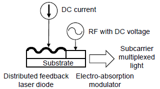 Figure 1: Cross Section of an Electro-Absorption Modulator Integrated Laser Diode (EML) and Power Sources
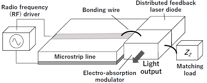 Figure 2: Schematic Model Including a RF Source, a Transmission Line, and an EML
1. Proposed Structure and Circuit Model
A circuit around the EML is shown in Figure 2. A RF signal is transferred from a RF driver to the EAM in the EML through a microstrip line. Impedance of the driver, the EML, and the microstrip line is 50 W in general. We should notice the reversely biased EML has very high impedance but it can be impedance-matched by using an external parallel resistance of approximately 50 W. We could choose favorite impedance if the entire circuit can be matched by other methods. We propose the use of QIT and TML that are shown in Figure 3 (a) and (b), respectively. The QIT must follow equation below
Z02 = Z1 Z2 (1)
where Z0 is microstrip line impedance, and Z1 and Z2 impedance of the RF driver and the parallel load to the EAM, respectively, and the microstrip line length must be a quarter of a wavelength (l/4) or multiplied length by odd numbers (3l/4, 5l/4…). If the TML is long enough and if the impedance at the both end matches with adjacent circuits, no electric reflection occurs at the boundaries.
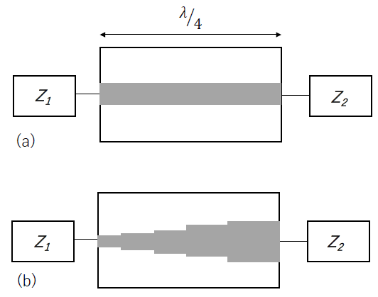 Figure 3: Structure of the Transmitter with (a) a Quarter-Wavelength Impedance Transformer (QIT) and (b) a Tapered Microstrip Line (TML).
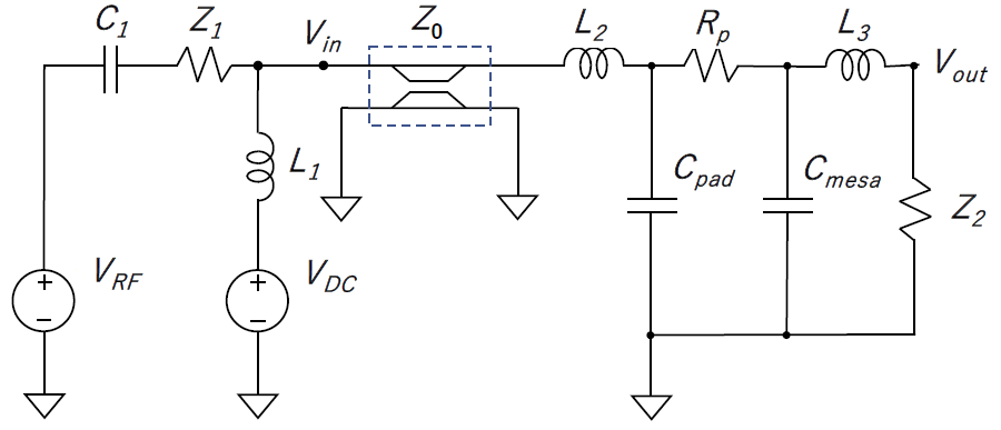 Figure 4: Equivalent Circuit Consisting of a RF Source, a Transmission Line, and an EAM.
Figure 4 shows the entire equivalent circuit of the driver, the RF transmission line and, the EAM. A symbol, VRF, on the left hand with its load impedance Z1 is the RF driver and the next the reverse voltage source, where the both sources are connected to a RF line Z0 through a bias-tee of C1 and L1. The RF line Z0 is placed on the center to connect the RF source and the EAM. All the electric signals, dc and ac, pass through Z0 to the EAM section consisting of two inductors, one resistor, and two capacitors; L2 and L3: inductances of bonding wires to the microstrip and to the external load, respectively, Rp: a resistance of electrode, Cmesa: a capacitance of the modulator diode, and Cpad: a capacitance of an electrode pad. An external matching resistive load Z2 is connected to the EAM in parallel. In our simulation, we used the values as follows: VRF=1 V, Rp =5 W, L1=79.4 mH, L2=0.11 nH, L3=0.04 nH, C1=51 nF, Cpad=0.029 pF, Cmesa=0.45 pF. These values have been obtained from measurements or theoretical calculations. Other parameters will be described when they are needed. We assumed the central operation frequency to be 28 GHz, one of the fifth generation cellular service bands. We analyzed the proposed circuits by using a circuit simulator LTspice. A tapered microstrip line circuit model was not available so that cascaded, stepped microstrip line (Tline) models, shown, in Figure 3(b), were employed instead. The number of steps was five. As a result, we were able to use the LTspice circuit models including Tline for all the components. Any commercially available substates were not assumed except for MEGTRON7 to have general discussions in this paper.
If we assume that the DFB-LD in the EML is operated with an automatic-power-control current supply, the DFB-LD emits continuous single-mode laser beam. The EAM modulates the laser beam into SCM laser light that carries information of RF signal.
2. Simulation Results
2.1. Results for Quarter-wavelength Impedance Transformer
Assuming a dielectric constant of the substrate as 3.4 and the output impedance of EML, Z2, as 50 (gray), 70 (blue), or 100 W (orange), we calculated terminal voltage spectra for circuits with QIT, as shown in Figure 5. Here, the impedance of the RF driver, Z1, can be calculated as 50, 35.7, or 25 W by using Eq. (1). The terminal voltage is defined by the voltage across the EAM. The voltage at the lower frequency or at the left edge in Figure 5 is higher for the higher impedance and the enhancement ratio is nearly proportional to Z2. This tendency can be found at most of the frequency ranges between 1 and 20 GHz. The enhancement is obtained simply due to higher voltage division in Z2. The voltage curves decrease as the frequency becomes higher in a case, Z2 = 50 W, which is the same with the conventional structure, while some peaks are found for Z2 of 70 and 100 W. The peaks are obtained at 6.1, 30, 60, and 92 GHz for Z2 of 100 W. In addition to the simple boost of the voltage in the lower frequency range, we obtained response peaking in the higher frequency range, which is due to resonance by some inductive and capacitive elements.
We obtained powerful voltage boost by using the QIT microstrip line between the driver and the EML with the load impedance higher than 50 W, as expected. The resonant peaks enable the applied voltage boost at three or four frequencies.
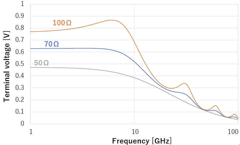 Figure 5: Spectra of the Terminal Voltage across the EAM when the QIT is Employed.
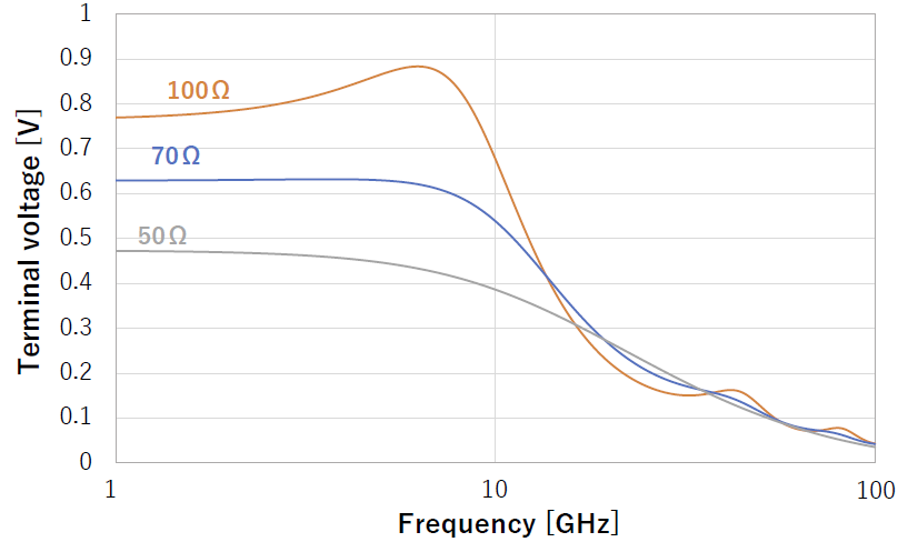 Figure 6: Spectra of the Terminal Voltage across the EAM when the TML is Employed.
2.2. Results for Tapered Microstrip Line
Figure 6 shows the calculated terminal voltage spectra for the circuit including the TML. The results are the same with the results of QIT circuit qualitatively. In the lower frequency range, the terminal voltage is amplified with magnification of Z2/Z1 approximately, which means that we can obtain higher voltage from the higher impedance of Z2. In the higher frequency range, fewer number of resonant peaks are found and their amplitudes are smaller even if they exist. The peak at 6.4 GHz is observed as very similar to the results of QIT while two lower peaks are observed at 41.7 and 79.8 GHz for Z2 of 100 W.
When we have to determine which circuit we should adopt, we have to note that both will function at the same performance for frequencies lower than 20 GHz but that the details differ between the QIT and the TML. The QIT exhibits a higher voltage or a high light modulation index when we manufacture all the devices and a circuit, as specified and as designed. If we are not able to manufacture the devices as specified nor as designed, the TML would be a good choice since it allows some margin in the resonant frequencies to provide lower and broader peaks.
For clearer comparison, we show terminal voltage dependence on the load impedance Z2 for a frequency at 1 GHz (blue), the first resonant frequency near 6 GHz (orange), and the second resonant frequency near 30 GHz (gray) in Figure 7. The plots and lines are overlapped for the two models of QIT and TML at 1 GHz and the first resonant frequency while they differ at the second resonant frequency.
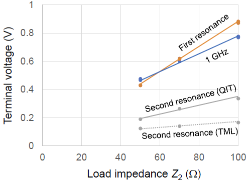 Figure 7: Terminal Voltage Dependence on the load impedance Z2.
The terminal voltages always increase as the load impedance becomes higher. All the lines are linear in a Z2 range between 50 and 100 W; however, the number of calculated points of the load impedance is limited to only three. Thus, we can double the voltage at 1GHz and the first resonant frequency when we employ a load impedance of 100 W other than the original 50 W. When we pay our attention to the second resonance, we should choose the QIT model (solid line) since it provides much higher voltages than the TML model (broken line). In both cases, the terminal voltages are even higher with the 100-W load than the voltages with the original 50-W load. Our ideas are worth applying to the optical transmitter especially when we consider that the second resonant frequency, 30 GHz, is within the fifth-generation cellular service band.
3. Discussion
Difference of the improvement between the two proposed structures, QIT and TML, is small at a 20-GHz frequency and lower. However, we should analyze the results in the previous section for better performance at higher frequencies. Resonant frequency dependences on the order of the resonance are shown in Figures 8 and 9 for the QIT and TML, respectively. We plotted these figures, assuming dielectric constants to be 3.4, 10, and 15, where some parameters of MEGTRON7 were adopted for the constant of 3.4. We took account of dielectric losses due to the substrates. The load impedance to the EML, Z2, was assumed to be 100 W. The number of the orders is larger within the plotted frequency range as the dielectric constant becomes larger. The number of plotted points are three, four, and, five for dielectric constants of 3.4, 10, and, 15, respectively, as shown in Figure 8. The relationship between the resonant frequency and the order is close to a linear function. The number of the points for the QIT is larger than that for the TML. We obtained the dependency on the dielectric constant, the order of resonant peak, and the type of the matching structure, which provides us more flexibility in designing and manufacturing the matching circuits.
The results described above focus only on the resonant frequency; however, the terminal voltage at a resonant frequency is of importance as well. Figures 10 and 11 show a voltage across the EAM versus a resonant frequency for the QIT and TML, respectively. The employed parameters are the same with those for Figures 8 and 9. The figures include results for the conventional 50-W-matching circuit. The curves are overlapped for all the three dielectric constants and the voltages are inversely proportional to the logarithmic plot of the frequencies, as shown in Figure 10. At a 30-GHz frequency near the fifth generation cellular band, the terminal voltage of 0.34 V is achieved for all the dielectric constants. We obtained only 0.2 V from the conventional structure in contrast. Similar results are obtained for the TML, as shown in Figure 11. Here, we have to note the terminal voltages are dependent on a dielectric constant at the TML model. The lower dielectric constant substrate provides us higher voltage.
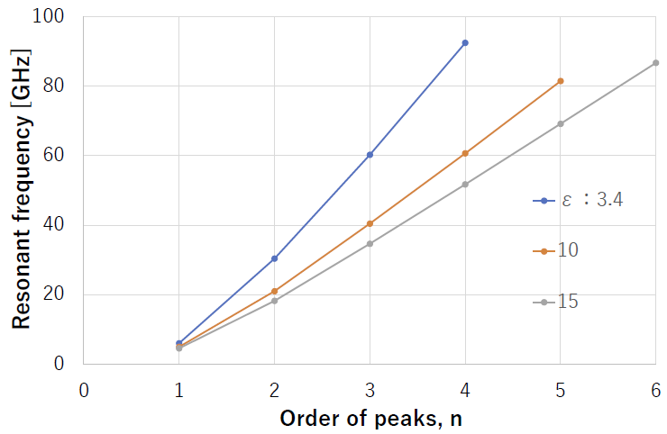 Figure 8: Resonant Frequency Dependence on the Order of Peak for the QIT Model.
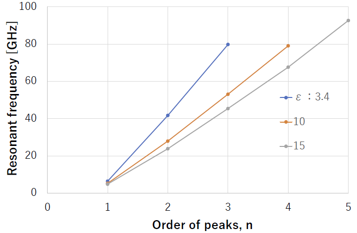 Figure 9: Resonant Frequency Dependence on the Order of Peak for the TML Model.
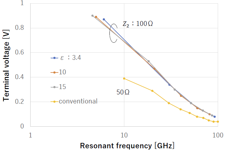 Figure 10: Terminal Voltage across the EAM versus Resonant Frequency for the QIT Model.
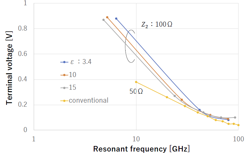 Figure 11: Terminal Voltage across the EAM versus Resonant Frequency for the TML Model.
Numeric analysis has been successfully done for the proposed structure that employs a higher impedance load in parallel to the EAM. In addition, we analyzed the behavior at higher impedance, Z2, for the QIT. Figure 12 shows a terminal voltage dependence on a resonant frequency for the QIT circuit with the impedance Z2 of 500 W. The tendency is similar qualitatively with the previous results. It should be noted that the terminal voltage becomes approximately 5.5 times those obtained from the conventional circuit. The voltages at resonant frequencies 30 and 60 GHz are 1.05 and 0.52 V, respectively, which are sufficient to drive the EML and to transmit the SCM laser light. This trial may not be applied to the TML model unfortunately since such a high-impedance microstrip line cannot be fabricated on a typical substrate.
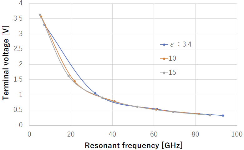 Figure 12: Terminal Voltage across the EAM versus Resonant Frequency for the QIT Model, Assuming the Load Impedance, Z2, is 500 W.
4. Conclusions
We have proposed new structures to boost applied voltage to the EAM and its modulation index in a SCM or RoF transmitter that carries radio-frequency signal through an optical fiber. The two proposed models employ a QIT and a TML, both are capable of impedance matching for two adjacent devices with different impedance. Our analysis has been done numerically by using an electronic circuit simulator. Comparing with the conventional circuit, the voltage applied to the modulator increases approximately at the ratio of the load impedance to the transmission line impedance at 20 GHz and lower frequency in both the structures. Due to the capacitive and inductive elements in a circuit, some resonant peaks were found at higher frequency in both the models. The applied voltage to the EAM is enhanced at the resonant frequencies.
To further improve performances, we have analyzed characteristics of our models with parameters of dielectric constant of substrates and load impedance. The results are similar between the two models. The impedance of the QIT microstrip line is constant and a standard one of 50 W. On the other hand, the impedance must be varied in a wide range from Z1 to Z2 on a TML substrate, which might be difficult to fabricate in some cases. We should note the matter described above in designing a circuit.
It is finally concluded our proposal does not require any active device but that it can enhance the voltage across the EAM and modulation index of the SCM light. This technique would be easily applied to most of the light transmitters such as a direct modulation laser and a Mach-Zender light modulator. In addition, this kind of RoF link would be applied to higher-frequency applications [18].
Conflict of Interest
The authors declare no conflict of interest.
Acknowledgment
This work was supported by JSPS KAKENHI Grant Number 17K06432.
- E. B. Basch, R. Egorov, S. Gringeri, S. Elby, “Architectural tradeoffs for reconfigurable dense wavelength-division multiplexing systems,” IEEE Journa; of Selected Topics in Quantum Electronics, 12(4), 615-626, 2006. ,
- S. Torihata, H. Tsuchiya, K. Haeiwa, T. Yamashita, S. Tanizawa, Y. Ozaki, “The optical remote antenna for the digital TV broadcasting relay networking,” International Topical Meeting on Microwave Photonics, Awaji, Japan, 375-378, 2002.
- M. Sung, J. Kim, E.-S. Kim, S.-H. Cho, Y.-J. Won, B.-C. Lim, S.-Y. Pyun, H. Lee, J. K. Lee, J. H. Lee, “RoF-based radio access network for 5G mobile communication systems in 28 GHz millimeter-wave,” Journal of Lightwave Technology., 38(2), 409-420, 2020/doi 10.1109/JLT.2019.2942636.
- Y. Sakamoto, N. Nishio, “Determination using radio interefreometer of small-diameter antennas for LEO satellites,” IEEE Transaction on Aerospace and Electronic Systems, 47(3), 2111-2118, 2011.
- S. Fukushima, N. Miura, T. Shimaki, T. Funasako, K. Yamashita, T. Hachino, Y, Igarashi, “Electro-absorption modulator integrated laser application to a cube satellite earth station,” 2013 Conference on Lasers and Electro-Optics Pacific Rim (CLEO-PR 2013), paper TuPO-11, 2013..
- S. Fukushima, T. Shimaki, T. Funasako, N. Miura, K. Yamashita, T. Hachino, Y. Igarashi, “Cube satellite earth station based on bidirectional WDM radio-on-fiber link,” 2013 Asia-Pacific Radio Science Conference, paper DCa-6, 2013.
- S. Fukushima, T. Shimaki, K, Yamashita, T. Funasako, T. Hachino, “Frequency division multiplexed radio-on-fiber link employing an electro-absorption modulator integrated laser diode for a cube sattelite erath station,” IEICE Transaction on Electronics, E99-C(2), 212-218, 2016.
- H. Kamioka, M. Fukuda, T. Tohmori, Y. Itaya, “Realiability of an electro-absorption modulator integrated with a distributed feedcak mlaser,” Pacific Rim. Conference on Lasers and Electro-Optics (CLEO-PR ’99), 4, 1202-1203, 1999.
- K. Wakita, K. Sato, K. Kotaka, M. Yamamoto, T. Ktaoka, “20-Gbit/s, 1.55-mm strained-InGaAsP MQW modulator integrated DFB laser module,” Electronics Letters, 30(4), 302-303, 1993.
- H. Takahashi, T. Shimamura, T. Sugiyama, M. Kubota, K. Nakamura, “High-power 25-Gb/s electroabsorption modulator integrated with a laser diode,” IEEE Photonic Technology Letters, 21(10), 633-635, 2009.
- T. Fujisawa, K.Takahata, W. Kobayashi, T. tadokoro, N. Fujisawa, S. Kanazawa, F. Kano, “1.3-mm, 50-Gbit/s EADFB lasers for 400GbE,” 2011 Optical Fiber Communication Conference and Exposition, paper OWD4, 2011.
- X. Zhang, X. Liu, A. Rainier van Dommele, M. K. Matters-Kammerer, “Dual-channel 56 Gb/s PAM-4 electro-absorption modulator driver for 3D wafer scale packaging,” 2018 Asia-Pacific Microwave Conference (APMC 2018), paper WE4-K-03, 2018.
- T. Uezono, S. Fukushima, T. Watanabe, T. Nagayama, “Link length analysis of a radio-on-fiber system for a cube satellite earth station,” Annual Conference on Engineering and Applied Science (ACEAT), 18-23, 2017.
- S. Fukushima, Y. Doi, Y. Matsuoka, H. Takeuchi, “EA-modulator/LD integrated device application to mm-wave optical link,” IEICE Scoiety Conference, paper B-5-219, 1998.
- D. M. Pozer, Microwave Engineering, 4th Ed., Wiley, 2011.
- A. Ueda, T. Noguchi, H. Iwashita, Y. Sekimoto, M. Ishiguro, S. Takano, T. Nagatsuma, T. Ito, A. Hirata, T. Ishibashi, “W-band waveguide photomixer using a uni-trabeling-carrier photodiode with 2-mW output,” IEEE Transaction on Microwave Theory and Techniques, 51(5), 1455-1459, 2003.
- S. Yanagihra, S. Fukushima, T. Watanabe, T. Nagayama, “Impedance-matched feedline fro a smiconductor laser emitting subcarrier multiplexed light,” 25th Optoelectronics and Communications Conference, paper T4-4.5, 2020.
- M. Nishio, Q. Liu, T. Miyazaki, M. Hirata, Y. Kuroki, M. Kusuhata, N. Iwashita, C. Minamitake, S. Yasuda, N. Iino, T. Omodaka, O. Kameya, N. Kawano, T. Suzuyama, Y. Shibuya, N. Kurihara, “Observation site atmospheric phase fluctuations observed by three-element VLBI, IEEE Transaction on Antennas and Propagation, 55(7), 2056-2063, 2007.