Frequency Scaling for High Performance of Low-End Pipelined Processors
 , Georgios Dimitriou 2, Michael Dossis 3, Georgios Stamoulis 1
Adv. Sci. Technol. Eng. Syst. J. 6(2), 763–775 (2021);
 DOI: 10.25046/aj060288
In the Internet of Things era it is expected that low-end processor domination of the embedded market will be further reaffirmed. Then, a question will arise, on whether it is possible to enhance performance of such processors without the cost of high-end architectures. In this work we propose a better-than-worst-case (BTWC) methodology which enables the processor pipeline to operate at higher clock frequencies compared to the worst-case design approach. We employ a novel timing analysis technique, which calculates the timing requirements of individual processor instructions statically, while also considering the dynamic instruction flow in the processor pipeline. Therefore, using an appropriate circuit that we designed within this work, we are able to selectively increase clock frequency, according to the timing needs of the instructions currently occupying the processor pipeline. In this way, the error-free instruction execution is preserved without requiring any error-correction hardware. We evaluate the proposed methodology on two different RiscV Rocket core implementations. Results with the SPEC 2017 CPU benchmark suite demonstrate a 12% to 76% increase on the BTWC design performance compared to the baseline architectures, depending on the appearance rate of instructions with strict timing requirements. We also observe a 4% to 37% increase on power consumption due to the operation of the pipeline at higher clock frequencies. Nevertheless, the performance increase is up to nine times larger than the power consumption increase for each case.
1. Introduction
In contrast to the traditional model, the better-than-worse-case (BTWC) paradigm attempts to relax any critical path restrictions through timing speculation (TS), by scaling up and down the processor voltage or clock frequency, allowing timing errors to occur. The resulting errors can then be resolved by an integrated rollback error correction mechanism. Such a paradigm presents many design opportunities for performance enhancement and power reduction.
This paper is an extension of work originally presented in MO-processor pipeline for low-cost processors. In this work, we present instruction-based clock-scaling, a methodology that improves performance by executing instructions in varying clock frequencies, according to the opcode of the executing instructions. A proposed timing analysis methodology detects instruction opcodes that may run at high speed, as well as instruction opcodes that must run at low speed. The instruction pipeline is then fed with multiple clock signals, multiplexed in a way that when a critical instruction is decoded, a slower clock is selected for the cycle that exhibits the maximum timing delay, reverting to the previous clock in the following cycle. Thus, the typical clock selected can be faster than the one designated via traditional timing analysis.
Such an approach diverges from classic BTWC design techniques, in that we utilize the knowledge about each individual instruction timing requirements, obtained from our timing analysis methodology. With that knowledge, our model foresees any upcoming timing errors and corrects them a priori. In this way, we eliminate any execution error probability, thus no error recovery mechanism is deployed, as each instruction is certain to meet its timing requirements. Since performance penalty induced by error correction is non-trivial, our more deterministic error detection mechanism avoids the performance implications of traditional BTWC techniques. Furthermore, the developed methodology is architecture independent making it applicable to any given singleissue in-order-execute design, without requiring intrusive changes to its microarchitecture.
The above technique has been implemented and tested on two different post-layout RiscV Verilog processor implementations, using the SPEC 2017 CPU benchmark suite. The same tests have been applied on the implementations without clock-scaling, and the results obtained show a clear improvement in processor performance, between 12% and 76%, and an average 3.7-fold improvement in performance-to-power ratio, despite the expected increase in power consumption due to high frequency operation. Further comparison with state of the art TS methodologies highlights the effectiveness of our technique when considering throughput improvement.
The rest of this paper is organized as follows. Section 2 contains a research review on the topics of our research, whereas Section 3 discusses the proposed processor timing analysis technique. Our opcode-based clock-scaling technique is presented in detail in Section 4. The processor model used and the experiments conducted are described in Section 5. Finally, Section 6 gives the conclusion of our work.
2. Previous research
Following decades of standard worst-case processor design methodologies, a considerable amount of research is being conducted in BTWC designs in the last years. The BTWC is a paradigm that encompasses various techniques which approach the critical path timing requirements more flexibly than traditional designs [2]. In particular TS, which is a type of BTWC design, violates critical path restrictions, allowing and then correcting any resulting execution errors. Such technique enables researchers to experiment with energy-performance tradeoffs and manages to increase the performance and lower the power consumption of the circuit [3].
The application of TS on processor designs has led to the development of Razor [4], [5]. Razor employs TS to improve the performance-to-power ratio of the design, and utilizes “shadow latches”, which identify and correct the timing errors made by the alteration of the voltage. This correction mechanism operates in real time and ensures the error free instruction execution. Another research work focuses on the dynamic frequency scaling of a superscalar processor, supported by error recovery mechanisms to compensate for resulting timing errors [6]. In that work, researchers deploy both local and global error correction mechanisms, which ensure a correct instruction execution when the processor is overclocked at higher frequencies.
BTWC design methodologies have also proven able to address the ever increasing process variation effects or the uncertainty caused by the environment and the fabrication process of the integrated circuits [7]. As a result, a significant amount of research compensates for process, voltage and temperature (PVT) variation, while exploring possible TS benefits [8]. In such cases, probabilistic methods can be deployed to model the PVT fluctuations [9], while guardbanding has been proposed in one work to safeguard the circuit against timing violations [10]. Another work shows that process variation effects result in pipeline imbalances as long as timing delay is concerned [11]. In order to overcome such problem, a framework has been developed to tighten the timing of the circuit using a time stealing technique that equalizes the timing delays of each pipeline stage. A third work exhibits that the mitigation of PVT effects may be achieved by a properly developed framework [12]. In that work, the researchers manage to model the PVT effects and create a framework that enables error-power and error-frequency tradeoffs. Finally, another work demonstrates novel techniques which may be used to design PVT resilient microprocessors [13]. Such techniques include the monitoring of critical paths by sequential circuits that detect timing errors, or the monitoring of each pipeline stage for worst-case delays. In both cases, the designers also propose error recovery mechanisms and exhibit a significant performance increase by utilizing clock frequency scaling.
Previous work has also shown that designers may obtain efficient energy-performance tradeoffs at a higher architecture level [14] when applying BTWC paradigms. A marginal cost analysis demonstrates the potential of circuit voltage scaling on architectural level, highlighting the optimal operational point of a target processor. Furthermore, the design process of a microprocessor could also be aligned to facilitate TS friendly microarchitecture adjustments. Specifically the optimization of the most frequently exercised critical paths may result in clock frequency scaling and lower power dissipation on existing TS architectures [15]. Along the same lines, the slack redistribution of the most frequently occurring timing paths of a processor may lead to architectures with lower power consumption and minimum error rate [16]. Another work in [17] proposes a TS cache design which manages to lower the energy consumption of the system while maintaining high cache hit ratios within various cache organizations.
As the TS paradigm revolves around scaling the clock frequency in real time, research is also focused on clock adaptation techniques. Specifically, previous work in [18] manages to adapt the clock frequency of a POWER 7 processor core by adjusting the voltage level in firmware level. Combined with a critical path monitoring mechanism, researchers achieve voltage scaling when the critical path is not excited while using the available timing margin as a guardband mechanism. Another work utilizes a unary coding scheme to enable the PLL to quickly adapt to the required clock changes in real time [19]. This approach can be applied on a single core clock to enable its dynamic frequency change without imposing significant delays. A research that also underlines the importance of a robust real time clock adaptation scheme is [20]. In this work, researchers manage to deploy a clock adaptation scheme which can reduce the clock frequency in an AMD 28nm microprocessor core improving the power efficiency of the system. This approach utilizes a phase generator which can modify the clock’s phase in order to stretch its period. Similarly, in [21] authors employ a dynamic clock adjustment technique on a simple processor pipeline to adjust the clock frequency according to the application type that is being executed on the processor pipeline.
TS designs are often prone to exhibit metastable behavior, resulting in non-deterministic timing phenomena which should be taken into account when designing a TS processor [5], [22]. This issue usually appears when the input data arrives close to a rising clock edge, resulting in the possibility of undetected errors. In the course of minimizing the metastable behavior of timing speculative circuits, design methods have been proposed, utilizing a time borrowing technique alongside of a careful examination of the data path timing, which simplifies the issue of metastability by moving such behavior to the circuit error path only [23]. Despite the progress being made on this issue, a more recent work claims that circuit metastable behavior in TS designs is not yet efficiently addressed [22]. In this regard the mean time between failures of such designs discourages any possible industrial applications.
Another thought provoking aspect in BTWC techniques is the error recovery mechanism and the performance penalty it imposes on the design [24]. Due to that penalty significant effort has been made on the improvement of the deployed error prediction mechanisms [25]. While some designs employ statistical methods to successfully detect specific instruction sequences which have pre-analyzed timing requirements [10], others tend to focus on monitoring the critical path excitation by individual instructions [26], [27]. Another approach revolves around the identification of timing critical instructions during runtime, using that knowledge to improve the energy-efficiency ratio of the processor [28]. Finally a study on the cmos recovery mechanism reveals the impact of the technology on such techniques, as researchers develop a hardware model sufficient to simulate timing speculation designs [29]. The same research also underlines the importance of a fine-grained error recovery mechanism in BTWC designs. Although the penalty imposed by the execution or by the unsuccessful prediction of a critical instruction is relatively low, results indicate that the performance loss due to error recovery is non-trivial. Moreover, in some extreme cases the design’s performance deteriorates to the point that the TS design displays lower throughput than the baseline processor [10].
From all the above reviewed work we have concentrated our interest on the issues of error recovery in the TS design paradigm, as well as on the issues of metastability observed in that paradigm. Our motivation has been to study such issues and come out with a novel technique that exploits TS in a way that any possible speculation errors are detected dynamically and recovered before they appear, thus avoiding the costly error recovery mechanisms, and at the same time eliminating metastability phenomena altogether. In the following sections we introduce our opcode-based timing analysis and clock scaling technique for error-free timing speculation in pipelined microprocessors.
3. Timing Analysis in Processor Datapaths
3.1 Static and Dynamic Timing Analysis
Timing analysis is a technique traditionally used in order to analyze the timing requirements and timing delays of a digital circuit. By employing the traditional timing analysis approach, designers designate the optimal clock frequency for a design which is usually derived by the timing requirements of the critical path.
Standard static timing analysis (STA) is performed either at flop to flop or at input to output basis. STA is used to calculate the worst-case delay of the circuit and to detect any timing violations that may occur under certain design constraints. STA can be used to identify the critical path of the circuit, which is a major factor for the clock period selection of the design. However, STA is overly pessimistic, as it calculates the worst-case slack for timing paths and thus, it is considered inefficient for the BTWC paradigm.
On the contrary, dynamic timing analysis (DTA) is used to extract more accurate timing information from a digital circuit. DTA utilizes a large set of vectors which are used as circuit inputs that excite the circuit paths for various input combinations. An exhaustive DTA will calculate every possible timing path for a given circuit, at a very high time cost though. DTA eliminates the path pessimism as it analyzes the timing requirements of every possible input of the circuit. Although DTA would be more appropriate for BTWC design timing analysis, its time cost renders its usage impossible on large designs, as it trades accuracy for completion time.
3.2 The Pseudo Dynamic Timing Analysis Concept
The technique proposed in this work revolves around the BTWC design paradigm. In this sense, we develop a timing analysis methodology that extracts timing information from a circuit to enable us to take advantage of the timing differences of the circuit paths. To this end, we analyze each individual instruction supported by the processor, with respect to the unique timing requirements it presents. In order to analyze each instruction independently, we isolate from the circuit all the possible paths an instruction may take, while declaring the rest of the paths as false. We iterate this process until we exhaust all the available supported instructions. In the sequel, we perform STA on each separate path group related to each individual instruction. As a result, the timing results we obtain depict the worst-case delay of each instruction, instead of depicting the worst-case delay of the processor critical path.
In order to present our technique, we refer to a standard timing analysis tool, with which we conduct timing analysis on the post-layout netlist of a recent open-source 64-bit six-stage pipelined processor implementation of the Risc-V ISA. Figure 1 depicts our initial approach to the problem. First, we pick an instruction supported by the processor. Then, we examine the processor ISA to identify the instruction opcode, while ignoring any register or data fields facilitated within the instruction word. For that opcode we commence a “case analysis” operation, in which the designer may set any of the circuit inputs to constants, and let the tool being utilized perform a flop to flop timing analysis given the fact that some of the circuit inputs are set to a fixed value. In our case these values represent the current instruction opcode field. The tool propagates any generated signals through the processor pipeline to analyze the timing of each pipeline stage separately while performing STA. As a result we calculate the timing requirements for each pipeline stage separately with respect to the fixed instruction opcode and thus, for the corresponding instruction. That report gives the worst-case scenario of the analyzed instruction with respect to timing.
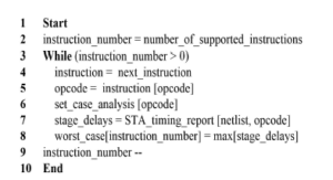
Figure 1: The proposed timing analysis methodology which studies each instruction as an individual entity.
In the sequel, we keep record of the slowest pipeline stage timing, before moving on to the next instruction. Finally we pick another instruction and reiterate this process, until all the available instructions are exhausted.
It becomes clear that the proposed timing analysis methodology is a hybrid between STA and DTA. In this sense, it performs STA for each instruction of the processor ISA, but it further analyzes all possible instructions, giving a DTA flavor to the result. However, it is not a full DTA, since it only varies the opcode field of the instruction word, thus not considering input values neither for any other field of the instruction word nor for any other part of the circuit. In particular, the implementation of the architecture we work on supports 215 instructions, which means that we only need 215 analyses in our method, instead of 264 which would be needed for a full DTA on the variations of the instruction word alone, or many more if we were to consider other circuit inputs as well. On the other hand, our approach is not as pessimistic as classic STA, and with only little higher complexity it can produce designs that exhibit significantly better performance than designs produced by STA. Our second approach presented next can produce even more efficient designs.
3.3 Dynamic Opcode Value Changes
Using the proposed technique we manage to analyze the timing requirements of each processor instruction individually. To this end, we are iteratively affixing certain circuit inputs at constant voltage values. Specifically, we are bounding the opcode field bits to static binary values in order to analyze each instruction behavior.
In real time digital circuits, inputs change in a dynamic way as new values are stored into the pipeline registers at the rising edge of the clock signal, immediately before they are needed and used. As a result, new instructions are fetched for execution on each clock cycle and thus, inputs representing the opcode bits of each instruction are not constrained to fixed voltage values; instead they dynamically change, resulting in an unpredictable transient timing behavior in every pipeline stage after the fetch stage. Such behavior appears at the decode stage due to the opcode bits per se, as well as at all subsequent stages due to the control bits produced by the opcode bits and is propagated to such stages. For this reason, the discrepancy between our initial concept and a real time system behavior in timing deviations should be addressed.
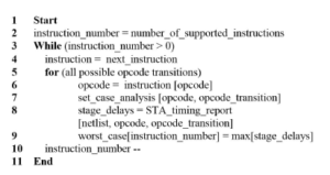
Figure 2: The timing analysis methodology which compensates for the dynamic voltage change of the opcode field.
In order to compensate for the dynamic voltage change in the processor pipeline inputs, we employ a modification of the aforementioned timing analysis methodology. Since our focus is now around the timing variance created by the dynamic behavior of the instruction opcode field, we consider the opcode as a bit sequence whose length is defined by the ISA. Consequently we have to take into account every possible value transition which leads to the currently analyzed bit sequence. Normally the amount of all possible combinations grows exponentially with the length of the sequence. We consider this approach unsuitable for our needs as its high time cost makes it impossible for practical application. Furthermore, we aim at the development of a methodology, which can be employed to analyze any ISA, without depending on the instruction opcode length of the design.
The solution we propose to resolve this is based on the observation that in processor architectures not all possible bit transitions lead to valid bit sequences of the opcode field. More specifically, as the instructions succeed one another during the instruction fetch stage, the number of valid opcode bit combinations is constrained by the number of the instructions supported by the ISA. So instead of analyzing the timing delay of each possible opcode bit sequence transition, we focus on the analysis of each possible instruction succession.
Figure 2 depicts the proposed solution, which relies on the initial concept as described earlier, augmented with the dynamic value change compensation approach we discussed. In this solution, we analyze each instruction’s timing requirements individually as before, but instead of using fixed voltage values to describe the currently examined instruction, we analyze each possible opcode transition that could lead to the opcode bits of the current instruction. Such transitions represent any rising and falling voltage values that could result in that particular bit sequence. The timing analysis of such cases is studied individually, while the timing analysis tool propagates all generated signals through the processor pipeline. We still use the “case analysis” function, as it can be expanded to include rising and falling voltage change. When we complete the timing analysis of an instruction, we save the worst-case delay. Afterwards we proceed with the analysis of the next instruction, until all supported instructions are exhausted.
The method we proposed in this section uses STA to find the worst-case delay path of each individual instruction. But in order to achieve an accurate timing result we utilize an exhaustive iterative analysis resembling more now that of a DTA method. However, even if we restrict value variations within the instruction opcode, with an opcode field of x bits, a standard DTA approach would require 2x iterative timing analyses to effectively analyze the timing of the opcode length, as each possible x-bit combination may lead to the required sequence. Instead, using our methodology, the number of iterations needed for each opcode analysis is only equal to the total number of supported instructions, in our case 215 iterations.
The proposed timing analysis technique lies somewhere between STA and DTA, closer to STA with respect to complexity, but closer to DTA with respect to output quality. We call this technique Pseudo Dynamic Timing Analysis (PDTA). In the following section we discuss the application of PDTA to adaptively scale the clock frequency of the core pipeline of a processor.
4. Clock scaling using opcode-based pseudo dynamic timing analysis
4.1 Adaptive clock scaling in pipelined processors
Adaptive clock scaling is often used for power control in modern high-performance processor architectures. Processor cores can be slowed down when not in full use, in an attempt to reduce power consumption and avoid overheating. In some cases, cores can be sped up for a limited time, in order to boost performance for cyclehungry applications. On the other hand, low-cost processors that are preferred for embedded and low-performance systems can also use clock scaling in order to increase performance, especially if this is achieved in a fairly cheap manner.
Another way to effectively scale up the clock frequency is to deepen the processor pipeline. In this way each stage’s latency is reduced and the system may operate lower clock periods. Previous works in [30] and [31] demonstrate that deepening the processor pipeline results in an increase in circuit area and power consumption due to the implementation of additional pipeline registers, Furthermore, deep pipelined processors require more complicated forwarding, control and stalling mechanisms thus, further impairing the design’s area and power requirements. As a result, authors in [30] and [31] conclude that the increase of the pipeline stage amount does not necessarily result in performance increase as the costs of wrong branch predictions and pipeline flushing become greater.
Our work focuses on low-cost IoT processors which present significantly low area and power requirements as stated in [32], [33]. Under this premise we do not opt in deepening the pipeline width or enhancing the complexity of the system, instead we focus on increasing the processor throughput while preserving the system microarchitecture as it is. In this section we will present how PDTA can be employed for such a purpose.
4.2 Scaling clock by opcodes
PDTA can be used to acquire timing information for each instruction separately and thus, we aim to use such information for adaptive clock scaling based on the instruction opcode. In order to validate our clock-scaling technique, we will continue using the same 64-bit six-stage pipelined processor that we referred to in Section 3, which is a single-issue in-order-execute RISC-V processor implementation.
We will refer to this implementation as “baseline processor”. In order to tighten the timing of the processor’s functional units we also deploy a second implementation that utilizes pipelined functional units. As a result time consuming operations require more clock cycle to complete but they display lower latency. We will refer to this implementation as “pipelined execution”. We classify the obtained results into 11 instruction classes as shown in Table 1. Each instruction class contains a group of individual instructions with similar timing requirements. We also pinpoint the slowest pipeline stage in terms of delay, for every class and we refer to such stage as “critical stage”. Finally, we assign a “worst-case delay” value to each class, which is the highest instruction delay in the corresponding group. The classes go as follows:
- The Logical instruction class which includes logical operations such as and, ori and xor.
- The Shift instruction class which includes shift operations such as shift left logical or shift arithmetic.
- The Comparison instruction class which includes bit comparison
- The Jump instruction class which includes jump operations such as jump and link, jump register or jump.
- The Multiplication instruction class which includes integer multiplication
- The Division instruction class which includes any integer division
- The Other arithmetic instruction class which includes all other integer arithmetic operations except for multiplication and division, such as addition or subtraction.
- The Memory access instruction class which includes any memory access operation such as load word or store byte.
- The FP Multiplication instruction class which includes floating point multiplication
- The FP Division instruction class which includes floating point division
- The Other FP arithmetic instruction class which includes all other floating point arithmetic operations except for FP multiplication and division, such as FP addition or subtraction.
Table 1: Analysis of the instruction classes of the RiscV Rocket core architecture.
| Instruction class | Slowest pipeline | Baseline worst | Pipelined execution |
| stage (critical stage) | case delay | worst case delay | |
| Logical | Execute stage | 1.2 ns | 1.2 ns |
| Shift | Execute stage | 1.5 ns | 1.5 ns |
| Comparison | Execute stage | 1.5 ns | 1.5 ns |
| Jump | Execute stage | 1.1 ns | 1.1 ns |
| Multiplication | Execute stage | 2.9 ns | 1.5 ns |
| Division | Execute stage | 3.3 ns | 1.1 ns |
| Other arithmetic | Execute stage | 1.9 ns | 1 ns |
| Memory access | Memory stage | 3.9 ns | 1.3 ns |
| FP Division | Execute stage | 3.7 ns | 1.3 ns |
| FP multiplication | Execute stage | 3.2 ns | 1.1 ns |
| Other FP arithmetic | Execute stage | 3.0 ns | 1 ns |
After studying the aforementioned instruction classes we observe the following:
- Each pipeline stage presents unique timing requirements depending on the instruction being executed.
- Some pipeline stages may produce error free results while utilizing higher clock frequencies than the others.
- The error free instruction execution is preserved if we satisfy the timing requirements of each individual pipeline stage for the executing instruction.
We deduce that we can dynamically adapt the clock period of the processor during the run time in order to achieve higher throughput, while also guarantying the error free instruction execution. To this end, we isolate the critical instructions, i.e. the instructions that constrain the clock frequency and we display the results we obtained for each implementation in Table 2. We track down all critical instruction classes for our architecture and we assign a minimum operational clock period to each one of them. Due to the prior timing analysis, we are guaranteed that each critical instruction will execute without errors at the designated clock period. We also consider a typical clock period for each design which is suitable for the error free execution of non-critical instructions.
Our design focuses on letting the pipeline operate at high clock frequencies when critical instructions are absent. When a critical instruction is detected, we downscale the clock frequency, as soon as the critical instruction enters the pipeline stage which would otherwise cause a timing error. We refer to such stage as critical stage. Figure 3 shows an execution instance of a small instruction sequence on the Rocket core Baseline implementation. We track the minimum clock period with respect to the pipeline stages involved and we mark the critical stages that contribute to frequency downscaling. Under this premise, the critical stage is the slowest pipeline stage in which the clock frequency needs to be adjusted so that no timing errors to occur. In this example, the pipeline under examination may operate at higher clock frequencies during the 1st to 5th and 8th to 10th clock cycle, while the clock frequency must be lower at the 6th and 7th cycle.
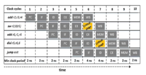
Figure 3: An instruction execution instance of the Rocket core implementation displaying the minimum operational clock period during each stage.
Table 2: The clock periods for critical instructions along with the typical clock period for the Rocket core implementation.
RiscV baseline RiscV pipelined execution
Multiplication, Division, Shift, Comparison,
Critical instruction class Memory access, FP division, Multiplication FP multiplication
Critical instruction clock 4 ns 1.5ns
Typical clock 2 ns 1.3 ns
4.3 Dynamic clock scaling mechanism
We will now present in detail the circuit we designed to enforce the adaptive selection of the clock frequency. The circuit uses the information extracted from the timing analysis proposed in Section 3, to designate whether the clock frequency should be adapted. As the decision making will be occurring in real time, our design needs to employ reliability and speed. Figure 4 displays the designed clock control unit, which is charged with such task, and is implemented on the Rocket core implementation. It consists of an instruction snooping module and a clock selection module. In order to make the design nonintrusive for the processor architecture, we attach the two-module circuit at the side of the fetch and the decode stages of the processor pipeline.
Instruction snooping module: To be able to change the clock frequency dynamically, we need information about the class of the instructions that are headed for execution. To this end, we implement an instruction snooping circuit that receives a copy of the instruction word coming out of the instruction cache. This circuit monitors the instructions fetched and tracks down their progress in the pipeline. Moreover, it utilizes lookup tables which contain both the critical instruction opcodes and the critical pipeline stage for each corresponding instruction as calculated in Section 4.2. Using this information, the circuit produces a logical output on whether the clock frequency must be changed, driving with that output the clock selection module. Clock selection module: This module propagates the appropriate clock pulse selected by the frequency selector mechanism of the instruction snooping module. The clock selection module inputs are the frequency selection signal generated by the instruction snooping module and two PLL signals, one of high and one of low frequency. The frequency selection signal determines which pulse will be selected for the pipeline clock, when the instruction arrives at the critical stage. If frequency is indeed switched to low, the module must revert to the high frequency in the following cycle. The selection circuit is a simple multiplexor with insignificant contribution to the total delay of the module.
In the implementation of the second module, we observed that reverting to the original frequency may result in an unstable pipeline clock behavior, as shown in Figure 5. Such a phenomenon exists due to the frequency difference between the clocks and may prove catastrophic for the instruction execution. We address this problem in the way shown in Figure 6, by generating another low frequency pulse signal with a 180 degrees phase shift of the original. We also design a phase selector circuit which is responsible for selecting the appropriate phase when necessary. The phase selector is signaled by the frequency selector when a frequency scaling event is about to happen. It then designates the selected PLL phase so that no unstable behavior is exhibited. The complexity of the phase selection mechanism depends on the number of PLLs required.
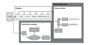
Figure 4: The clock control unit integrated in the rocket core.
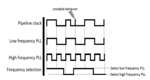
Figure 5: Unstable clock behavior due to subsequent clock selections.
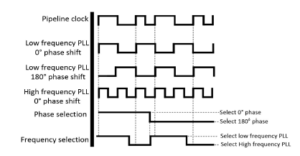
Figure 6: The clock instability compensation technique.
In the case of the implemented Baseline RiscV pipeline, where one period is an integer multiple of the other (2ns and 4ns), the generation of one additional shifted PLL resolves the problem. In other processor implementations though, additional PLLs may be needed, each with a specific phase shift, in order to enable the phase selector to compensate for all possible unstable behaviors of the pipeline clock. We adopt this approach as we acknowledge the need for a robust real time clock scaling mechanism. In contrast with [19] and [20] which manage to change the clock frequency for up to 7.5% of the core clock speed, we require much higher adaptation values. For that reason we do not change the clock frequency directly, instead we pre-generate the number of PLLs required and we proceed in selecting the appropriate candidate each time.
In general, when we have two clocks with a period ratio m:n, m and n being mutually primes, we need m PLLs for the phase shifts of the first and n PLLs for the phase shifts of the second clock, giving a total of m+n PLLs. Such a solution to the possible instability problem serves as the most efficient in terms of performance. As we saw earlier, clock frequencies used are the highest possible, with longer clock periods just enough to cover the critical pipeline stage delay. But this choice may result in a large number of PLLs. A cheaper solution would be to always use a slow clock period that is a multiple of the typical period. In this way we would not need that many PLLs, sacrificing performance for simpler implementation. In some cases, like the one examined above, it occurs that the optimal performance solution coincides with the cheapest solution, but this is definitely not the general case though.
4.4 Clock tree synthesis and distribution network
The proposed methodology requires the adoption of multiple PLLs to formulate the processor core clock frequency. The processor clock is dynamically selected according to the information obtained by the clock control unit and any change should be enforced within a very limited amount of time. Previous works in [21] and [15] have shown that cycle-to-cycle clock selection is possible and thus, the feasibility of the proposed methodology is ensured. To this end we opt to synthesize a single clock tree that reaches every register of the design, as we consider the propagation of all the available PLLs very costly. Under this premise, we perform the clock tree synthesis operation as if the design was operating under a single core clock with a constant clock frequency. The resulting clock distribution network is implemented by using timing constrains for the lower possible period that is obtainable by the clock in our designs, i.e. 2 ns and 1.3 ns for the corresponding “baseline” and “pipelined execution“ implementations.
The clock control logic is implemented in a global level; on the clock tree root where the available PLLs are driven in order to select the most appropriate to propagate through the constructed clock tree.
In this way we avoid the expensive area, routing and energy costs of multiple PLL distribution, but we impose timing skew in the clock tree network. Also local, cell level clock gating for heavily gated clock networks such as ours results comes with various challenges, as a previous works in [34] and [35] suggest, that are not within the scope of this work.
In order to compensate for such a delay we design the clock selection unit to generate the outputs that control the clock selection process within the available timing margins. In this sense, we implement a low complexity and low latency control circuit capable of generating outputs with low delay, before the imminent clock pulse. As a result each decision on the dynamic clock frequency change is made within the timing margin available in order to properly distribute the clock pulse throughout the clock network in time. Also, the clock tree synthesis process we employ does not require the routing of all the PLLs of the design; instead it manages to propagate the dynamically selected PLL through a single synthesized clock tree.
5. Evaluation
In this section we discuss the evaluation process we employ in order to evaluate the PDTA methodology. To this end, we elaborate on the CAD toolflow and simulation environment we utilize and we present the results we obtain in terms of speedup, power consumption and overhead of the PDTA.
5.1 CAD toolflow and simulation
After rigorous consideration of many open-source simple processor cores that have been used in architecture-oriented research in the last decade, we have opted for the RiscV Rocket Core [36] processor implemented in Verilog for evaluating our methodology. We have implemented two processor versions as mentioned in Section 4, both of which include our clock control design; we then compiled and tested the circuits using a number of benchmarks, and produced a final evaluation of our ideas. For the front-end design flow we used the Synopsys Design Compiler [37] in conjunction with the NanGate
45nm Open Cell Library [38], whereas for the back-end place and route process we used the Synopys IC Compiler [39]. Afterwards, we used Synopsys PrimeTime [40] to apply the PDTA methodology we described in Section 3 on the generated post-placement netlists. We subsequently performed post-layout simulations, back annotating the design with Mentor Graphics Modelsim [41]. In order to analyze the performance and power consumption of the system, we selected the SPEC CPU2017 benchmark suite and we utilized the RiscV toolchain to compile each benchmark to generate the required binaries in accordance with the RiscV architecture. Finally, we employed Synopsys Power Compiler [42] to generate power reports for each benchmark. The parameters of both the baseline processor and the pipelined execution implementations are displayed in Figure 7. The processor supports in-order instruction issue and execution with 64-bit instruction length. It also employs a BTB of 512 entries using the g-share prediction mechanism. We have also incorporated an L1 cache to the processor; in particular a 4-way associative 16KB i-cache and a 4-way set associative 16KB
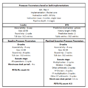
Figure 7: The configuration parameters of both processor implementations.
d-cache with LRU replacement policy. The access time of the data cache is 4 and 7 clock cycles for the baseline and the pipelined execution implementations correspondingly, while the access time for the instruction cache is 1 clock cycle. The clock period for each implementation is defined by the slowest pipeline stage as described in section 4. Finally, the amount of PLLs required for the implementation of the PDTA methodology is 4 for the baseline and 18 for the pipelined execution RiscV implementations.
5.2 Speedup
We have run the Spec2017 CPU benchmarks on the baseline processor implementation, on the pipelined execution implementation and on their corresponding BTWC versions. We present the normalized instruction throughput improvements we obtained according to our experiments in Figure 8 where results indicate an average performance increase in instruction throughput of 1.6 and 1.3 correspondingly. In the same figure we also present the appearance rate of critical instructions for each processor implementation. Further result analysis discloses the following information:
Firstly, designs with relaxed timing constrains benefit more from the PDTA methodology when compared with designs that display tighter timing requirements. This behavior is expected as the PDTA methodology exploits timing differences between individual processor operations. As a result, the more relaxed the system timing, the higher performance increase is achieved. Secondly, frequent appearance of critical instructions throttles the system’s performance as the design is forced to operate under the worst-case clock period. As a result benchmarks that display low critical instruction appearance rates, also display higher throughput increase.
In order to further assess the effectiveness of PDTA methodology we compare the obtained throughput results with other state of the art timing speculation techniques. Tables 3 and 4 below demonstrate processors.
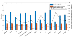
Figure 8: Normalized throughput improvement and critical instruction appearance rate of the proposed design methodology compared to the corresponding baseline
the outcomes of such comparison. Table 3 depicts the normalized throughput improvement of the application-adaptive guardbanding technique proposed by A. Rahimi et. Al. in [10]. We compare the PDTA methodology of both RiscV implementations with the best and worst performance-wise design corners explored by [10]. The application-adaptive guardbanding technique outperforms our methodology when it comes to the best-case design corners, but PDTA proves to be more efferent in terms of performance in worstcase design corners. Table 4 below displays the PDTA results in conjunction with Blueshift optimization as described in [15]. In this work the proposed TS methodology is applied on both Razor [4] and OpenSPARC T1 processors displaying significant performance improvements. According to table 4 PDTA design approach achieves better throughput improvements if compared with Razor or OpenSPARC T1 processor when the baseline RiscV is considered. In contrast, the pipelined execution RiscV design is slightly behind the Razor processor in terms of performance, while it still surpasses the OpenSPARC T1 with the Blueshift design paradigm. PDTA comparison with state of the art TS methodologies highlights the competitive edge of our methodology as its performance is measured on average the same level if not above, compared to other TS approaches.
Table 3: Throughput improvement comparison between Application-adaptive guardbanding and PDTA.
Adaptive Guardbanding PDTA Baseline
Benchmark Best/Worst design /PDTA Pipelined
corner [10]
djikstra 1.87 / 1.36 1.61 / 1.28 patricia 1.89 / 1.38 1.8 / 1.26 susan 1.81 / 1.58 1.4 / 1.25 blowfish 1.84 / 1.35 1.6 / 1.25 Average 1.88 / 1.25 1.6 / 1.26
Table 4: Throughput improvement comparison between Blueshift OpenSPARC, Razor and PDTA methodology.
| b2zip | 1.18 | 1.37 | 1.8 / 1.28 |
| gcc | 1.25 | 1.39 | 1.42 / 1.29 |
| mcf | 1.04 | 1.05 | 1.7 / 1.25 |
| Average | 1.15 | 1.27 | 1.64 / 1.273 |
5.3 Power consumption compared to the baseline processor
Due to clock frequency scaling, our design often tends to operate at higher frequencies. As higher frequencies are more power hungry, we expect a higher power usage compared to the baseline processor. To verify that assumption, we measure the power consumption of the BTWC design and we compare it to its relevant baseline processors in Figure 9. Results show that the power consumption increase is higher for the benchmarks that present more opportunities for aggressive frequency scaling. Specifically, an increase of 4% to 36% in power consumption is observed, depending on each benchmark’s capacity for frequency scaling. Nevertheless, by dividing the performance improvement over the power increase for each benchmark, we get an average of 3.7 improvement rate for the performance-to-power ratio, which is a quite significant overall improvement that we observe with our technique.
5.4 Overhead of the PDTA methodology
In order to properly evaluate the overhead of the PDTA methodology we measure both the PDTA design costs in terms of area and power complexity and the PDTA analysis cost in terms of time requirements.
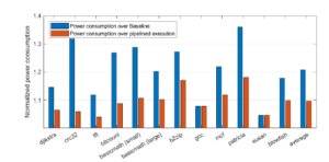
Figure 9: Normalized power consumption increase of the proposed methodology compared to the baseline processors.
Regarding the design costs of the PDTA, we quantify the overhead in power and area of the post-layout implementation of the clock control circuit and instruction snooping modules. Such modules are the essential components of the PDTA design and are used as described in section 4. Table 5 lists the power and area requirements of the aforementioned modules, along with the power and area requirements of the baseline processors. We observe that the power overhead of the control unit is less than 2% of the total average power consumption of the baseline pipelines, while the area overhead almost 0.001%. Further, Table 6 depicts the area overhead comparison between the state of the art methodologies and the PDTA approach which is proposed in this work. We observe that the PDTA methodology achieves the least area overhead compared with the rest and thus, we conclude that the PDTA is well suited for low-end, low power pipelined processors.
Regarding the time requirements of the PDTA, we measure the amount of iterations and the amount of time required for the PDTA analysis to complete. The results we obtain are depicted in Table 7 in comparison with the standard STA and DTA methodologies. We define the iteration count as the amount of times the corresponding timing methodology in invoked in order to sufficiently cover the timing paths of the pipeline under examination. To this end, the DTA methodology examines every possible bit-transition and thus, it requires 2instruction length iterations (264 for the 64-bit RiscV Rocket core implementations). On the other hand, the STA methodology examines the worst case scenario only, for each instruction path and thus, the required timing iterations are analogous to the complexity of the design. The PDTA methodology resides in between the DTA and STA approaches as the amount of the required iterations is depended on the bit length of the opcode field of the ISA, as discussed in section 3. As a result, the PDTA requires 27 iterations in order to properly analyze the timing paths of the RiscV Rocket core pipeline, as the opcode field of the rocket core ISA is 7 bits. In order to evaluate the time requirements of each methodology, we run the DTA, STA and PDTA approaches on the same RiscV rocket core pipeline using an Intel i7 coffee lake processor with 6 cores and 16 GB of DDR4 DRAM. Results indicate that the STA analysis finishes in a 20 second period of time while the PDTA methodology requires 5 minutes. In contrast, the DTA requires over 100 hours to finish and thus, it is considered time costly for timing analysis in processor pipelines. We conclude that the PDTA methodology manages to efficiently manage the tradeoffs between STA and DTA as it provides detailed timing reports for each ISA-supported instruction while also requiring a reasonable time to finish.
Table 5: The power and area overhead of the clock control and instruction snooping circuits in comparison to RiscV .
| Implementation | Average power | Area |
| RiscV Baseline | 65.67mW | 0.24mm2 |
| RiscV Pipelined execution | 149.04mW | 0.55mm2 |
| Clock control and instruction snooping | 98.21uW | 321um2 |
Table 6: Area overhead comparison between PDTA methodology and the state of the art.
| iRazor [5] | 13.6% |
| Application-adaptive guardbanding [10] | 0.022% |
| TS Cache [17] | 1.8% |
| Active management [18] | 0.12% |
| DynOR [21] | 5 − 13% |
| Optimal In Situ Monitoring [26] | 3.15% |
| Razor-Lite [43] | 4.42% |
| Bubble Razor [44] | 21% |
| PDTA (this work) | 0.001% |
Table 7: Time requirements of DTA, STA and PDTA to complete the timing analysis of RiscV pipeline.
| Implementation | Iterations | Iterations | Time |
| Theoretical | (RiscV) | (RiscV) | |
| DTA | 2instruction length | 264 | Over 100 hours |
| STA | Supported instructions | 215 | 20 seconds |
| PDTA (this work) | 2opcode length | 27 | 5 minutes |
5.5 PVT tolerance considerations
In order to evaluate our design we utilize a single design corner that operates in 0°and 0.72 V. We select the aforementioned corner as the 0.72 V is considered low power pipeline operation and thus, it stays within the scope of this work. We also set a clock uncertainty of 10% to compensate for the process variation effect which may induce clock jitter and uncertainty to the integrated circuit. Evaluating the proposed methodology with a full range of dynamic variations as well as static process parameters variations is possible but the PDTA analysis should be conducted independently for each individual design corner. A higher voltage than 0.72 volts would result in shorter delay instruction paths, while lower operating temperatures would lead to higher delays in the low-voltage region of 0.72 volts as previous work in [45] demonstrates. To this end, the PDTA analysis should be conducted for each design corner in order to extract the exact timing information for the corresponding operating Voltage and Temperature values. On the other hand, the process variation effect can be emulated by setting clock jitter and clock delay values, similarly to our approach. The methodology of the PDTA does not require any modifications in order to function properly within different PVT effects and thus, it can produce accurate timing results given the exact operating condition of the integrated circuit.
6. Conclusion
The BTWC design paradigm promises to alleviate critical path constraints which have negative effects on processor timing. In this paper we present PDTA, a timing analysis methodology, which shifts the focus from a general critical path analysis to the less constrained analysis of paths that are actually followed by individual instructions. To this end we design and implement a circuit capable of identifying the timing requirements of any incoming instruction and selecting the appropriate pipeline clock out of a number of deployed PLLs. Thus we are able to scale up the clock frequency beyond its worst-case operational limit. We evaluate our methodology using a RiscV processor architecture which presents differences in pipeline stage timing. Results demonstrate an average performance increase of 1.62x, as well as a 3 to 4-fold improvement in performance-to-power ratio, compared to the baseline processor. The main contributions of this work to the current state of the art include:
- We propose a novel methodology implemented on the circuit level which considers instruction opcodes for performance increase. Previous consideration of opcodes for performance increase has been compiler-only consideration, i.e. instructions with expensive opcodes are identified at compile time and avoided in code generation.
- The timing analysis we present is focused on individual instructions rather than on whole instruction sequences. In this way we collect information that is more applicable in real systems, as certain instruction sequences do not appear in a steady and predictable rate.
- Our methodology identifies the timing requirements of individual incoming instructions. Since we are a priori aware of such constraints, we do not deploy any error detection or error correction mechanism, while also avoiding any metastable behavior which commonly manifests in such cases. • We explore an architecture-oriented approach for the BTWC design paradigm. Our work studies the processor architecture to extract timing information based on the ISA of the processor. As a result, we consider this approach to have greater applicability as it can be used on any processor architecture without requiring any further adjustments. • The proposed methodology does not make any intrusive changes on the processor architecture. This means that it can be applied without any additional design costs, and it maintains the original pipeline intact.
Overall, the BTWC approach presents many opportunities for designers to experiment with novel methodologies and innovative techniques. We believe that research will produce various studies related to this field in the future, as it promises to redefine the design paradigm of modern integrated circuits. Finally, given the dominance of low-cost processors in embedded and many domainspecific designs, ideas that boost performance of processors within those fields in a simple and cheap way will appear, some of which successfully establishing new directions in microprocessor design.
Conflict of Interest
The authors declare no conflict of interest.
- A. Tziouvaras, G. Dimitriou, M. Dossis, G. Stamoulis, “Adaptive Operation- Based ALU and FPU Clocking,” in 2020 9th International Conference on Modern Circuits and Systems Technologies (MOCAST), 1–4, 2020, doi: 10.1109/MOCAST49295.2020.9200282.
- T. Austin, V. Bertacco, “Deployment of better than worst-case design: solutions and needs,” in 2005 International Conference on Computer Design, 550–555, 2005, doi:10.1109/ICCD.2005.43.
- R. Ye, F. Yuan, J. Zhang, Q. Xu, “On the premises and prospects of timing speculation,” in 2015 Design, Automation Test in Europe Conference Exhibition (DATE), 605–608, 2015, doi:10.5555/2755753.2755890.
- D. Ernst, Nam Sung Kim, S. Das, S. Pant, R. Rao, Toan Pham, C. Ziesler, D. Blaauw, T. Austin, K. Flautner, T. Mudge, “Razor: a low-power pipeline based on circuit-level timing speculation,” in Proceedings. 36th Annual IEEE/ACM International Symposium on Microarchitecture, 2003. MICRO-36., 7–18, 2003, doi:10.1109/MICRO.2003.1253179.
- Y. Zhang, M. Khayatzadeh, K. Yang, M. Saligane, N. Pinckney, M. Alioto, D. Blaauw, D. Sylvester, “iRazor: Current-Based Error Detection and Correction Scheme for PVT Variation in 40-nm ARM Cortex-R4 Processor,” IEEE Journal of Solid-State Circuits, 53(2), 619–631, 2018, doi:10.1109/JSSC.2017.2749423.
- V. Subramanian, M. Bezdek, N. D. Avirneni, A. Somani, “Superscalar Processor Performance Enhancement through Reliable Dynamic Clock Frequency Tuning,” in 37th Annual IEEE/IFIP International Conference on Dependable Systems and Networks (DSN’07), 196–205, 2007, doi:10.1109/DSN.2007.90.
- T. Austin, V. Bertacco, D. Blaauw, T. Mudge, “Opportunities and challenges for better than worst-case design,” in Proceedings of the ASP-DAC 2005. Asia and South Pacific Design Automation Conference, 2005., I/2–I/7 Vol. 1, 2005, doi:10.1109/ASPDAC.2005.1466113.
- C. C. Wang, K. Y. Chao, S. Sampath, P. Suresh, “Anti-PVT-Variation Low- Power Time-to-Digital Converter Design Using 90-nm CMOS Process,” IEEE Transactions on Very Large Scale Integration (VLSI) Systems, 28(9), 2069– 2073, 2020, doi:10.1109/TVLSI.2020.3008424.
- B. Poudel, A. Munir, “Design and Evaluation of a PVT Variation-Resistant TRNG Circuit,” in 2018 IEEE 36th International Conference on Computer Design (ICCD), 514–521, 2018, doi:10.1109/ICCD.2018.00083.
- A. Rahimi, L. Benini, R. K. Gupta, “Application-Adaptive Guardbanding to Mitigate Static and Dynamic Variability,” IEEE Transactions on Computers, 63(9), 2160–2173, 2014, doi:10.1109/TC.2013.72.
- T. Abhishek, S. Smruti R., T. Josep, “ReCycle: Pipeline Adaptation to Tolerate Process Variation,” in Proceedings of the 34th Annual International Symposium on Computer Architecture, ISCA ’07, 323–334, Association for Computing Machinery, New York, NY, USA, 2007, doi:10.1145/1250662.1250703.
- S. Sarangi, B. Greskamp, A. Tiwari, J. Torrellas, “EVAL: Utilizing processors with variation-induced timing errors,” in 2008 41st IEEE/ACM International Symposium on Microarchitecture, 423–434, 2008, doi:10.1109/MICRO.2008. 4771810.
- K. A. Bowman, J. W. Tschanz, S. L. Lu, P. A. Aseron, M. M. Khellah, A. Ray- chowdhury, B. M. Geuskens, C. Tokunaga, C. B. Wilkerson, T. Karnik, V. K. De, “A 45 nm Resilient Microprocessor Core for Dynamic Variation Tolerance,” IEEE Journal of Solid-State Circuits, 46(1), 194–208, 2011, doi: 10.1109/JSSC.2010.2089657.
- A. Omid, M. Aqeel, L. Benjamin C., P. Sanjay J., H. Mark, “Energy- Performance Tradeoffs in Processor Architecture and Circuit Design: A Marginal Cost Analysis,” in Proceedings of the 37th Annual International Symposium on Computer Architecture, ISCA ’10, 26–36, Association for Computing Machinery, New York, NY, USA, 2010, doi:10.1145/1815961.1815967.
- B. Greskamp, L. Wan, U. R. Karpuzcu, J. J. Cook, J. Torrellas, D. Chen, C. Zilles, “Blueshift: Designing processors for timing speculation from the ground up.” in 2009 IEEE 15th International Symposium on High-Performance Computer Architecture, 213–224, 2009, doi:10.1109/HPCA.2009.4798256.
- A. B. Kahng, S. Kang, R. Kumar, J. Sartori, “Designing a processor from the ground up to allow voltage/reliability tradeoffs,” in HPCA – 16 2010 The Sixteenth International Symposium on High-Performance Computer Architecture, 1–11, 2010, doi:10.1109/HPCA.2010.5416652.
- S. Shen, T. Shao, X. Shang, Y. Guo, M. Ling, J. Yang, L. Shi, “TS Cache: A Fast Cache With Timing-Speculation Mechanism Under Low Supply Voltages,” IEEE Transactions on Very Large Scale Integration (VLSI) Systems, 28(1), 252–262, 2020, doi:10.1109/TVLSI.2019.2935227.
- C. R. Lefurgy, A. J. Drake, M. S. Floyd, M. S. Allen-Ware, B. Brock, J. A. Tierno, J. B. Carter, “Active management of timing guardband to save energy in POWER7,” in 2011 44th Annual IEEE/ACM International Symposium on Microarchitecture (MICRO), 1–11, 2011, doi:10.1145/2155620.2155622.
- T. Hashimoto, Y. Kawabe, M. Kara, Y. Kakimura, K. Tajiri, S. Shirota, R. Nishiyama, H. Sakurai, H. Okano, Y. Tomita, S. Satoh, H. Yamashita, “An adaptive clocking control circuit with 7.5% frequency gain for SPARC processors,” in 2017 Symposium on VLSI Technology, C112–C113, 2017, doi:10.23919/VLSIT.2017.7998133.
- A. Grenat, S. Pant, R. Rachala, S. Naffziger, “5.6 Adaptive clocking system for improved power efficiency in a 28nm x86-64 microprocessor,” in 2014 IEEE International Solid-State Circuits Conference Digest of Technical Papers (ISSCC), 106–107, 2014, doi:10.1109/ISSCC.2014.6757358.
- J. Constantin, A. Bonetti, A. Teman, C. Mu¨ller, L. Schmid, A. Burg, “DynOR: A 32-bit microprocessor in 28 nm FD-SOI with cycle-by-cycle dynamic clock adjustment,” in ESSCIRC Conference 2016: 42nd European Solid-State Circuits Conference, 261–264, 2016, doi:10.1109/ESSCIRC.2016.7598292.
- S. Beer, M. Cannizzaro, J. Cortadella, R. Ginosar, L. Lavagno, “Metastability in Better-Than-Worst-Case Designs,” in 2014 20th IEEE International Symposium on Asynchronous Circuits and Systems, 101–102, 2014, doi: 10.1109/ASYNC.2014.21.
- K. A. Bowman, J. W. Tschanz, N. S. Kim, J. C. Lee, C. B. Wilkerson, S. L. Lu, T. Karnik, V. K. De, “Energy-Efficient and Metastability-Immune Resilient Cir- cuits for Dynamic Variation Tolerance,” IEEE Journal of Solid-State Circuits, 44(1), 49–63, 2009, doi:10.1109/JSSC.2008.2007148.
- X. Wang, W. H. Robinson, “Error Estimation and Error Reduction With Input- Vector Profiling for Timing Speculation in Digital Circuits,” IEEE Transactions on Computer-Aided Design of Integrated Circuits and Systems, 38(2), 385–389, 2019, doi:10.1109/TCAD.2018.2808240.
- Z. Li, T. Zhu, Z. Chen, J. Meng, X. Xiang, X. Yan, “Eliminating Timing Errors Through Collaborative Design to Maximize the Throughput,” IEEE Transactions on Very Large Scale Integration (VLSI) Systems, 25(2), 670–682, 2017, doi:10.1109/TVLSI.2016.2587810.
- H. Ahmadi Balef, H. Fatemi, K. Goossens, J. Pineda De Gyvez, “Timing Speculation With Optimal In Situ Monitoring Placement and Within-Cycle Error Prevention,” IEEE Transactions on Very Large Scale Integration (VLSI) Systems, 27(5), 1206–1217, 2019, doi:10.1109/TVLSI.2019.2895972.
- E. Tune, Dongning Liang, D. M. Tullsen, B. Calder, “Dynamic prediction of critical path instructions,” in Proceedings HPCA Seventh International Symposium on High-Performance Computer Architecture, 185–195, 2001, doi:10.1109/HPCA.2001.903262.
- J. Xin, R. Joseph, “Identifying and predicting timing-critical instructions to boost timing speculation,” in 2011 44th Annual IEEE/ACM International Symposium on Microarchitecture (MICRO), 128–139, 2011, doi: 10.1145/2155620.2155636.
- M. de Kruijf, S. Nomura, K. Sankaralingam, “A unified model for timing speculation: Evaluating the impact of technology scaling, CMOS design style, and fault recovery mechanism,” in 2010 IEEE/IFIP International Conference on Dependable Systems Networks (DSN), 487–496, 2010, doi: 10.1109/DSN.2010.5544278.
- H. Y. Cheah, S. A. Fahmy, N. Kapre, “Analysis and optimization of a deeply pipelined FPGA soft processor,” in 2014 International Conference on Field-Programmable Technology (FPT), 235–238, 2014, doi:10.1109/FPT.2014. 7082783.
- A. Hartstein, T. R. Puzak, “The optimum pipeline depth for a microprocessor,” in Proceedings 29th Annual International Symposium on Computer Architecture, 7–13, 2002, doi:10.1109/ISCA.2002.1003557.
- V. Agarwal, R. A. Patil, A. B. Patki, “Architectural Considerations for Next-Generation IoT Processors,” IEEE Systems Journal, 13(3), 2906–2917, 2019, doi:10.1109/JSYST.2018.2890571.
- B. M. Tariq, “A Study of Current Trends in the Design of Processors for the Internet of Things,” in Proceedings of the 2nd International Conference on Future Networks and Distributed Systems, ICFNDS ’18, Association for Computing Machinery, New York, NY, USA, 2018, doi:10.1145/3231053.3231074.
- L. Weicheng, S. Emre, S. Can, T. Baris, “Clock Skew Scheduling in the Presence of Heavily Gated Clock Networks,” in Proceedings of the 25th Edition on Great Lakes Symposium on VLSI, GLSVLSI ’15, 283–288, Association for Computing Machinery, New York, NY, USA, 2015, doi: 10.1145/2742060.2742092.
- C. Chang, S. Huang, Y. Ho, J. Lin, H. Wang, Y. Lu, “Type-matching clock tree for zero skew clock gating,” in 2008 45th ACM/IEEE Design Automation Conference, 714–719, 2008, doi:10.1145/1391469.1391653.
- K. Asanovic, R. Avizienis, J. Bachrach, S. Beamer, D. Biancolin, C. Celio, H. Cook, P. Dabbelt, J. Hauser, A. Izraelevitz, S. Karandikar, B. Keller, D. Kim, J. Koenig, Y. Lee, E. Love, M. Maas, A. Magyar, H. Mao, M. Moreto, A. Ou, D. Patterson, B. Richards, C. Schmidt, S. Twigg, H. Vo, A. Waterman, “The Rocket Chip Generator,” Technical report, EECS Department, University of California, Berkeley, April 2016.
- “Synopsys Design Compiler,” https://www.synopsys.com/ implementation-and-signoff/rtl-synthesis-test/design-compiler-graphical.html.
- C. H. M. Oliveira, M. T. Moreira, R. A. Guazzelli, N. L. V. Calazans, “ASCEnD- FreePDK45: An open-source standard cell library for asynchronous design,” in 2016 IEEE International Conference on Electronics, Circuits and Systems (ICECS), 652–655, 2016, doi:10.1109/ICECS.2016.7841286.
- “Synopsys IC Compiler,” https://www.synopsys.com/ implementation-and-signoff/physical-implementation/ic-compiler.html.
- “Synopsys PrimeTime,” https://www.synopsys.com/ implementation-and-signoff/signoff/primetime.html.
- “Mentor Graphics Modelsim,” https://www.mentor.com/products/fv/ modelsim/.
- “Synopsys Power Compiler,” https://www.synopsys.com/ implementation-and-signoff/rtl-synthesis-test/power-compiler.html.
- I. Kwon, S. Kim, D. Fick, M. Kim, Y. Chen, D. Sylvester, “Razor-Lite: A Light-Weight Register for Error Detection by Observing Virtual Supply Rails,” IEEE Journal of Solid-State Circuits, 49(9), 2054–2066, 2014, doi: 10.1109/JSSC.2014.2328658.
- M. Fojtik, D. Fick, Y. Kim, N. Pinckney, D. Harris, D. Blaauw, D. Sylvester, “Bubble Razor: An architecture-independent approach to timing-error detection and correction,” in 2012 IEEE International Solid-State Circuits Conference, 488–490, 2012, doi:10.1109/ISSCC.2012.6177103.
- R. Kumar, V. Kursun, “Reversed Temperature-Dependent Propagation Delay Characteristics in Nanometer CMOS Circuits,” IEEE Transactions on Circuits and Systems II: Express Briefs, 53(10), 1078–1082, 2006, doi: 10.1109/TCSII.2006.882218.