
Practical Simulation of Grounded/Floating Lossy Inductors Based on Commercially Available Integrated Circuit LT1228
Volume 6, Issue 2, Page No 512-520, 2021
Author’s Name: Tattaya Pukkalanun1, Pitchayanin Moonmuang1, Sumalee Unhavanich2, Worapong Tangsrirat1,a)
View Affiliations
1School of Engineering, King Mongkut’s Institute of Technology Ladkrabang (KMITL), Bangkok 10520, Thailand
2Faculty of Digital Technology, Chitralada Technology Institute, Bangkok 10300, Thailand
a)Author to whom correspondence should be addressed. E-mail: worapong.ta@kmitl.ac.th
Adv. Sci. Technol. Eng. Syst. J. 6(2), 512-520 (2021); ![]() DOI: 10.25046/aj060258
DOI: 10.25046/aj060258
Keywords: Commercially available IC LT1228, Inductance Simulator, Lossy Inductor

Export Citations
The article suggests four circuit topologies for the practical simulation of grounded and floating lossy inductors. All the suggested circuits use commercially available integrated circuit LT1228 chips as active elements, and only two passive elements, namely one resistor and one capacitor. The first two of the proposed circuits employ only a single LT1228 active element and can realize grounded lossy inductors without the need for element-matching conditions. The last two of the proposed circuits can realize synthetic floating lossy inductors with only two LT1228s. The values of simulated equivalent elements can be tuned electronically by simply adjusting the external DC bias current of the LT1228. Non-ideal transfer error effects of the LT1228 on the synthetic inductor performance are inspected. Sensitivity performance concerning transfer errors and active and passive elements is also demonstrated. PSPICE simulation results and experimental measurements of the commercially available integrated circuit, LT1228, are incorporated to corroborate all our theoretical analyses.
Received: 19 December 2020, Accepted: 28 February 2021, Published Online: 17 March 2021
1. Introduction
An inductance simulator circuit is an advantageous element in active circuit design and synthesis, especially for analog signal processing solutions and applications such as active filter, analog phase shifter, chaotic oscillator, and parasitic cancellation circuitry. In the past, there are various publications on the implementation of actively simulated lossy inductance simulators based on several active elements [1-34]. The first ones are intended for grounded lossy inductance simulation [1-22], while the others are for floating ones [23, 34]. However, from a careful inspection of the reported circuit topologies in these references, they have one or more of the following disadvantage features:
- The use of a relatively large number of active and passive electronic components for their constructions [2, 4-6, 20-21, 23-27, 30-32]. Although the circuits of [1, 7-19, 28-29, 33-34] employ only a single active component, they still require at least three passive elements. Owing to the employment of an excessive number of circuit components, these designs are not suitable for an integrated circuit (IC) implementation point of view.
- The lack of electronic tuning facility [1–2, 4, 6-18, 20-21, 24-31, 34].
- The need for strict component-matching conditions or cancellations for the grounded inductance function simulation [1, 6, 9].
- The use of different types of active electronic devices [20, 23-24, 32], which is inconvenient for further integrated circuit applications.
- The use of commercially unavailable ICs [1–3, 5-12, 15-17, 19-24, 26, 28-30, 32-34]. Also, the active building blocks used in these publications are complicated active functional blocks. Accordingly, the verification of the proposed realization is mostly performed by only computer simulation results.
Recently, several attempts have been proved that LT1228 IC package has now become a versatile and standard commercial IC in the realization of various types of analog signal processing applications [35-37]. This article reports the four circuit topologies for simulating all grounded/floating lossy inductors employing commercially available IC LT1228 chips as essential active components [38-39]. The first two circuit topologies ideally provide grounded lossy series and parallel inductors, while the other two topologies can emulate floating lossy series and parallel inductors. All the realized inductors employ canonical active and passive elements and are made adjustable electronically through the externally supplied current of the LT1228. The tracking error effects of the LT1228 on the circuit performance are investigated, and the active and passive sensitivity analyses are also evaluated. The validity of the synthetic lossy inductors is confirmed by the PSPICE simulation results using the macro-model of the LT1228 by Linear Technology as well as the prototype circuit test results using IC LT1228. Also, the circuit performance is demonstrated on an illustrative example of a voltage-mode second-order bandpass filter. The performance of the proposed practical grounded/floating lossy inductance simulators is compared with the previously presented similar works and also summarized in Table 1.
2. Characteristic of IC LT1228
Figure 1 shows the pin configuration and electrical symbol of the LT1228. It is a commercially available IC package, which is internally a combination of an operational transconductance amplifier (OTA) and a current feedback operational amplifier (CFA). The relationships between the appropriate terminal of LT1228 can be expressed through the following matrix expression given below [39]:
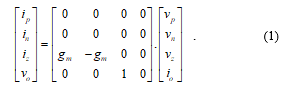 In matrix (1), gm is the transconductance gain of the LT1228, which is directly proportional to the external DC supplied current IB, as defined by the following relation [39]:
gm = 10IB. (2)
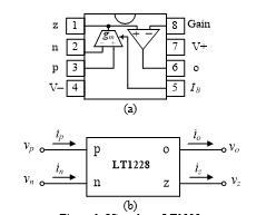 Figure 1: IC package LT1228
(a) internal active element and pin configuration (b) electrical symbol
3. Actively Realizable Lossy Inductance Simulator Circuits
Fig.2 shows the generic circuit configuration for the simulation of lossy grounded and floating inductors. They consist of IC package LT1228s as active elements. Routine analyses of the proposed circuits in Figure 2 yield the inductance functions and the finite quality factor (Q) given in Table 2. Inspection of the table, the four different inductance functions realized by the generic circuit topologies can be described in detail below.
- Figure 2(a) can emulate a grounded series RL-type lossy inductor with Req1 = 1/gm and Leq1 = R1C1/gm.
- Figure 2(b) can emulate a grounded parallel RL-type lossy inductor with Req2 = R2 and Leq2 = R2C2/gm.
- The circuit in Figure 2(c) can emulate a floating series RL-type lossy inductor with Req3 = 1/gm and Leq3 = R3C3/gm.
- The last circuit in Figure 2(d) can emulate a floating parallel RL-type lossy inductor with Req4 = 1/gm2 and Leq4 = C4/gm1gm2.
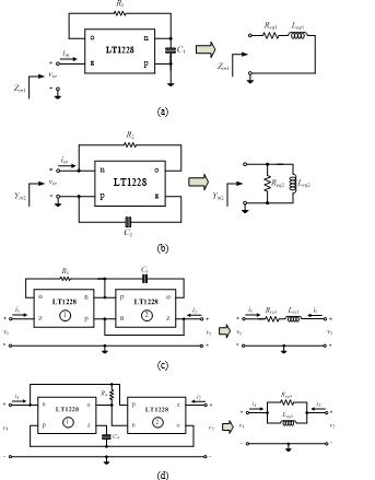 Figure 2: Lossy inductance simulators and equivalent circuits
(a) grounded series RL-type (b) grounded parallel RL-type
(c) floating series RL-type (d) floating parallel RL-type
Note that the proposed grounded lossy inductance sections of Figures 2(a) and 2(b) are no need for critical component-matching conditions. It is known that one can adjust the gm-parameter by changing the bias current of the LT1228, and then the simulated equivalent elements Req and Leq of the synthetic lossy inductors are electronically tunable.
Table 1: Performance comparison between the proposed lossy inductance simulators in Figure 2 and the previously published similar works
| Reference | Configuration | Inductor Type | Active device number | Passive device number | Commercially available IC | Matching condition | Electronic tuning | Technology | Supply voltage | Power dissipation | ||
| [1] | grounded | series, parallel | CCII = 1 | R = 4, C = 1 | no | yes | no | N/A | N/A | N/A | ||
| [2] | series, parallel | CCII = 3 | R ³ 2, C ³ 1 | no | no | no | AD844 | ±12V | N/A | |||
| [3] | parallel (Fig.3) | DO-VDBA = 2 | C = 1 | no | no | yes | N/A | N/A | N/A | |||
| [4] | series, parallel | CCII = 3 | R ³ 2, C ³ 1 | yes | no | no | AD844 | ±12V | N/A | |||
| [5] | series (Fig.3f) | EXCCTA = 2 | R = 2, C = 1 | no | no | yes | TSMC 0.18-µm CMOS | ±0.9V | N/A | |||
| parallel (Fig.3d) | ||||||||||||
| [6] | series (Fig.2) | CFOA = 2 | R = 3, C = 1 | no | yes | no | IBM 0.13-µm CMOS | ±0.75V (simulation), ±6V (experiment) | 3.53mW | |||
| [7] | series, parallel | CCIII = 1 | R = 2, C = 1 | no | no | no | B101 and B102 BJT | ±10V | N/A | |||
| [8] | series, parallel | CCIII = 1 | R = 2, C = 1 | no | no | no | TSMC 0.6-µm CMOS | ±2.5V | N/A | |||
| [9] | parallel (Fig.2c) | DXCCII = 1 | R = 2, C = 1 | no | yes | no | TSMC 0.35-µm CMOS | ±1.5V | N/A | |||
| [10] | series, parallel | DXCCII = 1 | R ³ 2, C = 1 | no | no | no | TSMC 0.35-µm CMOS | ±2.5V, +1.44V | N/A | |||
| [11] | series, parallel | DVCC = 1 | R = 2, C = 1 | no | no | no | MIETEC 0.5-µm CMOS | ±2.5V | N/A | |||
| [12] | series, parallel | OTRA = 1 | R ³ 2, C ³ 1 | no | no | no | MIETEC 1.2-µm CMOS | ±5V | N/A | |||
| [13] | series | CFOA = 1 | R = 2, C = 1 | yes | no | no | AD844 | ±15V | N/A | |||
| [14] | series | CFOA = 1 | R = 2, C = 1 | yes | no | no | AD844 | ±10V | N/A | |||
| [15] | series, parallel | CFOA = 1 | R = 2, C = 1 | no | no | no | IBM 0.13-µm CMOS | ±0.75V | 0.89mW | |||
| [16] | parallel | CDBA = 1 | R = 2, C = 1 | no | no | no | AD844 | ±12V | N/A | |||
| [17] | series (Fig.2e) | DXCCII = 1 | R = 2, C = 1 | no | no | no | TSMC 0.35-µm CMOS | ±1.5V | N/A | |||
| [18] | series (Fig.2d) | CFOA = 1 | R = 2, C = 2 | yes | no | no | AD844 | ±12V | N/A | |||
| [19] | series, parallel | FTFNTA = 1 | R = 1, C = 2 | no | no | yes | N/A | N/A | N/A | |||
| [20] | parallel (Fig.3) | VF = 1, CF = 1 | R = 3, C = 1 | no | no | no | 0.25-µm CMOS, AD844 | ±1.25V, +0.4V (simulation), ±12V (experiment) | 6.87mW | |||
| [21] | parallel (Fig.2a) | OTRA = 2 | R = 4, C = 1 | no | no | no | AD844 | ±10V | N/A | |||
| [22] | series (Fig.2c) | VDCC = 1 | R = 1, C = 1 | no | no | yes | TSMC 0.18-µm CMOS | ±0.9V | 0.87mW | |||
| [23] | floating | series (Fig.3) | CCCII+ = 2, CCCII- = 1 | C = 1 | no | no | yes | NR100&PR100 BJT,
AD844 |
±2.5V (simulation), ±5V (experiment) | 3.17mW | ||
| parallel (Fig.2) | CCCII- = 2 | C = 1 | ||||||||||
| [24] | series (Fig.2a) | DVCCS = 1, OA = 3 | R = 2, C = 1 | no | yes | no | N/A | N/A | N/A | |||
| series (Fig.2b) | DVCCS = 1, OA = 2 | |||||||||||
| parallel (Fig.2c) | DVCCS = 1, OA = 2 | |||||||||||
| [25] | parallel | CFOA = 2 | R = 3, C = 2 | yes | yes | no | AD844 | ±15V (experiment) | N/A | |||
| [26] | series, parallel | CCII = 2 | R = 2, C = 1 | no | no | no | N/A | N/A | N/A | |||
| [27] | series, parallel | CFOA = 2 | R = 2, C = 1 | yes | no | no | AD844 | N/A | N/A | |||
| [28] | series, parallel | DDCC = 1 | R = 2, C = 1 | no | yes | no | TSMC 0.18-µm CMOS | ±0.9V, +0.34V | N/A | |||
| [29] | parallel | DO-DDCC = 1 | R = 2, C = 1 | no | no | no | TSMC 0.35-µm CMOS | ±1.5V, -0.9V | N/A | |||
| [30] | series (Fig.2) | DDCC = 2 | R = 2, C = 1 | no | yes | no | IBM 0.13-µm CMOS | ±0.75V | 6.9mW | |||
| [31] | series, parallel | CFOA = 2 | R = 2, C = 1 | yes | no | no | AD844 | N/A | N/A | |||
| [32] | series (Fig.1) | DVB = 1, ECCII+ = 2, ECCII- = 1 | R = 3, C = 1 | no | no | yes | EL2082, AD830 | ±5V | N/A | |||
| [33] | parallel (Fig.4) | DDCC = 1 | R = 2, C = 1 | no | yes | no | IBM 0.13-µm CMOS, AD844 | ±0.75V | 2.08mW | |||
| [34] | series (Fig.2), parallel (Fig.3) | DDCC = 1 | R = 2, C = 1 | no | no | no | IBM 0.13-µm CMOS, AD844 | ±0.75V, +0.23V (simulation), ±9V (experiment) | 2.06mW | |||
| Proposed
circuits |
grounded | series (Fig.2a) | LT1228 = 1 | R = 1, C = 1 | yes | no | yes | LT1228 from Linear Technology Company | ±5V | 56.7mW | ||
| parallel (Fig.2b) | LT1228 = 1 | no | yes | 41.2mW | ||||||||
| floating | series (Fig.2c) | LT1228 = 2 | yes | yes | 0.114W | |||||||
| parallel (Fig.2d) | LT1228 = 2 | yes | yes | 0.117W | ||||||||
N/A : Not available
CCII : second-generation current conveyor, DO-VDBA : dual-output voltage-differencing buffered amplifier,
EXCCTA : extra X current conveyor transconductance amplifier, CFOA : current feedback operational amplifier, CCIII : third-generation current conveyor,
DXCCII : dual X second-generation current conveyor, DVCC : differential voltage current conveyor, OTRA : operational transresistance amplifier,
CDBA : current differencing buffered amplifier, FTFNTA : four terminal floating nullor transconductance amplifier,
VF : voltage follower, CF : current follower, VDCC : voltage differencing current conveyor, CCCII± : positive/negative current-controlled conveyor,
DVCCS : differential voltage controlled current source, OA : operational amplifier, DDCC : differential difference current conveyor,
DVB: differential voltage buffer, DO-DDCC : dual-output differential difference current conveyor,
ECCII± : positive/negative electronically controllable current conveyor
Table 2: Summary of the lossy inductance simulation using the proposed circuit configurations of Figure 2.
| Topology | Matching Condition | Realized inductance | Q |
| Figure 2(a) | no | wR1C1 | |
| Figure 2(b) | no | wC2/gm | |
| Figure 2(c) | gm = gm1 = gm2 | wR3C3 | |
| Figure 2(d) | R4 = 1/gm2 | wC4/gm1 |
4. Non-Ideal Consideration and Sensitivity Performance
If the non-ideal transfer errors are considered, the terminal relationships of the LT1228 can be described as follows:
 here, a = (1 – egm) and b = (1 – ev), where egm and ev are respectively the transconductance inaccuracy and the voltage transfer error in which |egm | << 1 and |ev | << 1. Re-analysis all the topologies in Figure 2 by taking the non-ideal parameters of the LT1228 into account, the various non-ideal characteristic parameters of the synthetic inductors can be evaluated and summarized in Table 3.
Table 3: Non-ideal parameters of the designed inductors in Figure 2.
| Topology | Simulated equivalent elements | Q | |
| Figure 2(a) | Req1 = 1/abgm | Leq1 = R1C1/abgm | wR1C1 |
| Figure 2(b) | Req2 = R2 | Leq2 = R2C2/abgm | wC2/abgm |
| Figure 2(c) | Req3 = 1/a1b1gm | Leq3 = R3C3/a1b1gm | wR3C3 |
| Figure 2(d) | Req4 = 1/gm2 | Leq4 = C4/a1b1gm1gm2 | wC4/a1b1gm1 |
Normalized sensitivities of the simulated equivalent values Req and Leq with respect to active and passive elements are obtained as:
 From the above, it is clearly seen that the magnitudes of these sensitivity coefficients are less than or equal to unity. Thus, it can be realized that all the proposed inductors exhibit good sensitivity performance.
5. Simulation Results
The proposed lossy inductance simulators in Figure 2 have been simulated by the PSPICE program using LT1228 standard SPICE macro-model obtained from Linear Technology. The LT1228 was biased with symmetrical supply voltages of +V = -V = 5 V. As an example, the proposed floating lossy series inductor of Figure 2(c) has been designed to simulate a floating series RL impedance with Req3 = 1 kW and Leq3 = 1 mH. For this purpose, the component values are set as: IB = IB1 = IB2 = 100 mA for gm = gm1 = gm2 = 1 mA/V, R3 = 1 kW and C3 = 1 nF. Figure 5 shows the simulated transient responses of the input voltage and current (vin and i1), where a sinusoidal input voltage of 50 mV (peak) at the frequency of 500 kHz is applied to the simulator. The resulting waveforms show that the current i1 lags the voltage vin by 70°, whereas the theoretical calculation is equal to tan-1(wLeq3/Req3) = tan-1(2p´500´103´1´10-3)/(1´103) = 72.34°. With the same component values, the simulated frequency responses corroborating the ideal responses are also plotted in Figure 6. As can be observed from the results, it behaves serial RL impedance well for the frequencies around 1 kHz to 1 MHz.
 Figure 5: Simulated transient responses of the floating lossy series inductor
in Figure 2(c)
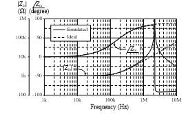 Figure 6: Ideal and simulated frequency responses of the floating lossy series inductor simulator in Figure 2(c).
To show the electronic tunability of the inductor in Figure 2(c), the detailed analysis of frequency characteristic is provided in Figure 7. In the figure, the magnitude responses of the input impedance Zin3 are compared with the ideal series RL impedance by changing the bias current for IB = 50 mA, 200 mA and 400 mA (gm = 0.5 mA/V, 2 mA/V and 4 mA/V).
On the other hand, the simulated transient responses of the proposed floating lossy parallel inductor of Figure 2(d) are given in Figure 8. In this case, the active and passive components are taken as follows: IB = 100 mA (gm = 1 mA/V), R4 = 1 kW and C4 = 1 nF, which yields Req4 = 1 kW and Leq4 = 1 mH. In Figure 8, a sinusoidal input signal was applied to the input of the inductor at a frequency of 200 kHz and signal amplitude of 50 mV peak. The phase difference between vin and i1 is approximately 36°, which is close to the ideal value (tan-1(Req4/wLeq4) = tan-1(1´103)/(2p´200´103´1´10-3) = 38.51°) with a percentage deviation of 6.52%. The tuning capability of the proposed floating lossy parallel inductor has also been tested for IB1 = 50 mA, 200 mA, and 400 mA, while keeping IB2 constant at 100 mA. The resulting frequency characteristics showing in Figure 10 prove that the proposed inductor circuit can be conveniently tuned by electronic means.
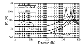 Figure 7: Simulated frequency responses for Zin3 in Figure 2(c) with IB tuning
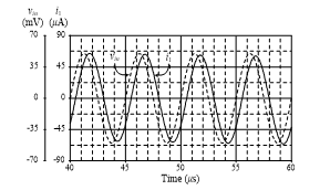 Figure 8: Simulated transient responses of the floating lossy parallel inductor
in Figure 2(d)
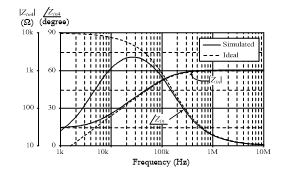 Figure 9: Ideal and simulated frequency responses of the floating lossy parallel inductor simulator in Figure 2(d)
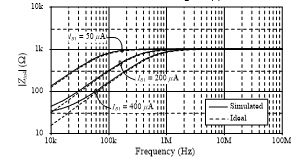 Figure 10: Simulated frequency responses for Zin4 in Figure 2(d) with IB1 tuning.
6. Experimental Results
To further represent the validity of the presented theory, the proposed circuits of Figure 2 were implemented in prototype hardware using IC LT1228 from Linear Technology. The LT1228 is biased with ±5 V supplies. For the experimental testing of Figure 2(a) and 2(b), the passive components in the schematic diagram are the following values: R1 = R2 = 1 kΩ and C1 = C2 = 1 nF. The measured magnitude and phase responses of the proposed grounded series lossy inductor in Figure 2(a) for IB = 50 mA, 100 mA, 200 mA, and 400 mA are shown in Figures 11 and 12, respectively. The calculated and measurement results for the Zin1 frequency responses at a frequency of 100 kHz are summarized in Table 4. According to this table, parasitic gains and signal transfer errors at the corresponding terminals of the LT1228 in conjunction with the tolerances in passive elements used will deviate the impedance frequency responses of the simulated lossy inductor. It should be taken into account the fact that the current and voltage conveying realized by an LT1228 is actually valid under a small-signal operation. However, appropriate adjusting gm with IB gives a significant improvement in the magnitude and phase responses.
In the same manner, the measured frequency responses for the input impedance Zin2 of the proposed grounded parallel lossy inductor in Figure 2(b) are presented in Figures 13 and 14. Regarding the experimental testing for the actively simulated lossy inductor, the results of the Zin2-frequency response at f = 100 kHz is provided in Table 5. Obviously, the practical results are consistent with the theoretical ones. However, the deviation in the magnitude and phase responses is mainly due to the non-ideal parasitic effects and the resistor and capacitor tolerances.
Table 4: Summary of the measured values for the Zin1 in Figure 2(a)
| IB
(mA) |
gm
(mA/V) |
| Zin1 | (kΩ) | ∠Zin1 (degree) | ||
| Measured | Calculated | Measured | Calculated | ||
| 50 | 0.5 | 2.98 | 2.36 | 26.51 | 32.14 |
| 100 | 1 | 1.39 | 1.18 | 32.40 | 32.14 |
| 200 | 2 | 0.84 | 0.59 | 44.11 | 32.14 |
| 400 | 4 | 0.38 | 0.29 | 50.11 | 32.14 |
Table 5: Summary of the measured values for the Zin2 in Figure 2(b)
| IB
(mA) |
gm
(mA/V) |
| Zin2 | (Ω) | ∠Zin2 (degree) | ||
| Measured | Calculated | Measured | Calculated | ||
| 50 | 0.5 | 536.14 | 782.48 | 53.94 | 38.51 |
| 100 | 1 | 440.83 | 532.02 | 63.54 | 57.86 |
| 200 | 2 | 232.05 | 299.72 | 81.17 | 72.56 |
| 400 | 4 | 126.62 | 155.12 | 80.73 | 81.07 |
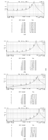 Figure 11: Measured magnitude responses of the proposed grounded series lossy inductor in Figure 2(a)
(a) IB = 50 mA (b) IB = 100 mA (c) IB = 200 mA (d) IB = 400 mA
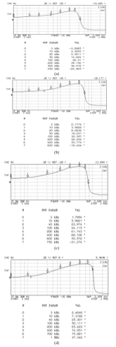 Figure 12: Measured phase responses of
the proposed grounded series lossy inductor in Figure 2(a)
(a) IB = 50 mA (b) IB = 100 mA (c) IB = 200 mA (d) IB = 400 mA
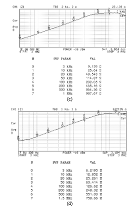 Figure 13: Measured magnitude responses of the proposed grounded series lossy inductor in Figure 2(b)
(a) IB = 50 mA (b) IB = 100 mA (c) IB = 200 mA (d) IB = 400 mA
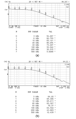
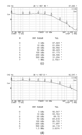 Figure 14: Measured phase responses of
the proposed grounded series lossy inductor in Figure 2(b)
(a) IB = 50 mA (b) IB = 100 mA (c) IB = 200 mA (d) IB = 400 mA
7. Example of Application
To illustrative an application example, the proposed inductor topologies in Figures 2(b) and 2(c) are used for the simulation of serial RL and parallel RL elements of the bandpass filter in Figure 15. The voltage transfer function of Figure 15 is found as:
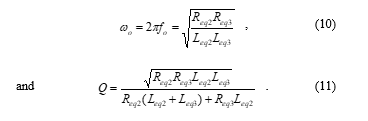
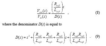 From Equations (8)-(9), the natural angular frequency (ωo) and the quality factor (Q) of the proposed filter in Figure 15 can be characterized as given respectively by the following equations:
 In the simulation, the element values for bandpass filter in Figure 15 with fo = 159.15 kHz and Q = 0.33 are specified as follows: gm = 1 mA/V (IB = 100 μA), R2 = R3 = 1 kΩ, C2 = C3 = 1 nF. Figure 16 shows the plots of the theoretical and simulated frequency responses of the filter, in which Req2 = Req3 = 1 kΩ and Leq2 = Leq3 = 1 mH. From Figure 16, the simulated fo is 156.15 kHz, where the relative error is found as 1.88%.
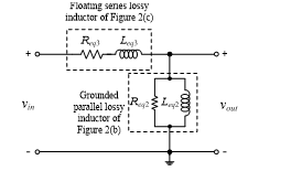 Figure 15: Voltage-mode bandpass filter realization using the proposed actively simulated inductors of Figure 2(b) and 2(c).
8. Conclusions
In this study, the actively simulated grounded/floating lossy inductance simulators using commercially available IC named LT1228 are reported. All of the reported topologies employ a capacitor and a resistor as passive elements and can be tuned electronically through the bias current of the LT1228. The simulation and experimental testing results are achieved to validate their practical performances.
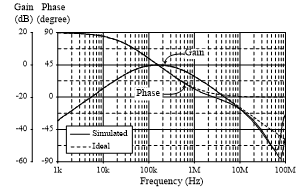 Figure 16: Ideal and simulated frequency responses of the filter in Figure 15
Conflict of Interest
The authors declare no conflict of interest.
Acknowledgment
This work is supported by Faculty of Engineering, King Mongkut’s Institute of Technology Ladkrabang under the contract number 2563-02-01-033.
- A. N. Paul, D. Patranabis, “Active simulation of grounded inductors using a single current conveyor” IEEE Trans. Circuits Syst., 28(2), 164–165, 1981. https://doi.org/10.1109/TCS.1981.1084947
- M. O. Cicekoglu, “Active simulation of grounded inductors with CCII+s and grounded passive elements” Int. J. Electron., 85(4), 455–462, 1998. https://doi.org/10.1080/002072198134003
- M. Srivastava, K. Bhardwaj, A. Roy, A. Singh, “An active-C realization for simulating electronically controllable lossy grounded inductance” in 6th International Conference on Signal Processing and Integrated Networks (SPIN), Noida, India, 137–140, 2019. https://doi.org/10.1109/SPIN.2019.8711758
- O. Cicekoglu, A. Toker, H. Kuntman, “Universal immittance function simulators using current conveyors” Computers and Electrical Eng., 27, 227–238, 2001. https://doi.org/10.1016/S0045-7906(00)00018-5
- M. Faseehuddin, J. Sampe, S. Shireen, S. H. M. Ali, “Lossy and lossless inductance simulators and universal filters employing a new versatile active block” Informacije MIDEM, 48(2), 97–113, 2018.
- M. Dogan, E. Yuce, “CFOA based a new grounded inductor simulator and its applications” Microelectron. J., 90, 297–300, 2019. https://doi.org/10.1016/j.mejo.2019.07.002
- H. Kuntman, M. Gulsoy, O. Cicekoglu, “Actively simulated grounded lossy inductors using third-generation current conveyors” Microelectron. J., 31, 245–250, 2000. https://doi.org/10.1016/S0026-2692(99)00108-1
- H. Y. Wang, C. T. Lee, “Systematic synthesis of R-L and C-D immittances using single CCIII” Int. J. Electron., 87(3), 292–301, 2000. https://doi.org/10.1080/002072100132192
- F. Kacar, A. Yesil, “Novel grounded parallel inductance simulators realization using a minimum number of active and passive components” Microelectron. J., 41, 632–638, 2010. https://doi.org/10.1016/j.mejo.2010.06.011
- B. Metin, “Supplementary inductance simulator topologies employing single DXCCII” Radioengineering, 20(3), 614–618, 2011.
- M. Incekaraoglu, U. Cam, “Realization of series and parallel R-L and C-D impedances using single differential voltage current conveyor” Analog Integr. Circ. Signal Process., 43, 101–104, 2005. https://doi.org/10.1007/s10470-005-6577-8
- U. Cam, F. Kacar, O. Cicekoglu, H. Kuntman, A. Kuntman, “Novel grounded parallel immittance simulator topologies employing single OTRA” Int. J. Electron. Commun. (AEU), 57(4), 287–290, 2003. https://doi.org/10.1078/1434-8411-54100173
- E. Yuce, “Novel lossless and lossy grounded inductor simulators consisting of a canonical number of components” Analog Integr. Circ. Signal Process., 59, 77–82, 2009. https://doi.org/10.1007/s10470-008-9235-0
- F. Kacar, H. Kuntman, “CFOA-based lossless and lossy inductance simulators” Radioengineering, 20(3), 627–631, 2011.
- H. Alpaslan, E. Yuce, “Inverting CFOA based lossless and lossy grounded inductor simulators” Circuits Syst. Signal Process., 34, 3081–3100, 2015. https://doi.org/10.1007/s00034-015-0004-x
- J. K. Pathak, A. K. Singh, R. Senani, “New canonic lossy inductor using a single CDBA and its application” Int. J. Electron., 103(1), 1–13, 2016. https://doi.org/10.1080/00207217.2015.1020884
- A. Yesil, F. Kacar, “New DXCCII-based grounded series inductance simulator topologies” Istanbul University-Journal of Electrical and Electronics Engineering (IU-JEEE), 14(2), 1785–1789, 2014.
- E. Basak, F. Kacar, “Lossy/lossless grounded inductance simulators using current feedback operational amplifier (CFOA)” Electrica, 18(1), 95–99, 2018. https://doi.org/10.5152/iujeee.2018.1815
- R. Singh, D. Prasad, “Grounded lossy inductance simulator using single FTFNTA” in IEEE 17th India Council International Conference (INDICON), New Delhi, India, pp. 1–6, 2020. https://doi.org/10.1109/INDICON49873.2020.9342507
- H. Alpaslan, E. Yuce, “Current-mode biquadratic universal filter design with two terminal unity gain cells” Radioengineering, 21(1), 304–311, 2012.
- U. Cam, F. Kacar, O. Cicekoglu, H. Kuntman, A. Kuntman, “Novel two OTRA-based grounded immitance simulator topologies” Analog Integr. Circ. Signal Process., 39, 169–175, 2004. https://doi.org/10.1023/B:ALOG.0000024064.73784.58
- F. Kacar, A. Yesil, S. Minaei, H. Kuntman, “Positive/negative lossy/lossless grounded inductance simulators employing single VDCC and only two passive elements”, Int. J. Electron. Commun. (AEU), 68(1), 73–78, 2014. https://doi.org/10.1016/j.aeue.2013.08.020
- S. Minaei and E. Yuce, “Realization of tunable active floating inductance simulators” Int. J. Electron., 95(1), 27–37, 2008. https://doi.org/10.1080/00207210701809333
- R. Senani, “New single-capacitor simulation of floating inductors” Electrocomponent Science and Technology, 10, 7–12, 1982. https://doi.org/10.1155/APEC.10.7
- R. Senani and D. R. Bhaskar, “New lossy/loss-less synthetic floating inductance configuration realized with only two CFOAs” Analog Integr. Circ. Sig. Process., 73, 981–987, 2012. https://doi.org/10.1007/s10470-012-9897-5
- R. Senani, “New tunable synthetic floating inductors” Electron. Lett., 16(10), 382–383, 1980. https://doi.org/10.1049/el:19800270
- D. R. Bhaskar and R. Senani, “Synthetic floating inductors realized with only two current feedback op-amps” American J. Electrical Electron. Eng., 3(4), 88–92, 2015.
- E. Yuce, “New low component count floating inductor simulators consisting of a single DDCC” Analog Integr. Circ. Sig. Process., 58, 61–66, 2009. https://doi.org/10.1007/s10470-008-9218-1
- M. A. Ibrahim, S. Minaei, E. Yuce, N. Herencsar and J. Koton, “Lossy/lossless floating/grounded inductance simulation using one DDCC” Radioengineering, 21(1), 3–10, 2012.
- E. Yuce, S. Tokat, H. Alpaslan, “Grounded capacitor-based new floating inductor simulators and a stability test” Turk. J. Elec. Eng. & Comp. Sci., 23, 2138–2149, 2015. http://doi.org/10.3906/elk-1301-183
- M. T. Abuelma’atti, S. K. Dhar, Z. J. Khalifa, “New two-CFOA-based floating immittance simulators” Analog Integr. Circ. Sig. Process., 91, 479–489, 2017. https://doi.org/10.1007/s10470-017-0956-9
- R. Sotner, N. Herencsar, J. Jerabek, A. Kartci, J. Koton, T. Dostal, “Pseudo-differential filter design using novel adjustable floating inductance simulator with electronically controllable current conveyors” Elektron. Elektrotech., 23(2), 31–35, 2017. https://doi.org/10.5755/j01.eie.23.2.17996
- A. Abaci, E. Yuce, “Single DDCC based new immittance function simulators employing only grounded passive elements and their applications” Microelectron. J., 83, 94–103, 2019. https://doi.org/10.1016/j.mejo.2018.11.014
- A. Abaci, E. Yuce, “Single DDCC-based simulated floating inductors and their applications” IET Circuits, Devices & Systems, 14(6), 796–804, 2020. https://doi.org/10.1049/iet-cds.2019.0558
- N. Roongmuanpha, W. Tangsrirat, “SITO current-mode multifunction biquad using readily available IC LT1228s”, in The 6th International Conference on Engineering, Applied Sciences and Technology (ICEAST-2020), July 1-4, Thailand, pp. 108-111, 2020. https://doi.org/10.1109/iceast50382.2020.9165538
- R. Sotner, N. Herencsar, J. Jerabek, L. Langhammer, J. Polak, “On practical construction of electronically controllable compact current amplifier based on commercially available elements and its application”, Int. J. Electron. Commun. (AEU), 81(11), 56-66, 2017. https://doi.org/10.1016/j.aeue.2017.07.002
- N. Roongmuanpha, T. Pukkalanun, W. Tangsrirat, “Practical realization of electronically adjustable universal filter using commercially available IC-based VDBA” Engineering Review, 41(3), 2020. https://doi.org/10.30765/er.1547
- P. Moonmuang, N. Roongmuanpha, T. Pukkalanun, W. Tangsrirat, “On the realization of simulated lossy inductors using voltage differencing buffered amplifiers” in 2020 8th International Electrical Engineering Congress (iEECON), Chiang Mai, Thailand, 2020. https://doi.org/ 10.1109/iEECON48109.2020.229469
- Linear Technology, “100MHz current feedback amplifier with DC gain control”, LT1228 datasheet, 1994.