
A Rectification Circuit with Co-Planar Waveguide Antenna for 2.45 GHz Energy Harvesting System
Volume 6, Issue 2, Page No 984-989, 2021
Author’s Name: Nuraiza Ismaila), Ermeey Abd Kadir
View Affiliations
Faculty of Electrical Engineering, Universiti Teknologi MARA, Shah Alam, Selangor, 40450, Malaysia
a)Author to whom correspondence should be addressed. E-mail: nuraizaismail@gmail.com
Adv. Sci. Technol. Eng. Syst. J. 6(2), 984-989 (2021); ![]() DOI: 10.25046/aj0602113
DOI: 10.25046/aj0602113
Keywords: Co-Planar Waveguide, RF Energy Harvesting, AC-DC Conversion

Export Citations
A new approach for designing RF energy harvester with a single stage converter circuit is presented in this paper. The proposed converter configuration is integrated with an antenna that is based on the coplanar waveguide (CPW) transmission line with improved gain resonated at 2.45 frequency ISM band. The CPW patch antenna as a harvester antenna is designed in a rectangular shape that uses FR-4 substrate with a loss tangent and relative permittivity of 0.025 and 4.3 respectively. The output from the harvester antenna is connected to the converter circuit using only two Schottky diodes. The rectifier design achieves between 0.1% to 37% of RF-DC power conversion efficiency over the ambient RF input signal range from -20 dBm to 0 dBm and the antenna exhibits a directivity of 3.896 dBi as well as a return loss of -48.85 dB. For an input power of 0 dBm, the proposed circuit can rectify an AC signal up to 6.09 V. Moreover, the proposed CPW antenna that is integrated with a converter circuit agrees for the harvesting of ambient electromagnetic energy to power low power electronic devices.
Received: 24 January 2021, Accepted: 07 April 2021, Published Online: 22 April 2021
1. Introduction
Advancements in energy harvesting from the environment or ambient have grown a lot of attention in recent years as ambient energy harvesting delivers a green self-sustainable operation for powering low power electronics devices [1–3]. This technology exploits energy from several sources from the environment, for example solar light, heat, vibration, thermal energy and electromagnetic waves [4, 5]. It has become an alternative for powering low power electronic devices instead of using a conventional method which is battery plug in mainly used in wireless sensor networks of the Internet of Things (IoT), wearable electronic devices and implantable biomedical devices[6–9].
Today, batteries remain the vital source to power up these system devices. Nevertheless, the method has various inherent disadvantages. For instance, the battery size and weight are huge, limitation of battery lifespan and also requires more cost of battery replacement for these devices [8, 10–12]. To over come these drawbacks, engineers have exploited a new approach called energy harvesting , to extend the battery life and empower an autonomous manoeuvre of the IoT end nodes [13, 14]. The energy harvesting has rendered an attractive approach for energizing low power electronic devices [2, 15]. It empowers wireless charging, battery-less and a reasonable alternative for supplying the wireless nodes even in cold, dark, and static environments without requiring power cables or battery replacement [14, 16–18].
The past decade has seen an increase in the use of an ambient environment as the source of radio frequency (RF) energy harvesting. This harvesting system is the most prominent of its accessibility and easy scavenging system compared to other sources. Other sources are far from human control as thermal energy requires heat, vibration needs motion while solar requires light present [19, 20]. This alternative approach used the concept of capturing the ambient power, including the wasted power that hovering in the surrounding environment without any distraction to the environment [21–23]. In contrast, the naturally low ambient RF energy can be significantly challenging. Also, it is easily carried or wear, especially when the RF energy harvester is combined with completely autonomous systems due to its low input power and voltage necessities [24, 25]. To overcome this issue, the Schottky diode has been commonly used for RF energy harvesting as it has a minimum threshold voltage and fast switching diode speed [10, 13].
The RF energy harvesting system comprises an antenna that captures an RF incoming signal, a network that represents impedance matching for exploiting power transfer from the antenna and the rectifier or converter circuit. The rectifier circuit is a key component in the system block which determines the system efficiency. It converts the RF signal to DC voltage and stores the energy in holding load storage devices such as capacitor and battery. Figure 1 illustrates the basic block diagram of energy harvesting structures. The following sections describe four main parts of this system.
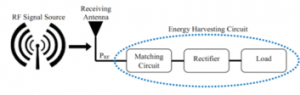
Figure 1: Block diagram of RF energy harvesting system [13]
The major challenge in designing an ambient RF energy harvesting system is the requirement to operate with low power RF signals. The works published in [13,26,27] have achieved the maximum power conversion efficiency (PCE) of the rectifier at relatively high input power levels, which is above 5 dBm while the available ambient RF signals are much lower levels in the environment which are lower than -15 dBm. In order to reach high maximum PCE, multistage rectifier is the most commonly used technique among previous reseachers [28,29]. Nevertheless, the high power efficiency results from high input RF signals that are applied to the multistage rectifier. The circuit designed in [30] needs four stages in rectifier configuration for their circuit optimization when -15 dBm input power signal is applied. They observed that the number of stages does not help to improve efficiency for low power RF input signal. As the number of stages increases, the peak of the efficiency curve decreases toward higher powers.
This paper is an expansion of work originally reported in Proceedings of the 2019 IEEE Asia-Pacific Conference on Applied Electromagnetics (APACE) [31]. In the previous work, a square patch antenna was designed and analysed with a matching converter circuit. In this proposed work, the antenna and the rectifier of the converter circuit have been enhanced for both parts. This work also highlights a single RF energy harvesting circuit that aims to convert the power within the 2.45 frequency band RF signal into usable DC supply. As compared with previous work [31], the gain of the enhancement antenna has been improved. Meanwhile, the ripple voltage of the output signal that occurred in previous work has been resolved with a new arrangement of components in converter circuit design. In the end, a novel RF energy harvesting system using only one stage converter circuit is presented which is able to harvest low input power signal.
2. Harvesting Antenna Design
An antenna is required in the receiving part for harvesting RF energy as it captures energy from ambient. The RF energy is then rectified and converted into DC voltage. The proposed harvesting antenna design as illustrated in Figure 2 is a rectangular patch antenna with co-planar waveguide feed. This arrangement is preferred due to its simple impedance matching and high circuit density on one layer. Besides, its active and passive elements are easy to integrate and it has low dispersion and low radiation loss. All these make the co-planar waveguide preferable for rectifying circuit design.
The low-cost FR-4 substrate with a dielectric constant 4.3, tan δ = 0.025 and thickness of 1.6 mm are used for designing the proposed CPW antenna. The area of 30 × 38 mm2 where the width and length area calculated using equation (1) and (2) respectively. This antenna is excited by a feeding line of 50 Ω characteristic impedance with a width of 4.235 mm. Both gaps between the feeding line and the ground plane are g = 0.5 mm. The detailed geometry structure of the proposed antenna design after optimization is shown in Table 1.
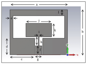
Figure 2: Geometry of the proposed antenna based on co-planar waveguide feed
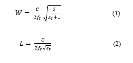
Table 1: The Proposed Antenna Parameters
| Parameter | (mm) |
| a | 38.0 |
| b | 30.0 |
| c | 16.4 |
| d | 11.0 |
| e | 2.0 |
| f | 6.0 |
| g | 4.4 |
| h | 6.0 |
| i | 0.5 |
| j | 17.0 |
| k | 9.0 |
| l | 4.0 |
3. Converter Circuit Design
In the RF energy harvesting system, a rectifier circuit is required for converting RF input energy into funtional DC energy. The rectifier that acts as a converter circuit converts the AC input signal from the RF source. AC to DC conversion is required for this system as the RF source is being received in the form of a sine wave signal. Hence, the RF source is represented by a sinusoidal voltage source Vs as depicted in Figure 3. The arrangement of rectifier circuit contains three parts which are a matching network, a conversion circuit and a load. The converter circuit and the circuit components with parameters after optimization are shown in Figure 3 and Table 2 respectively. Two Schottky diodes of MBR0520L are used for the rectification process. The Schottky diode is preferred due to its attractive feature of low substrate losses and quick switching. Moreover, the Schottky diode has a high sensitivity to the very small ambient signal.
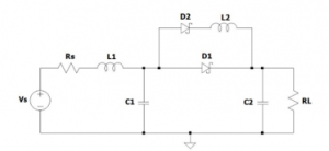
Figure 3: The proposed RF harvesting converter circuit using Schottky connected diodes
For simulation study, Vs is connected to the converter circuit in a sinusoidal source that represents an RF energy harvester from the receiving antenna. The antenna port impedance represented by internal resistance, Rs is set to 50 Ω. In this circuit topology, the matching circuit is simply constructed using capacitor C1 and inductor L1. This matching circuit is required to match their impedances between the receiving antenna and converter circuit where a good matching network will allow a maximum power transfer between them. The vital part in this harvesting circuit is the conversion where it rectifies RF input signal to DC signal. Both Schottky diodes and inductor L2 are needed for this circuit to convert AC to DC signal. In this circuit design, the capacitor C2 is important in order to eliminate ripple DC voltage that occurs at the output terminal. After the DC signal is passed through the DC bypass filter, then it appears as a useable voltage across the load, RL.
Table 2: Circuit Components and Parameters
| Components | Value | Unit |
| Rs | 50 | Ω |
| L1 | 33 | nH |
| L2 | 3 | nH |
| C1 | 1 | pF |
| C2 | 33 | uF |
| RL | 100 | kΩ |
The circuit analysis examines the constant input ac voltage with low amplitude sinusoidal voltage and it is separated into four operating modes for each cycle.
Mode 1: During the positive half input cycle, the inductor, L and capacitor, C1 are charged by the sinusoidal voltage source. Both D1 and D2 are in OFF state. The load, RL is feed by the energy stored in the C2 that acts as a filter capacitor.
Mode 2: The mode starts when VC1 = VIN – VL > VOUT, where Diode D2 is switched to ON state. The capacitor C2 is energized. All the energy stored in L1 and C1 during Mode 1 is fed to the load. The saturated current of inductor, L1 and capacitor, C1 drops linearly. The changing state of D2 influence the loss during this mode.
Mode 3: This mode happens as VIN = VC1 + VL2 > VOUT, D2 is switched to ON state. As capacitor C2 is energizing, the energy stored in L2 and C1 during Mode 3 is transferred to the load. The changing state of D1 influences the loss during this mode.
Mode 4: When VC1 and VL1 + VC1 > VOUT, the diodes, D1 and D2 are switched to ON state. The load is driven by the energy stored in L1 and C1 as they transferred to the load through L2 and C2.
4. Results and Discussion
The simulation results are discussed in two parts; the receiving antenna and the converter circuit design.
4.1. Receiving Antenna
The receiving antenna design has been simulated using CST Microwave Studio Software. Before connecting to the converter circuit, the proposed CPW antenna is analysed separately by evaluating the S-parameters. This is to ensure the performance of the proposed antenna achieve a good return loss with perfect matching impedance ( 50 Ω) and better gain compared to previous work. Figure 4 indicates the simulation result for return loss, S11 is -48.85 dB at 2.4976 GHz resonating frequency. The operating bandwidth of 309 MHz in the range between 2.3618 to 2.707 GHz, covers the IEEE 802.11 standard in the 2.45 GHz wireless ISM band. Matching impedance is approximate to 50 Ω while VSWR is 1.007 as shown in Figure 5 and Figure 6 respectively. Since the value of VSWR is under 2, the proposed antenna is worth mentioning that it has a good match and is applicable for most antenna applications.
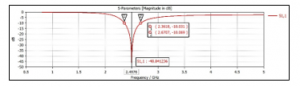
Figure 4: Return loss simulation result of proposed CPW antenna
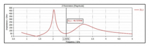
Figure 5: Line impedance at 2.4976 resonant frequency
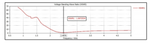
Figure 6: Voltage standing wave ratio (VSWR) for the CPW antenna
The good values of S11 and VSWR are insufficient to prove an antenna has good radiation. Antenna gain is one of the key elements that needs to be considered in antenna design as it is an essential metric. The gain of an antenna highlights how much transmitted power in the direction of peak directivity to that of radiation energy. The simulated far-field radiation pattern can be observed in Figure 7 where it shows the gain and the 3-D forward directional pattern of the proposed CPW antenna. The gain of this antenna is 3.896 dBi and it is better compared to previous work [31] which is less than 1 dBi.
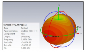
Figure 7: Simulated 3-D radiation pattern of CPW antenna
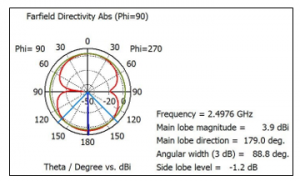
Figure 8: Simulated 2-D radiation pattern
Figure 8 indicates the main and side lobes of the proposed antenna. From this simulated 2-D radiation pattern figure, it indicates that the dipole antenna has an elevation plane beamwidth of 88.8 degrees. Since all metal patches of the substrate for this proposed CPW antenna are designed on one side, the antenna radiates in both front and back directions.
4.2. Converter Circuit
To determine the harvested voltage and current, LTSpice software is used to simulate the converter circuit. The output voltage and current for 0 dBm input power are depicted in Figure 9. From this output, it shows that both output current and voltage are simultaneously harvested to 6.09 V and 0.06 mA respectively. In this work, the ripple output voltage is successfully eliminated as compared to previous work that had large ripple voltage [31].
Equation (3) is the RF to DC power conversion efficiency (PCE) which is defined as the ratio of the DC power PDC and the RF power PRF, where PDC is the dc power produced at the load resistance while PRF is the power received by the antenna.
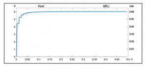
Figure 9: The output voltage and current obtained from the converter circuit for 0 dBm RF input power
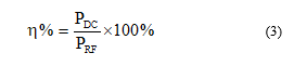
Table 3 shows the output voltage and the PCE for every single input power level. Both the output voltage and efficiency of the circuit are increased as the input power varies from -20 dBm to 0 dBm. As seen in Figure 10, the DC output voltage exceeds 6.09 V with 37.0% efficiency when the input power is 0 dBm. Hence, the energy stored in capacitor C2 is 100.5 µJ.
Table 3: The output voltage and PCE with respect to five different input power levels
| Input Power
(dBm) |
Output Voltage
(V) |
PCE
(%) |
| -20 | 0.02 | 0.1 |
| -15 | 0.12 | 0.5 |
| -10 | 0.52 | 2.7 |
| -5 | 1.85 | 10.9 |
| 0 | 6.09 | 37.0 |
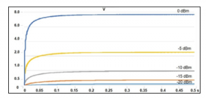
Figure 10: The output voltages with respect to different input power level
4.3. S-Parameter Analysis
The antenna and the converter circuit are matched to maximize the stored energy. Results from S-parameter are used to analyze the signal performance of the converter circuit regarding the difference in circuit component value. Figure 11 shows the connection between the CPW antenna and the converter circuit by using CST Microwave Studio integrated with CST Design Studio.
Table 4: Performance summary and distinction with related works
|
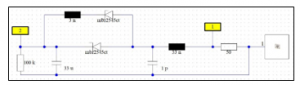
Figure 11: The integrated of the proposed CPW antenna and converter circuit
The result of the S-parameter for the proposed antenna integrated with the converter circuit is simulated by using CST Design Studio as illustrated in Figure 12. The results for both return loss, |S11| = 0.197 and transfer coefficient |S21| = 0.4 at 2.4659 GHz frequency are good since the magnitude value of |S11| and |S21| are ideal to be close to 0.1 and 1 respectively.
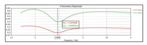
Figure 12: The circuit return loss |S11| and transfer coefficient |S21|
4.4. Comparison with Previous Work
Table 4 summarizes a distinction between the proposed study and previous researchers’ work based on rectifier used. Since the incident power can never be 0 dBm for 900 MHz and 2.45 GHz ISM band, the comparison is made up of input power between -15 dBm to -20 dBm. As observed at the input power level of -15 dBm, this work provides a low cost antenna substract with lower PCE compared to [32]. However, the load resistance in [32] is 10 times greater than this work, which contributes large power efficiency. In terms of the PCE, this proposed work indicates the lowest performance as compared to the same type of rectifier used in [7] and [33]. Nevertheless, the output voltage in this work is not much different compared to both of them. Meanwhile, reference [24] shows the second highest power conversion effiency among other work, but the load resistance used is also high, which is 5 times greater than this work. Besides, the proposed circuits in [16] and [24] are much more costly since they use 10 cascoded and 10 stages of CMOS respectively. The power efficiency in this proposed work needs to be optimized to give higher efficiency. This can be done by optimizing the impedance matching between the antenna and the rectifier circuit. Moreover, diode characteristics need to be considered since this work uses only non-zero bias diode which degrades the power efficiency. Besides, the influence of saturation current of schottky diode to output voltage needs to be investigated.
5. Conclusion
In this work, a coplanar waveguide antenna with a gain of 3.896 dBi at the resonated frequency of 2.4976 GHz is analyzed for RF energy harvesting applications. A setup has been employed here to study the behaviour of the co-planar waveguide antenna integrated with two Schottky diodes in converter circuit design. Our proposed design has returned very satisfactory results that are applicable for the 2.45 GHz ISM band. The proposed converter circuit specifies the input power can be rectified up to 6.09 V DC signal with power conversion efficiency of 37% and energy of 100.5 µJ for input power of 0 dBm. The findings indicated that a sinusoidal RF incoming signal can be converted to a smooth DC voltage using a proposed RF energy harvesting circuit for powering wireless sensor nodes. For future improvements, matching impedance, diode characteristics and saturation current are essential for improving power efficiency.
- B.S. Kim, R. Vyas, J. Bito, K. Niotaki, A. Collado, A. Georgiadis, M.M. Tentzeris, “Ambient RF Energy-Harvesting Technologies for Self-Sustainable Standalone Wireless Sensor Platforms,” Proceedings of the IEEE, 102(11), 2014, doi:10.1109/JPROC.2014.2357031.
- T.A. Elwi, H.S. Ahmed, “A UWB Monopole Antenna Design based RF Energy Harvesting Technology,” 2018 Third Scientific Conference of Electrical Engineering (SCEE), 111–115, 2018, doi:10.1109/SCEE.2018.8684112.
- R. Ren, J. Huang, H. Sun, “Investigation of Rectenna’s Bandwidth for RF Energy Harvesting,” 2020 IEEE MTT-S International Microwave Workshop Series on Advanced Materials and Processes for RF and THz Applications, IMWS-AMP 2020 – Proceedings, 2020, doi:10.1109/IMWS-AMP49156.2020.9199653.
- S. Adami, V. Marian, N. Degrenne, C. Vollaire, B. Allard, F. Costa, “Self-Powered Ultra-low Power DC-DC Converter for RF Energy Harvesting,” 2012 IEEE Faible Tension Faible Consommation, 1–4, 2012, doi:10.1109/FTFC.2012.6231746.
- H. Ulusan, K. Gharehbaghi, O. Zorlu, A. Muhtaroglu, H. Kulah, “An efficient integrated interface electronics for electromagnetic energy harvesting from low voltage sources,” 2013 Transducers and Eurosensors XXVII: The 17th International Conference on Solid-State Sensors, Actuators and Microsystems, TRANSDUCERS and EUROSENSORS 2013, (June), 450–453, 2013, doi:10.1109/Transducers.2013.6626800.
- S.M. Noghabaei, R.L. Radin, M. Sawan, “Efficient dual-band ultra-low-power RF energy harvesting front-end for wearable devices,” Midwest Symposium on Circuits and Systems, 2018-Augus, 444–447, 2019, doi:10.1109/MWSCAS.2018.8623832.
- V. Palazzi, J. Hester, J. Bito, F. Alimenti, C. Kalialakis, A. Collado, P. Mezzanotte, A. Georgiadis, L. Roselli, M.M. Tentzeris, “A Novel Ultra-Lightweight Multiband Rectenna on Paper for RF Energy Harvesting in the Next Generation LTE Bands,” IEEE Transactions on Microwave Theory and Techniques, 66(1), 366–379, 2018, doi:10.1109/TMTT.2017.2721399.
- U. Muncuk, K. Alemdar, J.D. Sarode, K.R. Chowdhury, “Multiband ambient RF energy harvesting circuit design for enabling batteryless sensors and IoT,” IEEE Internet of Things Journal, 5(4), 2700–2714, 2018, doi:10.1109/JIOT.2018.2813162.
- C.H. Lin, C.W. Chiu, J.Y. Gong, “A Wearable Rectenna to Harvest Low-Power RF Energy for Wireless Healthcare Applications,” Proceedings – 2018 11th International Congress on Image and Signal Processing, BioMedical Engineering and Informatics, CISP-BMEI 2018, 1–5, 2019, doi:10.1109/CISP-BMEI.2018.8633222.
- J. Bito, R. Bahr, J.G. Hester, S.A. Nauroze, A. Georgiadis, M.M. Tentzeris, “A Novel Solar and Electromagnetic Energy Harvesting System with a 3-D Printed Package for Energy Efficient Internet-of-Things Wireless Sensors,” IEEE Transactions on Microwave Theory and Techniques, 65(5), 1831–1842, 2017, doi:10.1109/TMTT.2017.2660487.
- L. Xia, J. Cheng, N.E. Glover, P. Chiang, “0.56 V, -20 dBm RF-powered, multi-node wireless body area network system-on-a-chip with harvesting-efficiency tracking loop,” IEEE Journal of Solid-State Circuits, 49(6), 1345–1355, 2014, doi:10.1109/JSSC.2014.2305074.
- F. Yuan, Q.T. Zhang, S. Jin, H. Zhu, “Optimal harvest-use-store strategy for energy harvesting wireless systems,” IEEE Transactions on Wireless Communications, 14(2), 698–710, 2015, doi:10.1109/TWC.2014.2358215.
- M.M. Mansour, H. Kanaya, “High-Efficient Broadband CPW RF Rectifier for Wireless Energy Harvesting,” IEEE Microwave and Wireless Components Letters, 29(4), 288–290, 2019, doi:10.1109/LMWC.2019.2902461.
- A. Ercan, M.O. Sunay, I.F. Akyildiz, “RF Energy Harvesting and Transfer for Spectrum Sharing Cellular IoT Communications in 5G Systems,” IEEE Transactions on Mobile Computing, 17(7), 1680–1694, 2018, doi:10.1109/TMC.2017.2740378.
- D. Mishra, S. De, D. Krishnaswamy, “Dilemma at RF Energy Harvesting Relay: Downlink Energy Relaying or Uplink Information Transfer?,” IEEE Transactions on Wireless Communications, 16(8), 4939–4955, 2017, doi:10.1109/TWC.2017.2704084.
- M. Stoopman, K. Philips, W.A. Serdijn, “An RF-Powered DLL-Based 2.4-GHz Transmitter for Autonomous Wireless Sensor Nodes for Autonomous Wireless Sensor Nodes,” IEEE Transactions on Microwave Theory and Techniques, 65(7), 1–10, 2017, doi:10.1109/TMTT.2017.2651817.
- R.K. Sidhu, J. Singh Ubhi, A. Aggarwal, “A Survey Study of Different RF Energy Sources for RF Energy Harvesting,” 2019 International Conference on Automation, Computational and Technology Management, ICACTM 2019, 530–533, 2019, doi:10.1109/ICACTM.2019.8776726.
- W. Ni, S. Member, X. Dong, S. Member, “Energy Harvesting Wireless Communications With Energy Cooperation Between,” IEEE Transactions on Communications, 63(4), 1457–1469, 2015, doi:10.1109/TCOMM.2015.2404777.
- I. Adam, M.N.M. Yasin, M.E.A. Aziz, M.I. Sulaiman, “Rectifier for RF energy harvesting using stub matching,” Indonesian Journal of Electrical Engineering and Computer Science, 13(3), 1007–1013, 2019, doi:10.11591/ijeecs.v13.i3.pp1007-1013.
- S. Keyrouz, H.J. Visser, A.G. Tijhuis, “Rectifier analysis for Radio Frequency energy harvesting and Power Transport,” 428–431, 2012, doi:10.23919/eumc.2012.6459081.
- N.A. Eltresy, D.N. Elsheakh, E.A. Abdallah, H.M. Elhennawy, “Tri-Band Antenna for Energizing IoT Low Power Devices,” 2018 IEEE Global Conference on Internet of Things, GCIoT 2018, 1–5, 2019, doi:10.1109/GCIoT.2018.8620145.
- J.C. Wang, M. Leach, Z. Wang, K.L. Man, E.G. Lim, “Rectanna Design for Energy Harvesting,” 2016 IEEE Asia Pacific Conference on Circuits and Systems (APCCAS), 456–457, 2016, doi:10.1109/APCCAS.2016.7804001.
- J.C.S. Kadupitiya, T.N. Abeythunga, P.D.M.T. Ranathunga, D.S. De Silva, “Optimizing RF energy harvester design for low power applications by integrating multi stage voltage doubler on patch antenna,” 2015 8th International Conference on Ubi-Media Computing, UMEDIA 2015 – Conference Proceeedings, 335–338, 2015, doi:10.1109/UMEDIA.2015.7297481.
- S.M. Noghabaei, R.L. Radin, Y. Savaria, M. Sawan, “A High-Efficiency Ultra-Low-Power CMOS Rectifier for RF Energy Harvesting Applications,” 2018 IEEE International Symposium on Circuits and Systems (ISCAS), 18–21, 2018, doi:10.1109/ISCAS.2018.8351149.
- D. Misra, G. Das, D. Das, “An IoT based Wireless Energy Harvesting using Efficient Voltage Doubler Stages in a RF to DC Converter,” 2018 4th International Conference on Computing Communication and Automation (ICCCA), 1–5, 2019, doi:10.1109/ccaa.2018.8777712.
- S. Kim, H. Abbasizadeh, B.S. Rikan, S.J. Oh, Y. Park, D. Khan, T. Thi, K. Nga, K. Kang, S. Member, Y. Yang, K. Lee, S. Member, “A -20 to 30 dBm Input Power Range Wireless Power System with a MPPT-based Reconfigurable 48 % Efficient RF Energy Harvester and 82 % Efficient A4WP Wireless Power Receiver with Open Loop Delay Compensation,” Transactions on Power Electronics, 8993(c), 1–31, 2018, doi:10.1109/TPEL.2018.2872563.
- W. Liu, K. Huang, S. Member, T. Wang, “A Broadband High-Efficiency RF Rectifier for Ambient RF Energy Harvesting,” IEEE Microwave and Wireless Components Letters, 30(12), 50–53, 2020, doi:10.1109/LMWC.2020.3028607.
- N. Pournoori, M.W.A. Khan, L. Ukkonen, T. Björninen, “RF Energy Harvesting System Integrating a Passive UHF RFID Tag as a Charge Storage Indicator,” 2018 IEEE Antennas and Propagation Society International Symposium and USNC/URSI National Radio Science Meeting, APSURSI 2018 – Proceedings, 685–686, 2018, doi:10.1109/APUSNCURSINRSM.2018.8608530.
- M.M. Mansour, S. Yamamoto, H. Kanaya, S. Member, “Reconfigurable Multistage RF Rectifier Topology for 900 MHz ISM Energy-Harvesting Applications,” IEEE Microwave and Wireless Components Letters, 30(12), 1–4, 2020, doi:10.1109/LMWC.2020.3029252.
- U. Muncuk, K. Alemdar, J.D. Sarode, K.R. Chowdhury, “Multiband ambient RF energy harvesting circuit design for enabling batteryless sensors and IoT,” IEEE Internet of Things Journal, 5(4), 2700–2714, 2018, doi:10.1109/JIOT.2018.2813162.
- N. Ismail, M.T. Ali, E.A. Kadir, M. Firdaus, M. Zin, F.N. Mohd, “A Power Converter Circuit of Co-Planar Waveguide RF Harvester Antenna for Low Power Wireless Applications,” 2019 IEEE Asia-Pacific Conference on Applied Electromagnetics (APACE), (November), 25–27, 2019, doi:10.1109/APACE47377.2019.9020999.
- Z. Hameed, K. Moez, “Design of impedance matching circuits for RF energy harvesting systems,” Microelectronics Journal, 62(April 2016), 49–56, 2017, doi:10.1016/j.mejo.2017.02.004.
- D.K. Ho, V. Ngo, I. Kharrat, T.P. Vuong, Q.C. Nguyen, M.T. Le, “A Novel Dual-Band Rectenna for Ambient RF Energy Harvesting at GSM 900 MHz and 1800 MHz,” 2016 IEEE International Conference on Sustainable Energy Technologies (ICSET), 2(3), 612–616, 2017, doi:10.1109/ICSET.2016.7811800.