Simulation of Pulse Width Modulation DC-DC Converters Through Symbolic Analysis Techniques
 , Francesco Grasso, Antonio Luchetta, Stefano Manetti, Alberto Reatti
Adv. Sci. Technol. Eng. Syst. J. 6(1), 275–282 (2021);
 DOI: 10.25046/aj060132
The problem of Pulse Width Modulated (PWM) DC-DC converter simulation is faced in this paper. It is shown how the analysis of this kind of circuits, nonlinear and switching for their nature, can be easily and quickly executed by using symbolic analysis techniques. The paper also presents the program SapWinPE, which performs an automatic symbolic analysis of the considered circuit, and its outputs are in MATLAB compatible format. SapWinpPE features make it more attractive than general-purpose software tools for both academy and industry circuit designers. Other characteristics and potentialities, shown through application examples in the paper, can be advantageously exploited by all the circuit designers and CAD professionals, also at the research and educational level in the academic field.
1.Introduction
In all modern electronic circuits it is nearly impossible to find devices that are not supplied by switching-mode power converters. Most of them use Pulse Width Modulated (PWM) DC–DC converters as output voltage regulators, and their behavior affects the operation of the overall systems. In some applications, the reliability of the supplied systems is linked to the proper behavior of PWM DC-DC converters in such a way to lead to fatal consequences in case of poor design. As an example, it is enough to think about artificial heart implants to understand how a proper design of power converters is crucial.
In the realization of any device, the first step is the theoretical design, which consists of a “pencil and paper” circuit creation. To verify the correctness of the obtained circuit, repeated circuit simulations are needed, where the term “circuit simulation” means the analysis of a theoretical circuit with software tools. In the case of DC-DC converters, this is not an easy and fast task to perform because of the interaction of many devices, their interconnection, sizing, and biasing. Moreover, switched current and voltage waveforms result in high values of their derivatives which run the numerical simulators close to their convergence limits. For this reason, the subject of DC-DC converter simulation has interested many researchers in the last thirty years, but a definitive solution has not yet been found. Also, the authors have faced this problem and this paper is an extension of a work originally presented at the 2019 IEEE 5th International Forum on Research and Technology for Society and Industry (RTSI) [1], where a program, named SapWinPE, was presented. SapWinPE is based on the application of symbolic analysis techniques and this constitutes an important novelty because symbolic programs dedicated to PWM DC-DC converters do not exist, at least to the authors’ knowledge.
This paper aims to better describe the program in [1] from the theoretical, algorithmic, and applicative points of view, by proposing further examples and comparing the obtained results with those deriving from other programs, like PSPICE based programs, and with experimental results. Finally, a new possible method for simulating switching circuits is proposed together with some results obtained with a new program, still in an embryonic state, implementing this new approach.
The paper is so organized. The implementation methodology and the theoretical basis of SapWinPE are presented in Section 2. Section 3 provides a discussion on the reasons which have led to choose symbolic techniques, a program description is proposed in Section 4. Applicative examples and comparisons with other programs are shown in Section 5. In Section 6 a short description of a further approach to the simulation of switching circuits is presented along with an application examples. Finally, Section 7 contains conclusions and future developments.
2. Theoretical Basis
PWM DC-DC converters are time-variant circuits. This feature is due to the presence in many topologies, such as buck, boost, buck-boost, of a particular cell constituted by a switch and a diode. This switching cell, shown in Figure 1(a), operates as a device alternatively channeling the inductor current through the switch and the diode.
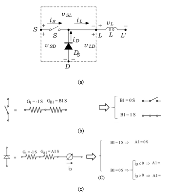 Figure 1: The switching cell in a PWM DC-DC converter. (a) Switching cell. (b) switch model. (c) diode model.
In other converters, such as Cùk, Flyback, and Forward converters, switch and diode are not connected to the same node, but their combination always acts exactly in the same way. A DC-DC converter circuit switches between two different configurations or among three different configurations, depending on the inductor current value: when it has a nonzero value at the end of the switching period T, the circuit works in Continuous Conduction Mode (CCM); when it assumes a zero value before the end of the switching period T, the circuit works in Discontinuous Conduction Mode (DCM). There is also an intermediate operation mode, called Boundary Conduction Mode (BCM), corresponding to the case of zero inductor current exactly at the end of the switching period T: also in this case, the circuit switches between two different configurations. In any case, moving from a configuration to another one causes a topology change, showing in this way the time-variant nature of the circuit [2].
As well known, the Laplace transform can be classically applied to linear time-invariant circuits. Then, even if converters nonlinearities are neglected, its time-variant nature prevents the application of this method. It is nonetheless true that the circuit remains time-invariant within each assumed configuration, then, the Laplace transform can be applied to every switching state. However, proceeding in this way, the inverse Laplace transform must be applied to each configuration and must be evaluated not only the output of interest in the time-domain but also the inductor current and the capacitor voltage in the time‑domain, because their values at the switching instant constitute the initial conditions for the analysis in the subsequent time interval. In short, this approach is not convenient, not only because the time domain responses require several applications of the inverse Laplace transform, but principally because it is not possible to automatically consider the different operating modes. To circumvent this strong limitation, it is necessary to model the switching cell as a single device whose switching behavior is directly controlled by internal parameters. The switching cell model must have an additional feature: it must be able to take automatically into account the state of the switches via parameter settings. In this way, a circuit depending on the characteristic parameters of the switching cell model can be obtained. Under any switching state, the circuit configuration assumed by the power converter is linear and time-invariant for any switching period, and also in its whole working time: thus the model becomes Laplace transformable. Circuit transfer functions in closed form, dependent on the state of the switches and on the initial conditions of capacitors and inductors at each switching time, can be so obtained. The working conditions determine the parameter values. Proceeding in this way, it is still necessary to apply the inverse Laplace transform in each switching interval for evaluating the time domain responses, but the different operation modes are automatically determined.
The switch model [3] is shown in Figure 1(b). A conductance, equal to −1 S, characterizes one of the two resistors; the parameter B1, a conductance that can take two possible values, 0 S and 1 S, characterizes the other resistor, in series with the former. When B1 is equal to zero, the model represents an open switch, because the equivalent resistance is infinite. When B1 is equal to 1 S, the model represents a closed switch, because the equivalent resistance is zero. In this way, the choice of B1 establishes if the ideal switch is open or closed. A modified switch equivalent circuit simulates the diode. As shown in Figure 1(c), it is derived by connecting the control branch of a current-controlled voltage source in series with the two conductances. In this way the diode operates as a switch controlled by the direction of its own current. Conductance A1 identifies the second resistor and replies the diode state: the diode is OFF when A1 is equal to 0 and this occurs only if B1=1S. If the switch is OFF (that is B1 = 0), the state of the diode depends on its own current iD: if iD<0, the diode is OFF and A1 returns to zero; if iD>0, the diode is ON and A1=1. This makes the model operate like an ideal lossless diode turning-on when the switch opens and turning-off when its forward current becomes zero.
The switching cell model is obtained joining the switch and the diode models. Hence it is completely represented by the two parameters B1 and A1.
At this point a DC-DC converter equivalent circuit can be built, that allows a time-domain simulation exploiting the Laplace transform. The equivalent circuit is derived by replacing:
- the switching components with the described models;
- inductors and capacitors with their Laplace-domain equivalent circuits, including thesources representing their initial conditions;
- all the other components with their associate Laplace-domain circuits.
A simulation of the Laplace-domain circuit is, then, possible and it produces the desired output and, in addition, the voltages associated with capacitors and currents associated with inductors and diodes. The corresponding time-domain information are derived by performing the inverse Laplace transform for every switching interval, which is determined by the values of the switch and diode equivalent circuit parameters. The theoretical reasons for this procedure are explained in the following.
Even if a switching converter is a time-varying circuit, the topological configuration it assumes in each switching interval results in a linear, time-invariant circuit and this allows the Laplace transform to be applied for every switching interval. In this way the classical meaning of network function is retained. The so obtained responses also depend on initial conditions (IC): every phase interval starts with given IC and ends restituting new IC to the next interval. These IC are determined by running the inverse Laplace transform of inductor currents and capacitor voltages in every switching time. Also, the inverse Laplace transform of the diode current must be evaluated in every switching time because its sign is used to determine the diode itself state (ON or OFF) .
3. Why to use the Laplace Transform
Time-domain simulations of DC-DC converters are utilized to evaluate current and voltage waveforms and their ripple [4, 5], and also to design the control circuits [6-26]. Many simulation programs miss built-in algorithms able to return as an output the converter steady-state response. Therefore, they are time-consuming because they provide a steady-state response after a transient analysis involving several hundreds of switching periods. Programs providing automated steady-state computation for time-invariant circuits (for example HSPICE or Micro‐Cap 10) are not able to give accurate results for DC-DC converters. The approximations these programs introduce to evaluate current and voltage values during cycle-by-cycle simulations [8] introduce large numerical errors. The switching properties are lost in averaged linear equivalent circuits, which result useful for frequency domain analysis, but not accurate enough for time-domain simulations [10, 11]. There are some attempts to introduce switching effects, as in [12]. Discrete-time domain models are presented in [18, 19], but these models are not suited to simulate power converters with a digital control [15]. Methods for a time-domain large-signal analysis are presented in [25, 26]. However, specific software programs for power converter simulations do not exist. Besides, almost all the available programs are numerical simulators.
The term “numerical” denotes an analysis performed starting from numerical values of the component parameters and providing an output in a purely numerical form. The circuit operation is accurately simulated, but the results only refer to a given set of parameter values. This requires the simulation to be repeated if any single value changes. The numerical simulation is suitable to verify the behavior of a circuit, given a set of parameters, but it does not allow to understand which circuit elements cause the obtained behavior and does not suggest solutions if the desired specifications are not met. A large number of simulations are required for verifying the performance and analyzing parameter variations. In conclusion, numerical simulation is a useful tool supporting the designers in the converter preliminary design, but barely helps in the design optimization.
The design optimization is well accomplished by symbolic simulation [27-30]. The term “symbolic” denotes an analysis that investigates the characteristics of a circuit providing, as an output, the expressions of network functions in closed-form where the parameters are shown with their symbols rather than their numerical values. These symbolic expressions are valid for whatever numerical value. This allows the designer to have an insight of the circuit operation. Symbolic simulation also allows semi-symbolic analysis, when a subset of the elements is replaced with numerical values, so getting useful simplified symbolic expressions. In practice, numerical simulation allows an understating of the circuit operation based on the analysis of the plotted waveforms, while symbolic analysis, which focuses on the expression of circuit functions, is more helpful in the understanding of the circuit behavior. In conclusion, numerical and symbolic simulations are complementary: the first is more suitable to check the operations of already sized circuits, the second is more suitable to understand the unsized circuits behaviors. A very efficient software for power converter design should combine the properties of the two approaches.
Despite its advantages, a symbolic program oriented to the simulation and design of switched circuits is not yet available. This is due to the use of the Laplace transform in almost all symbolic simulators, which, consequently, work on time-invariant circuits. There are some rare examples of Laplace domain modeling, as in [20], where sampling, modulator effects, and delays in the digital control loop are correctly taken into account. Unfortunately, this approach can be easily utilized only for the buck converter [15]. Techniques, based on switch and diode models and employing the Laplace transform, are proposed [31], but they are based on the modified nodal analysis, which is computationally very intensive when the circuit size grows.
On the contrary, with the method proposed in section 2, the Laplace transform is suitably implemented in a computer program through symbolic techniques which do not result in significant computational costs. The next section describes the potentialities and the algorithms of the symbolic program developed by the authors.
4. The Program SapWinPE
The proposed symbolic program, completely coded in C++ language, is called SapWinPE, which stands for SapWin for Power Electronics. SapWin is an integrated program for circuit symbolic analysis and SapWinPE constitutes a module of this package explicitly designed for Power Electronics (PE) [27, 32-35].
SapWinPE main modules are the following:
- a schematic entry where the circuit is designed (here, a graphic list including all the two-terminal or two-port elements is available); when designing the circuit, the user can choose if a component must be considered symbolic or numerical.
- A symbolic analysis package which returns the expression of the selected network function.
- A graphical post-processor that, on a given, user selected set of numerical values for the components, performs the inverse Laplace transform of the network functions and plots the relevant waveforms.
The program is based on a two-graph method [36] which has been improved by the authors for achieving shorter computational times and, therefore, allowing to analyze larger circuit. Models available in literature, such as those presented in [31, 37], cannot be utilized inside the proposed method and, therefore, the model discussed in Section 2 has been developed by the authors.
A SPICE-like netlist can be used for describing the circuit to analyze. When the built-in schematic editor is used, the program automatically translates the scheme into an ASCII netlist in a SPICE compatible format. The schematic editor can also be used to generate circuit schemes, which can be saved and utilized as sub-circuits in large circuit analysis. Also, in subcircuits, the components can be defined as symbolic or not.
The schematic entry saves two files. The first one is a binary file to be used as input for other programs. The second one is an ASCII file including the circuit network functions generated by the Laplace domain analysis. The expressions of the network functions include the circuit components, capacitor and inductor initial conditions, and the parameters describing the state (ON/OFF) of the switches and the diodes. These last parameters are variable because depend on circuit working conditions. Step sources are used to simulate the initial conditions. The actual voltage generator is also a step. This makes the analysis simple and fast, because the network functions are derived simply dividing the outputs by the step Laplace transform. As explained in Section 2, the inductor current and the capacitor voltage are always available, because their time-domain values at the switching instant represent the initial conditions for the analysis in the subsequent time interval.
The simulation results are available both in the Laplace domain and as phasors at a given angular-frequency.
The algorithm for the inversion of the network functions can be found in [37]. Since the diode currents are known, the program automatically recognizes if the DC-DC converter operates in CCM or DCM. The sampling step is automatically adapted to the expected rate of change of the waveforms.
Once the inverse Laplace transform is applied, the program can also plot several diagrams:
- magnitude response;
- loss;
- phase response;
- time delay;
- poles/zeros;
- step response;
- impulse response;
- steady-state response.
The graphic part of the program allows the user to select: the frequency interval, the time interval and the duty cycle. In any diagram an X-Y cursor is available and this helps the numerical values to be read. A built-in function, whose operation is based on the check of the values of all the outputs at the end of each interval, allows the steady-state response to be directly plotted. The program assumes that the circuit operates under steady-state conditions when the difference among the last calculated value of a current or voltage and the value calculated in the previous step is lower than a preselected threshold. This operation is performed in a very short time. The effects of the parasitic components can also be considered e.g., in a pole/zero diagrams [37], plotted for every switching interval.
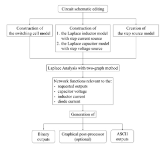 Figure 2: Block diagram of SapWinPE.
It is important to highlight that the network functions obtained by the program, and therefore by the described method, are not useful for a frequency-domain simulation, because the switch and diode models are not the same used to derive an averaged small-signal equivalent circuit of the switching cell. Note that a frequency domain analysis, resulting in bode plots and poles and zeros diagrams, can be performed by replacing the switching cell with time-invariant equivalent circuits as those presented in [38-45], which are different from those described in Section 2.
To suitably size the component values and evaluate the parasitic element effects during the design phase, it is possible to run a parametric analysis, one of the options of SapWinPE. Since parasitic components highly affect the converter dynamic behavior, multiparametric analysis provided by the program can be advantageously used to design the compensation network and investigate the stability of the converter when operated in closed loop.
The program also allows for multiple outputs, which result useful for a better understanding of the converter behavior. To this aim the knowledge of voltages in specific nodes and currents in different branches is crucial.
The semi-symbolic feature available in SapWinPE allows to better evaluate the effects of certain parameter variations by focusing on a few components, which are assumed as symbolic, while the others are set as numerical.
Note that the models described in Section 2 refer to ideal switches and diodes. By using ideal components, a fast, but inaccurate analysis of the circuit operation is achieved. For a better accuracy, parasitic elements can be externally added by the user. For example, some ringing in the current and voltage waveforms of a real converter are simply reproduced in the simulations by connecting to the ideal device appropriate parasitic components, affecting the operation of power MOSFETs and ultrafast or Schottky diodes. This allows accurate simulations to be executed by using data from component datasheet, while it is not necessary to know the physical operation of these devices. Of course, the higher is the number of added parasitic elements, the lower will be the processing speed.
Finally, to summarize the program steps, a block diagram of SapWinPE is shown in Figure 2.
5. Applications Examples
Figure 3(a) shows a buck converter including parasitic components as given by the SapWinPE schematic entry. In this section, the results of simulations run by using LTSpice are shown and compared with those achieved by using SapWinPE. In this circuit: RS is the power MOSFET ON resistance, Rd is the diode ON resistance, RL is the inductor equivalent series resistance (ESRL), and RC is the filter capacitor series resistance. An overall inductor equivalent series resistance can be derived as
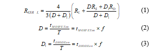 where f=1/T is the switching frequency. This resistance is series connected with the inductor, includes the parasitic resistances of the switching cell components, as shown in Figure 3(b), and simplifies the circuit analysis when a simulating tool is not available. Since in this paper we are using a power simulation program, the circuit shown in Figure 3(a) allows for a better insight of the circuit operation.
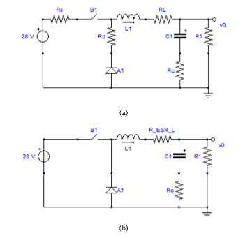 Figure 3: Buck converter including parasitic components. (a) Parasitic resistance for each component. (b) Parasitic resistance reduced to a single inductor equivalent series resistance R_ESR_L and to a capacitor parasitic resistance.
In the example, a buck converter designed according to the following specifications has been considered: output power PO = 10 W, input voltage VI = 28 V, load output voltage VO = 21 V, load resistance R = 3.6 W, switching frequency f = 40 kHz. Under these specifications, an inductance L = 3.3 mH has been designed, a filter capacitor C = 470 mF has been chosen to keep the output voltage ripple below 5%. The converter results to be operated at D = 0.036, and the parasitic components, as derived from component data sheets, are rS = 3 mW, rd = 20 mW, rL = 24 mW, and rC = 6 mW.
Figures 4(a) and 4(b) show the controlled switch and diode current waveforms as obtained by running simulations with LTSPice and SapWinPE, respectively. The plots show that the results obtained by using SapWinPE are nearly the same as those obtained with LTSpice.
The output voltage plots as derived by using LTSpice and SapWinPE are shown in Figures 5(a) and 5(b), respectively. The transient waveforms are nearly the same, as well as the voltage ripple; the average steady-state output voltage resulting from LTSpice is 20.6 V and that resulting from SapWinPE is 20 V. The transfer functions of the examples shown in this paper have not been included for reasons of brevity. However, it is possible to consult them at the following web address: http://www.cirlab.unifi.it/p122.html .
The small differences in the considered values depend on the different way the components are modeled in the two programs: LTSpice bases its simulations on physical models of the Mosfet and diode, while SapWinPE considers these components as ideal switches and parasitic resistances are added as external components in the simulated circuit.
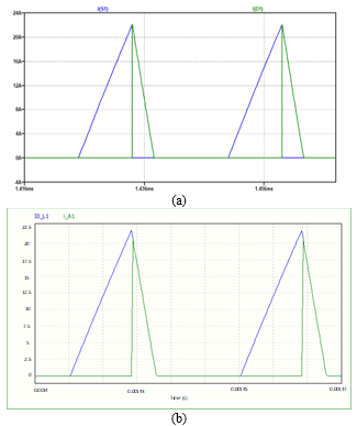 Figure 4: Buck converter current waveforms: power Mosfet current and diode current. (a) Plot resulting from LTSpice. (b) Plot resulting from SapWinPE.
Also, a PWM DC-DC buck-boost converter has been simulated and experimentally tested. The converter component values are as follows: inductance L = 224.62 µH, and its ESR is rL = 0.023 Ω, the capacitance is C = 662.32 µF, and its ESR is rC = 0.016 Ω. The power switch is constituted by a SCT3022AL SiC power Mosfet, which results in a breakdown voltage VDS = 650 V and a channel resistance rS = 22 mΩ. Finally, an FFSP2065B SiC diode has been utilized: it has a reverse voltage VR = 650 V, a threshold voltage VF =1.7 V, a continuous rectified forward current IF = 20 A, and a forward resistance rD = 33 mW. The input voltage is VI = 17 V, the output voltage is VO = 25 V, the duty cycle is D = 0.59, and the switching frequency is f = 20 kHz.
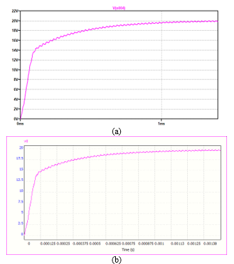 Figure 5: Output voltage ripple. (a) Plot resulting from LTSpice. (b) Plot resulting from SapWinPE.
Figure 6(a) shows the circuit of the buck-boost converter, as given by the SapWinPE schematic entry, which also includes: the MOSFET output capacitance Cds = 5 pF and inductance Ld = 100 nH, which considers parasitic inductances related to the layout of the experimentally tested circuit, shown in Figure 6(b) [46]. Figures 7(a) and (b) show the diode voltage waveforms resulting from the simulations and the experimental tests, respectively. The experimental waveform is plotted with a 10 ms/div time base and 10 V/div amplitude base.
The plots shown in Figure 7 clearly demonstrate that the simulated results are in good agreement with those experimentally measured. This confirms that SapWinPE results in accurate simulations of power converters, allows each parasitic component of the real circuit to be singularly considered, and, therefore, the user has a very good insight of the studied circuit.
6. New Approach
A new approach to the symbolic analysis of DC-DC converters has been conceived by the authors. The idea is to simulate DC-DC converters through the state variable method, suitable to analyze nonlinear circuits, as converters are. The network functions, determined as in the previous method in the Laplace domain and depending on initial conditions and switch and diode parameters, are relevant to the desired outputs and the converter state variables, that is inductor currents and capacitor voltages. The difference consists in the fact that switches and diodes are represented by parameters depending on analytical expressions reproducing the actual characteristics of these elements. The possibility of easily dealing with nonlinear components is linked with the adopted technique of inverse Laplace transform. It is executed in a discrete way, as the previous method, by using a very small sampling step, carefully chosen on the base of the specific case.
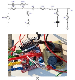 Figure 6: Buck-boost converter. a) Simulated circuit including parasitic components. b) Experimentally tested circuit.
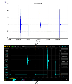 Figure 7: Waveforms of the buck-boost diode voltage. (a) Simulated. (b) Measured.
Each sample of the corresponding discretized impulsive response is multiplied by the input value in the sampling instant, so applying a discretized convolution integral for determining, point by point, the time domain response. Also in this case, not only the desired outputs are determined, but also the state variables in the time domain in each sampling step, because their values are necessary for correctly evaluating the desired outputs. The plot of the obtained response is determined by interpolating the output samples.
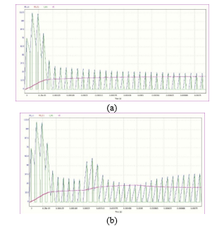 Figure 8. (a) Buck converter circuit simulation (inductor current IO_L1, capacitor voltage VO_C1, diode current i_A1, and output voltage VO) without parameters variation. (b) Buck converter circuit simulation: the duty cycle goes from 0.36 to 0.7 for t=0.25 ms, the resistor R1 goes from 3.6 Ω to 1 Ω for t=0.5 ms.
In this way, it is very easy to treat nonlinear elements, because only their value in the sampling instants is significant.
Whatever input waveform can be used, because it is sampled and held during the sampling step, so resulting in a step function of constant amplitude. The possibility of using any input waveform allows considering harmonics and noise overlapping with the input signal.
The implementation of this approach is still raw. Figure 8 shows the time response of the buck converter of Figure 3, obtained with a sketch of the symbolic program based on this approach.
7. Conclusions
The purpose of this paper is to present a method for applying the Laplace transform to DC-DC converters for simulating this kind of circuits through symbolic techniques.
Time-domain analysis of power converters is performed through the derivation of the circuit network functions. This is achieved by deriving suitable models for both switches and diodes.
The proposed approach is suited to computationally efficient topological methods which allows also large circuits, as, for example, DC-AC inverters and AC-DC rectifiers, to be simulated in short times. A symbolic program, named SapWinPE, implementing the proposed approach is also presented.
This program ensures accurate and fast simulations of switching circuits. It runs in a stand-alone configuration and can provide its outputs also in formats compatible with commercial programs such as MATLAB.
Sap Win PE validity is demonstrated by the examples shown in the paper and by its successful application to power converter fault diagnosis and resonant converter design [47-51].
Finally, a new state variable-based analysis technique for symbolic simulation of DC-DC converters is briefly introduced. Even if still in an embryonic state, it is promising. The implementation of a program based on this technique is planned for the near future.
Conflict of Interest
The authors declare no conflict of interest.
- F. Grasso, A. Luchetta, S. Manetti, M.C. Piccirilli, “Symbolic Techniques in DC-DC Converter Simulation,” in 2019 IEEE 5th International forum on Research and Technology for Society and Industry (RTSI), IEEE: 248–253, 2019, doi:10.1109/RTSI.2019.8895579.
- R.W. Erickson, D. Maksimović, Fundamentals of Power Electronics, Springer US, Boston, MA, 2001, doi:10.1007/b100747.
- F. Grasso, S. Manetti, M.C. Piccirilli, A. Reatti, “A Laplace transform approach to the simulation of DC-DC converters,” International Journal of Numerical Modelling: Electronic Networks, Devices and Fields, e2618, 2019, doi:10.1002/jnm.2618.
- H. Ardi, A. Farakhor, A. Ajami, “Design, analysis and implementation of a buck–boost DC/DC converter,” IET Power Electronics, 7(12), 2902–2913, 2014, doi:10.1049/iet-pel.2013.0874.
- H.S.H. Chung, K.K. Tse, A. Ioinovici, “Computer-aided analysis of power electronic circuits by stepwise topological identification,” International Journal of Numerical Modelling: Electronic Networks, Devices and Fields, 10(5), 285–301, 1997, doi:10.1002/(SICI)1099-1204(199709/10)10:5<285::AID-JNM279>3.0.CO;2-U.
- K. Guesmi, A. Hamzaoui, “On the modelling of DC-DC converters: An enhanced approach,” International Journal of Numerical Modelling: Electronic Networks, Devices and Fields, 24(1), 36–57, 2011, doi:10.1002/jnm.759.
- A. Opal, J. Vlach, “Analysis and sensitivity of periodically switched linear networks,” IEEE Transactions on Circuits and Systems, 36(4), 522–532, 1989, doi:10.1109/31.92884.
- M.-D. Ker, C.-C. Yen, “New Transient Detection Circuit for On-Chip Protection Design Against System-Level Electrical-Transient Disturbance,” IEEE Transactions on Industrial Electronics, 57(10), 3533–3543, 2010, doi:10.1109/TIE.2009.2039456.
- V. Vorpérian, Fast Analytical Techniques for Electrical and Electronic Circuits, Cambridge University Press, 2002, doi:10.1017/CBO9780511613791.
- D. Biolek, “Modeling of periodically switched networks by mixed s-z description,” IEEE Transactions on Circuits and Systems I: Fundamental Theory and Applications, 44(8), 750–758, 1997, doi:10.1109/81.611272.
- D. Biolek, V. Biolkova, J. Dobes, “Modeling of switched DC-DC converters by mixed s-z description,” in 2006 IEEE International Symposium on Circuits and Systems, IEEE: 4, doi:10.1109/ISCAS.2006.1692714.
- D. Biolek, V. Biolkova, Z. Kolka, “Analysis of switching effects in DC-DC converters via bias point computation,” in 2007 18th European Conference on Circuit Theory and Design, IEEE: 1006–1009, 2007, doi:10.1109/ECCTD.2007.4529769.
- F. Huliehel, S. Ben-Yaakov, “Low-frequency sampled-data models of switched mode DC-DC converters,” IEEE Transactions on Power Electronics, 6(1), 55–61, 1991, doi:10.1109/63.65003.
- C. Fang, E.H. Abed, “Output regulation of DC-DC switching converters using discrete-time integral control,” in Proceedings of the 1999 American Control Conference (Cat. No. 99CH36251), IEEE: 1052–1056 vol.2, 1999, doi:10.1109/ACC.1999.783201.
- D.M. Van de Sype, K. De Gusseme, A.R. Van den Bossche, J.A. Melkebeek, “Small-signal z-domain analysis of digitally controlled converters,” in 2004 IEEE 35th Annual Power Electronics Specialists Conference (IEEE Cat. No.04CH37551), IEEE: 4299–4305, doi:10.1109/PESC.2004.1354761.
- D. Maksimovic, R. Zane, “Small-signal Discrete-time Modeling of Digitally Controlled DC-DC Converters,” in 2006 IEEE Workshops on Computers in Power Electronics, IEEE: 231–235, 2006, doi:10.1109/COMPEL.2006.305680.
- L. Corradini, P. Mattavelli, “Analysis of Multiple Sampling Technique for Digitally Controlled dc-dc Converters,” in 37th IEEE Power Electronics Specialists Conference, IEEE: 1–6, doi:10.1109/PESC.2006.1712132.
- A.R. Brown, R.D. Middlebrook, “Sampled-data modeling of switching regulators,” in 1981 IEEE Power Electronics Specialists Conference, IEEE: 349–369, 1981, doi:10.1109/PESC.1981.7083659.
- G.C. Verghese, M.E. Elbuluk, J.G. Kassakian, “A General Approach to Sampled-Data Modeling for Power Electronic Circuits,” IEEE Transactions on Power Electronics, PE-1(2), 76–89, 1986, doi:10.1109/TPEL.1986.4766286.
- D.M. Van de Sype, K. De Gusseme, A.P. Van den Bossche, J.A. Melkebeek, “Small-signal Laplace-domain analysis of uniformly-sampled pulse-width modulators,” in 2004 IEEE 35th Annual Power Electronics Specialists Conference (IEEE Cat. No.04CH37551), IEEE: 4292–4298, doi:10.1109/PESC.2004.1354760.
- D. Maksimovic, R. Zane, “Small-Signal Discrete-Time Modeling of Digitally Controlled PWM Converters,” IEEE Transactions on Power Electronics, 22(6), 2552–2556, 2007, doi:10.1109/TPEL.2007.909776.
- M.M. Peretz, S. Ben-Yaakov, “Time-Domain Design of Digital Compensators for PWM DC-DC Converters,” IEEE Transactions on Power Electronics, 27(1), 284–293, 2012, doi:10.1109/TPEL.2011.2160358.
- M. Shirazi, J. Morroni, A. Dolgov, R. Zane, D. Maksimovic, “Integration of Frequency Response Measurement Capabilities in Digital Controllers for DC–DC Converters,” IEEE Transactions on Power Electronics, 23(5), 2524–2535, 2008, doi:10.1109/TPEL.2008.2002066.
- M.M. Peretz, S. Ben-Yaakov, “Time Domain Identification of PWM Converters for Digital Controllers Design,” in 2007 IEEE Power Electronics Specialists Conference, IEEE: 809–813, 2007, doi:10.1109/PESC.2007.4342092.
- A. Massarini, U. Reggiani, M.K. Kazimierczuk, “Analysis of networks with ideal switches by state equations,” IEEE Transactions on Circuits and Systems I: Fundamental Theory and Applications, 44(8), 692–697, 1997, doi:10.1109/81.611264.
- W. Pietrenko, W. Janke, M.K. Kazimierczuk, “Application of semianalytical recursive convolution algorithms for large-signal time-domain simulation of switch-mode power converters,” IEEE Transactions on Circuits and Systems I: Fundamental Theory and Applications, 48(10), 1246–1252, 2001, doi:10.1109/81.956022.
- F. Grasso, A. Luchetta, S. Manetti, M.C. Piccirilli, A. Reatti, “SapWin 4.0-a new simulation program for electrical engineering education using symbolic analysis,” Computer Applications in Engineering Education, 24(1), 44–57, 2016, doi:10.1002/cae.21671.
- W. Daems, G. Gielen, W. Sansen, “Circuit simplification for the symbolic analysis of analog integrated circuits,” IEEE Transactions on Computer-Aided Design of Integrated Circuits and Systems, 21(4), 395–407, 2002, doi:10.1109/43.992763.
- F. Fernandez, Á. Rodríguez-Vázquez, J.L. Huertas, G.G.E. Gielen, Symbolic Analysis Techniques, IEEE, 1998, doi:10.1109/9780470546512.
- P.M. Lin, Symbolic Network Analysis, Elsevier Science Ltd, New York, NY, USA, 1991. ISBN10 0444873899
- A. Ioinovici, “Generalised alternor,” Electronics Letters, 24(2), 122, 1988, doi:10.1049/el:19880081.
- A. Liberatore, A. Luchetta, S. Manetti, M.C. Piccirilli, “A new symbolic program package for the interactive design of analog circuits,” in Proceedings of ISCAS’95 – International Symposium on Circuits and Systems, IEEE: 2209–2212, doi:10.1109/ISCAS.1995.523866.
- L.P. Huelsman, “SapWin, symbolic analysis program for Windows — PC programs for engineers.,” IEEE Circuits and Devices Magazine, 12(6), 4–6, 1996.
- L.P. Huelsman, “Symbolic analysis-a tool for teaching undergraduate circuit theory,” IEEE Transactions on Education, 39(2), 243–250, 1996, doi:10.1109/13.502071.
- G. Fedi, R. Giomi, A. Luchetta, S. Manetti, M.C. Piccirilli, “SapWin 2.0: a symbolic software tool for educational purposes in analysis and synthesis of analog circuits,” in Proceedings of International Conference on Simulation and Multimedia in Engineering Education, ICSSE’99, San Francisco, CA: 33–36, 1999.
- J.B. Grimbleby, “Algorithm for finding the common spanning trees of two graphs,” Electronics Letters, 17(13), 470, 1981, doi:10.1049/el:19810328.
- K. Singhal, J. Vlach, Computer Methods for Circuit Analysis and Design, Springer-Verlag US, 1993.
- J. Sun, D.M. Mitchell, M.F. Greuel, P.T. Krein, R.M. Bass, “Averaged modeling of PWM converters operating in discontinuous conduction mode,” IEEE Transactions on Power Electronics, 16(4), 482–492, 2001, doi:10.1109/63.931052.
- A. Luchetta, S. Manetti, M.C. Piccirilli, A. Reatti, M.K. Kazimierczuk, “Comparison of DCM operated PWM DC-DC converter modelling methods including the effects of parasitic components on duty ratio constraint,” in 2015 IEEE 15th International Conference on Environment and Electrical Engineering (EEEIC), IEEE: 766–771, 2015, doi:10.1109/EEEIC.2015.7165261.
- A. Luchetta, S. Manetti, M.C. Piccirilli, A. Reatti, M.K. Kazimierczuk, “Effects of parasitic components on diode duty cycle and small-signal model of PWM DC-DC buck converter in DCM,” in 2015 IEEE 15th International Conference on Environment and Electrical Engineering (EEEIC), IEEE: 772–777, 2015, doi:10.1109/EEEIC.2015.7165262.
- A. Luchetta, S. Manetti, M.C. Piccirilli, A. Reatti, M.K. Kazimierczuk, “Derivation of network functions for PWM DC-DC Buck converter in DCM including effects of parasitic components on diode duty-cycle,” in 2015 IEEE 15th International Conference on Environment and Electrical Engineering (EEEIC), IEEE: 778–783, 2015, doi:10.1109/EEEIC.2015.7165263.
- A. Davoudi, J. Jatskevich, P.L. Chapman, “Averaged modelling of switched-inductor cells considering conduction losses in discontinuous mode,” IET Electric Power Applications, 1(3), 402, 2007, doi:10.1049/iet-epa:20060329.
- J. Sun, “Unified averaged switch models for stability analysis of large distributed power systems,” in APEC 2000. Fifteenth Annual IEEE Applied Power Electronics Conference and Exposition (Cat. No.00CH37058), IEEE: 249–255, doi:10.1109/APEC.2000.826112.
- D.K. Saini, A. Reatti, M.K. Kazimierczuk, “Average current-mode control of buck dc-dc converter with reduced control voltage ripple,” in IECON 2016 – 42nd Annual Conference of the IEEE Industrial Electronics Society, IEEE: 3270–3275, 2016, doi:10.1109/IECON.2016.7793204.
- A. Ayachit, A. Reatti, M.K. Kazimierczuk, “Small-signal modeling of PWM dual-SEPIC dc-dc converter by circuit averaging technique,” in IECON 2016 – 42nd Annual Conference of the IEEE Industrial Electronics Society, IEEE: 3606–3611, 2016, doi:10.1109/IECON.2016.7793030.
- P. Bernardi, R. Cicchetti, G. Pelosi, A. Reatti, S. Selleri, and M. Tatini, “An Equivalent Circuit for EMI Prediction in Printed Circuit Boards Featuring a Straight-to-Bent Microstrip Line Coupling,” Progress In Electromagnetics Research B, Vol. 5, 107-118, 2008. doi:10.2528/PIERB08020502
- A. Reatti, S. Manetti, M. C. Piccirilli, A. Luchetta and M. K. Kazimierczuk, “Multilayer neural network with multivalued neurons MLMVN based CLASS E resonant inverter fault detection,” 8th IET International Conference on Power Electronics, Machines and Drives (PEMD 2016), Glasgow, 2016, 1-6, doi: 10.1049/cp.2016.0265.
- M. Catelani, L. Ciani, A. Luchetta, S. Manetti, M.C. Piccirilli, A. Reatti, M.K. Kazimierczuk, “MLMVNN for parameter fault detection in PWM DC-DC converters and its applications for buck DC-DC converter,” in 2016 IEEE 16th International Conference on Environment and Electrical Engineering (EEEIC), IEEE: 1–6, 2016, doi:10.1109/EEEIC.2016.7555877.
- M. Catelani, L. Ciani, A. Luchetta, S. Manetti, M.C. Piccirilli, A. Reatti, M.K. Kazimierczuk, “Fault detection of resonant inverters for wireless power transmission using MLMVNN,” in 2016 IEEE 2nd International Forum on Research and Technologies for Society and Industry Leveraging a better tomorrow (RTSI), IEEE: 1–5, 2016, doi:10.1109/RTSI.2016.7740639.
- L. Albertoni, F. Grasso, J. Matteucci, M.C. Piccirilli, A. Reatti, A. Ayachit, M.K. Kazimierczuk, “Analysis and design of full-bridge Class-DE inverter at fixed duty cycle,” in IECON 2016 – 42nd Annual Conference of the IEEE Industrial Electronics Society, IEEE: 5609–5614, 2016, doi:10.1109/IECON.2016.7793240.
- F. Corti, F. Grasso, A. Reatti, A. Ayachit, D.K. Saini, M.K. Kazimierczuk, “Design of class-E ZVS inverter with loosely-coupled transformer at fixed coupling coefficient,” in IECON 2016 – 42nd Annual Conference of the IEEE Industrial Electronics Society, IEEE: 5627–5632, 2016, doi:10.1109/IECON.2016.7793285.
No related articles were found.