Applications of TCAD Simulation Software for Fabrication and study of Process Variation Effects on Threshold Voltage in 180nm Floating-Gate Device

Adv. Sci. Technol. Eng. Syst. J. 6(1), 146–152 (2021);
 DOI: 10.25046/aj060116
In this work, a study of the process variation effects on the threshold voltage of a floating- gate device is proposed. The study demonstrates the sensitivity of the threshold voltage to five geometrical parameters including gate length, gate width, tunneling gate oxide thickness, bottom oxide-nitride-oxide oxide thickness, and nitride spacer thickness. This paper also proposed a detailed flow to fabricate the floating-gate device for CMOS 180nm process, which is used to design the floating-gate device for the study. This paper used the TCAD tools including Athena, Devedit3D, and Atlas for the simulations.
1. Introduction
In this work, a detailed design flow and parameter values to fabricate the complete floating-gate device are proposed to investigate the structure and characteristics of the device. The process variation effects on the threshold voltage, which is a vital parameter of the device, are studied by using the TCAD simulation tools. Authors introduced the floating-gate device and presented ideas about how to study the process variation on threshold voltage in 180nm floating-gate device in the ”2019 19th International Symposium on Communications and Information Technologies (ISCIT)” [1] and the following paper is an extension of this work.
The remainder of this paper is organized as follows: Section II introduces an overview structure of the device in fabrication and the operation states also. Following this, the detailed flow and parameter values to fabricate a complete device are shown in section III. Next, section IV shows the analysis and discussion of the process variation results in the threshold voltage. This section also describes the simulation of operation states after fabricating. Finally, section V shows the conclusion.
2. Floating Gate Device
The floating-gate device is the core of almost modern non-volatile memories [20], [21]. With regards to fabrication, the device is recognized through the use of a ”floating gate”. The gate is completely surrounded by dielectrics [22]. A cross section of a device is given in Figure. 1. Being electrically isolated, the floating gate acts as the storing layer in the device. Therefore, the operation states of the device would be determined based on the status of the gate. More importantly, the insulator around the floating gate must be thick enough to prevent leakage of charges from the floating gate to the substrate when the power is off, and it also must be thin enough to allow the transfer of charges on and off the gate under appropriate bias configuration. Moreover, reducing the thickness of the insulator, especially the tunneling gate oxide thickness has been investigated to reduce the program/erase voltage and enhance the level of integration [13],[23].
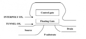
Figure 1: Floating-gate device structure in fabrication
The floating-gate device has three operation states which are programming, erasing, and reading. Programming refers to putting electrons called Channel Hot Electrons on the floating gate. In contrast, removing the electrons from the gate to the substrate would be performed in the erasing process. The removing current is renowned for the Fowler-Nordheim Tunnel current. Reading is used to determine if the device is programmed or erased.
3. Floating Gate Fabrication & Simulation
This flow proposes using an additional Epitaxial grow layer which was not used in traditional CMOS processes. The growth of an epitaxial layer over the P-type substrate offers some advantages including improving the performance of this device as well as floating-gate integrated circuits, minimizing latch-up effects that a CMOS circuit may undergo when powered up, and helping control the doping concentration of this device accurately [24].

Figure 2: Floating-gate device design flow chart
The main difference in terms of structure between the floatinggate device and CMOS device is that the former has an additional floating gate which is created by two steps (Deposit Polysilicon (Floating gate), Dope Polysilicon (Floating gate) in the flow. These figures below illustrate the main process simulations using TCAD based on the design flow chart presented above (Figure 3a-3h).
The fabrication process starts from creating P-substrate (initial surface thickness = 1µm) with Boron at a concentration of 1.0e14 cm−3 (Figure 3a). Next, a mesh is defined, and the density of the mesh is a trade-off between accuracy and simulation time. After the mesh and wafer definition, a 0.45µm thick Epitaxy layer with Arsenic at a concentration of 1.0e16 cm−3 is grown on the top to make device surface thickness increase to 1.45µm (Figure 3b). Then, a P well is implanted using Boron with a dose of 8e12 cm−3. After that, the P well is also diffused with Nitro gas at 12000C for about 310 minutes (Figure 3c). Next, Locos and tunnel oxide layer are created (Figure 3d). Creating Locos is an important step in the fabrication of semiconductor devices for the purpose of isolating the operation of two devices on the same wafer, and Oxide is usually used for this isolation. The doping channel is created using Boron at 100KeV and a concentration of 2.5e12 cm−3 (Figure 3e). Figure 3f shows the device structure after Polysilicon (Floating gate) is deposited and doped. Figure 3g shows the device structure after Polysilicon (Control gate) is deposited and doped. The Floating gate, Control gate, Tunnel Oxide layer and Oxide-Nitride-Oxide layer which is between Floating gate and Control gate are etched. An oxide layer with a thickness of 0.1µm is deposited and etched on the top to protect the device by the next steps. The next step is to create Source and Drain gates with Arsenic at 50 KeV and a concentration of

Figure 3: The main process simulations with TCAD including in a) Definition wafer b) Grow Epitaxial layer c) P well drive d) After creating Locos and grow Gate oxide e) Dope channel f) Create Floating gate and dope polysilicon g) Create Control gate and dope polysilicon h) After implant and diffuse S/D dopants 7e12 cm−3 (Figure 3h). After growing the protection layer, the final step is to deposit and etch Aluminum contacts for Source and Drain gates. The detailed process flow to fabricate the device is presented in Figure 2.
In this work, we propose to use the Athena tool to simulate the process of fabrication and the Atlas tool for operation simulations of the device. The following table gives the default parameter values in designing.
Table 1: Description And Default Parameter Values
| DESCRIPTION | VALUE [µm] |
| Thickness of oxide-nitride-oxide nitride | 0.013 |
| Thickness of nitride spacer | 0.002 |
| Thickness of bottom oxide-nitride-oxide oxide | 0.01 |
| Thickness of top oxide-nitride-oxide oxide | 0.001 |
| Thickness of tunneling gate oxide | 0.02 |
| Thickness of control gate | 0.075 |
| Thickness of floating gate | 0.075 |
| Length of control gate | 0.18 |
| Length of floating gate | 0.18 |
The complete 2D and 3D structures of the device in this work are given in Fig. 4 and Fig. 5, respectively. Regarding the 3D structure, the one is designed by using the 2D structure and the Devedit3D tool.

Figure 4: The 2D floating-gate device structure
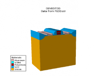
Figure 5: The 3D floating-gate device structure
4. Process Variation Results
This section presents the threshold voltage results of the floatinggate device designed in the previous section before programming and after programming.
Initially, before programming, there are no charges which are stored on the floating gate. The drain current – threshold voltage curve is shown in Fig. 6. The threshold voltage of the device is 0.6V.
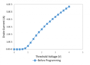
Figure 6: Threshold voltage of the device before programming process
After the programming process, the charges on the gate increase from 0C to around -3.5e-15C since the moving of electrons from the substrate. Meanwhile, the threshold voltage increases from 0.6V to approximately 6V. The charges on the gate and the threshold voltage in the programming process are given in Fig. 7 and Fig. 8, respectively. After that, the device is at the program state.
In contrast, as discussed in section II, the erasing process will remove all the negative charge on the floating gate which is generated from the programming process. Following this, the floating gate will have no charge, and the state of the device is as the initial (before programming state) or erasing state.
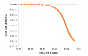
Figure 7: Floating gate charge in the programming process
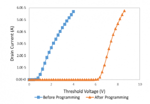
Figure 8: Threshold voltage of the device after programming process
The study of process variation demonstrates the effect of the threshold voltage on different geometrical parameters. In general, what stands out from the study is that whereas the threshold voltage is more sensitive to the gate length, tunneling gate oxide thickness, and bottom oxide-nitride-oxide oxide thickness, the threshold voltage is less sensitive to the gate width and nitride spacer thickness. The details of the study are given as follows.
4.1 Vary in values of the gate length
The figure in this section demonstrates the effect of the gate length parameter on the threshold voltage, it is clear that the increase in this parameter tends to a considerable increase in the threshold voltage, climbing around 18.33%, from 6V to approximately 7.1V. Thus, in the fabrication process, this parameter should be controlled carefully.
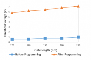
Figure 9: Gate length variation effects
4.2 Vary in values of the gate width
The figure below illustrates the change of the threshold voltage when the width parameter changes from 0.4µm to 1.6µm. This parameter is defined as a variable varied in the z-axis of the Devedit3D tool. In general, what stands out from the graph is that the voltage is not sensitive to this parameter. The threshold voltage remains stable at around 6V.

Figure 10: Gate width variation effects
4.3 Vary in values of the tunneling gate oxide thickness
The result is given in the graph in Fig. 11, it is clear that the change in tunneling gate oxide thickness results in a dramatic decrease in the threshold voltage when it varies from 20nm to 40nm. After programming, the voltage witnessed a drastic decrease, falling approximately 50% to about 3.2V. Hence, this is a very important parameter because the variation of the one causes a significant change in the operation of the device. With regard to the fabrication process, this parameter should be controlled carefully.
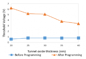
Figure 11: Tunneling gate oxide thickness variation effects
4.4 Vary in values of the bottom oxide-nitride-oxide oxide thickness
The graph in this section shows the results of the threshold voltage when the bottom oxide-nitride-oxide oxide thickness varied from 0.01µm to 0.03µm. Overall, it can be seen that the threshold voltage after programming experienced a considerable decrease of 23.33%, dropping from roughly 6V to approximately 4.6V. Thus, in the fabrication process, similar to the gate length and the tunneling gate oxide thickness, this parameter should be observed carefully.

Figure 12: Bottom oxide-nitride-oxide oxide thickness variation effects
4.5 Vary in values of the nitride spacer thickness
The graph in the Fig. 13 presents the impact of the nitride spacer thickness parameter on the threshold voltage. It is clear that the impact of this parameter is very small. The threshold voltage after programming remaining between 5.9V and 6.1V throughout the study. Thus, the parameter would be controlled more easily than the others in the fabrication process.
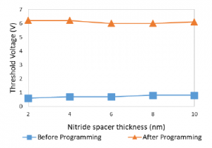
Figure 13: Nitride spacer thickness variation effects
5. Conclusion
This work is successful in the study of the process variation effects on the performance of a floating-gate device. The tunneling gate oxide thickness, bottom oxide-nitride-oxide oxide thickness, and gate length were found out to be sensitive to the threshold voltage, especially the tunneling gate oxide thickness parameter caused 50% change in threshold voltage. The others are 18.33% and 23.33%, respectively. While the gate width, nitride spacer thickness turned out to be less sensitive. This paper also successful in proposing a detailed flow and the parameter values to fabricate the complete floating-gate device based on CMOS 180nm process. The device which is designed by the flow worked as the expectation.
Conflict of Interest
The authors declare no conflict of interest.
Acknowledgment
This research is funded by Ho Chi Minh City University of Technology (HCMUT), VNU-HCM, under grant number BK-SDH-20212080912.
- T. D. Cong, T. Le Thanh, H. M. Tri, T. Hoang, “The Simulation Study of Process Variation on Threshold Voltage in 180nm Floating-Gate device,” in 2019 19th International Symposium on Communications and Information Technologies (ISCIT), 211–214, 2019, doi:10.1109/ISCIT.2019.8905125.
- R. B. Wunderlich, F. Adil, P. Hasler, “Floating Gate-Based Field Programmable Mixed-Signal Array,” IEEE Transactions on Very Large Scale Integration (VLSI) Systems, 21(8), 1496–1505, 2013, doi:10.1109/TVLSI.2012.2211049.
- T. Kim, K. Park, T. Jang, M.-H. Baek, Y. S. Song, B.-G. Park, “Input- modulating adaptive neuron circuit employing asymmetric floating-gate MOS- FET with two independent control gates,” Solid-State Electronics, 163, 107667, 2020, doi:https://doi.org/10.1016/j.sse.2019.107667.
- X. He, X. Zhu, L. Duan, Y. Sun, C. Ma, “A 14-mW PLL-Less Receiver in 0.18- µm CMOS for Chinese Electronic Toll Collection Standard,” IEEE Trans- actions on Circuits and Systems II: Express Briefs, 61(10), 763–767, 2014, doi:10.1109/TCSII.2014.2345303.
- J. Sun, C. C. Boon, X. Zhu, X. Yi, K. Devrishi, F. Meng, “A Low- Power Low-Phase-Noise VCO With Self-Adjusted Active Resistor,” IEEE Microwave and Wireless Components Letters, 26(3), 201–203, 2016, doi: 10.1109/LMWC.2016.2521167.
- H. Liu, C. C. Boon, X. He, X. Zhu, X. Yi, L. Kong, M. C. Heimlich, “A Wide- band Analog-Controlled Variable-Gain Amplifier With dB-Linear Characteris- tic for High-Frequency Applications,” IEEE Transactions on Microwave Theory and Techniques, 64(2), 533–540, 2016, doi:10.1109/TMTT.2015.2513403.
- H. Liu, X. Zhu, C. C. Boon, X. He, “Cell-Based Variable-Gain Ampli- fiers With Accurate dB-Linear Characteristic in 0.18 µm CMOS Technol- ogy,” IEEE Journal of Solid-State Circuits, 50(2), 586–596, 2015, doi: 10.1109/JSSC.2014.2368132.
- X. Tong, Y. Yang, Y. Zhong, X. Zhu, J. Lin, E. Dutkiewicz, “Design of an On-Chip Highly Sensitive Misalignment Sensor in Silicon Technology,” IEEE Sensors Journal, 17(5), 1211–1212, 2017, doi:10.1109/JSEN.2016.2638438.
- S. Chakraborty, Y. Yang, X. Zhu, O. Sevimli, Q. Xue, K. Esselle, M. Heimlich, “A Broadside-Coupled Meander-Line Resonator in 0.13- µm SiGe Technol- ogy for Millimeter-Wave Application,” IEEE Electron Device Letters, 37(3), 329–332, 2016, doi:10.1109/LED.2016.2520960.
- G. O. Puglia, A. F. Zorzo, C. A. F. De Rose, T. Perez, D. Milojicic, “Non- Volatile Memory File Systems: A Survey,” IEEE Access, 7, 25836–25871, 2019, doi:10.1109/ACCESS.2019.2899463.
- E. I. Vatajelu, H. Aziza, C. Zambelli, “Nonvolatile memories: Present and fu- ture challenges,” in 2014 9th International Design and Test Symposium (IDT), 61–66, 2014, doi:10.1109/IDT.2014.7038588.
- R. Bez, E. Camerlenghi, A. Modelli, A. Visconti, “Introduction to flash mem- ory,” Proceedings of the IEEE, 91(4), 489–502, 2003, doi:10.1109/JPROC. 2003.811702.
- S. Wang, C. He, J. Tang, X. Lu, C. Shen, H. Yu, L. Du, J. Li, R. Yang, D.-X. Shi, G. Zhang, “Nonvolatile Memory: New Floating Gate Memory with Ex- cellent Retention Characteristics (Adv. Electron. Mater. 4/2019),” Advanced Electronic Materials, 5, 2019, doi:10.1002/aelm.201970018.
- E.-J. Park, J.-M. Choi, K.-W. Kwon, “Behavior Modeling for Charge Storage in Single-Poly Floating Gate Device,” Journal of nanoscience and nanotechnology, 19, 6727–6731, 2019, doi:10.1166/jnn.2019.17112.
- L. L. M. A. Pavan, Paolo, Floating Gate Devices: Operation and Compact Modeling, Springer US, 2004.
- G. Rappitsch, E. Seebacher, M. Kocher, E. Stadlober, “SPICE modeling of process variation using location depth corner models,” IEEE Transactions on Semiconductor Manufacturing, 17(2), 201–213, 2004, doi:10.1109/TSM.2004. 826940.
- F. Duvivier, E. Guichard, “Worst-case SPICE model generation for a process in development using Athena, Atlas, Utmost and Spayn,” in ICM 2001 Proceed- ings. The 13th International Conference on Microelectronics., 11–18, 2001, doi:10.1109/ICM.2001.997475.
- Y. Saad, C. Tavernier, M. Ciappa, W. Fichtner, “TCAD tools for efficient 3D simulations of geometry effects in floating-gate structures,” in Proceedings. 2004 IEEE Computational Systems Bioinformatics Conference, 77–82, 2004, doi:10.1109/NVMT.2004.1380810.
- S. Bala, B. Mahendia, “Simulation of Floating Gate MOSFET Using Silvaco TCAD Tools,” 2015.
- S. Agarwal, D. Garland, J. Niroula, R. B. Jacobs-Gedrim, A. Hsia, M. S. Van Heukelom, E. Fuller, B. Draper, M. J. Marinella, “Using Floating-Gate Memory to Train Ideal Accuracy Neural Networks,” IEEE Journal on Ex- ploratory Solid-State Computational Devices and Circuits, 5(1), 52–57, 2019, doi:10.1109/JXCDC.2019.2902409.
- T. Dubey, V. Bhadauria, “A low-voltage highly linear OTA using bulk-driven floating gate MOSFETs,” AEU – International Journal of Electronics and Com- munications, 98, 2018, doi:10.1016/j.aeue.2018.10.034.
- P. Pavan, R. Bez, P. Olivo, E. Zanoni, “Flash memory cells-an overview,” Proceedings of the IEEE, 85(8), 1248–1271, 1997, doi:10.1109/5.622505.
- R. Dhavse, F. Muhammed, C. Sinha, V. Mishra, R. M. Patrikar, “Memory characteristics of a 65 nm FGMOS capacitor with Si quantum dots as float- ing gates,” in 2013 Annual IEEE India Conference (INDICON), 1–3, 2013, doi:10.1109/INDCON.2013.6725910.
- R. N. T. Stanley Wolf, Silicon Processing for the VLSI Era, Volume1: Process Technology, Lattice Press; 1st edition (January 1, 1986), 1999.
No related articles were found.