
A Novel Approach to Design a Process Design Kit Digital for CMOS 180nm Technology
Volume 6, Issue 1, Page No 1191-1198, 2021
Author’s Name: Thinh Dang Cong1,2, Toi Le Thanh1,2, Phuc Ton That Bao1,2, Trang Hoang1,2,a)
View Affiliations
1Department of Electronics Engineering, Ho Chi Minh City University of Technology (HCMUT), Ho Chi Minh City, 72506, Vietnam
2Vietnam National University, Ho Chi Minh City, 71308, Vietnam
a)Author to whom correspondence should be addressed. E-mail: hoangtrang@hcmut.edu.vn
Adv. Sci. Technol. Eng. Syst. J. 6(1), 1191-1198 (2021); ![]() DOI: 10.25046/aj0601135
DOI: 10.25046/aj0601135
Keywords: Process Design Kit (PDK), Standard Cell Library (SCL), Liberty format, Wire-load Model (WLM), Ocean language

Export Citations
In this paper, a novel approach to design a Process Design Kit Digital for CMOS 180nm process is presented. This work proposes a detailed flow to design a PDK Digital using Ocean language, which is a vital element in the semi-custom design and applied in education purposes in universities in Vietnam. The PDK digital includes Standard Cell Library containing 47 standard cells and Wire-Load Model. The library is designed based on the CMOS 180nm process with a supply voltage of 1.8V.
Received: 08 December 2020, Accepted: 31 January 2021, Published Online: 25 February 2021
1. Introduction
CMOS technology has been developing in recent years due to its benefits such as high integration density, low fabrication cost, etc. Many new techniques of circuit design have been given ranging from RFIC [1]–[5] to mm-Wave IC design [6], [7].
In the past, the full custom design took many resources, efforts, and design time for designing a big chip. Meanwhile, the semi-custom design has significant decreased in the design and verification time for chip design by using the Electronic Design Automation (EDA) tools and PDK digital [8]. Especially, the latter provides a considerable decrease in design time, decreasing around 25% to 50%. Moreover, the latter would be applying for many more complex designs than the former [9].
Focusing on the PDK digital, the one consists of Synopsys library and P&R library [10]. While the former is applied for timing, power consumption, and noise analysis, the latter is used for place and route design in a design flow [11]. There are two ways to design an SCL. The first one uses the Liberty NCX tool of Synopsys. The Liberty NCX determines the function of standard cells. Following this, the tool creates the complete simulations by using HSPICE that would make the liberty file for each logic cell in the library [12], [13]. The second way performs characterization for all standard cells manually using the Spectre tool. The process of characterization consists of many simulations where the transition of the input and the capacitance of output load are varied. Timing and other parameters would be extracted, and outputted as a liberty format file.
The license of the Liberty NCX tool is unavailable at universities in developing countries due to its cost. Therefore, designing an SCL using this tool is almost impossible [13]. With regards to the manual characterization, the challenge is that we have to do many simulations to generate timing, power consumption, etc [14]. This way takes much time to design each logic cell. For instance, to design an INV logic cell, we have to do 7×7 simulations and 49×6 calculations to generate all parameters for the liberty file.
In this work, the Ocean language is proposed to solve problems about the licensing and running manually many simulations. The language is an extension of the Skill language used to control
Analog simulation. The flow automatically performs parametric simulations of each logic cell and generates output parameters with the format as the liberty file [15]. Regarding the Wire-Load Model (WLM), this paper proposed a method and used accuracy formulas to design a complete model.
The authors presented ideas about designing a PDK Digital for CMOS technology in the ”2019 19th International Symposium on Communications and Information Technologies (ISCIT)” [1] and the following paper is an extension of this work.
The remainder of this paper is organized as follows: Section II shows the SCL design flow from the transistor level. This section also gives the schematic design, Euler rules for layout design, DRC/LVS definition, etc. A detailed liberty format generation flow is given in section III. Section IV shows how to design a wire-load model. Finally, section V presents the conclusion.
2. Standard Cell Library Design
An SCL is made up of combinational logic cells such as INV, AND, FA, sequential logic cells such as DFF, Latch, and physical cells, etc. The design flow is composed of many steps. To begin with the front-end design stage, firstly, the schematic of all standard cells in the library are designed from transistor level. After that, symbol creation and do simulation at corners [16]. Next, in the back-end design stage, to optimize the layout design in term of area and routing, the layout design needs to have some rules as follows:
- All the input and output pins must be placed on the intersections of the vertical and horizontal routing tracks with the special exception for power and ground pins.
- All the cells in the library are designed to be multiple of the unit tile which is defined by a library developer. The height of the cells must be equal and be multiple of the unit tile’s height.
- This work uses M1 and M2 for the layout design.
- Minimize the width of all standard cells in the library.
- Optimize pins access to prevent the routing congestion in place and route stage.
- Some special cells such as filler, decap cells can be put in the library to make sure the connection of supply trails and N-well.
The figure below shows the schematic, Euler path for optimization, and layout design of an AOI22 cell in the library. The layout should follow the considerations as above.

Figure 1: a. Schematic design, b. Euler path, c. Layout design
The Physical Verification process will be performed after the layout design. This process will accomplish sequentially Design Rule Check (DRC) verification and Layout Versus Schematic (LVS) verification.
Firstly, by using the rules from the fabricators, the layout design is checked to ensure no potential violation, which is called DRC verification. The design rules are supplied by the manufacturers to ensure the chip will function properly when fabricated. The design rules include many rules such as the minimal critical dimensions, shape angles, pattern density requirements, etc [17]. The DRC flow chart is shown in Figure 2 and the example design rules are presented in Figure 3.
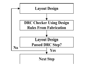
Figure 2: DRC flow chart
For example, the resolution rules for metal 1 and metal 2 layers are 0.23µm and 0.28µm, respectively. With regards to the rules for poly layer, the min.poly width is 0.18µm, min.gate to contact spacing is 0.375µm, and the min.poly overlap of diffusion is 0.22µm. For contact rules, the exact size and min.contact overlap are 0.22µm and 0.12µm, respectively.
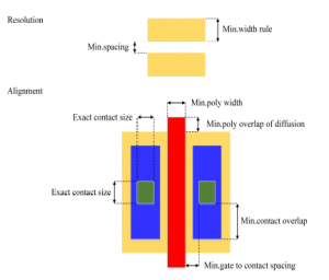
Figure 3: The example rules are used for DRC check
Followed by the LVS verification, which is the more critical verification step. Particularly, the LVS compares any combination of physical or schematic designs.
Depending on the layout design, so different parasitic components can be generated. These parasitic parameters can make the functionality and characteristic of the layout design different from schematic design. For that reason, if the whole parameters in the schematic design are different from the parasitic parameters of the layout design, which makes it impossible to complete the LVS step. Hence, this verification proves the chip after being fabricated will function as the schematic design [17]. When the LVS errors occur, we have to fix the layout design and perform the DRC step again to complete the LVS step without errors. The LVS flow chart is shown in Figure 4.
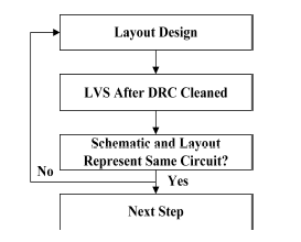
Figure 4: LVS flow chart
The Physical Verification process plays a vital role in the design flow. Therefore, the designers ensure that each cell in the library passed the DRC and LVS without any violations [18]. After the Physical Verification process, the post-layout simulation at corners will be executed before the cell characterization step. Next, Layout Parasitic Extraction (LPE) step is performed. Afterward, the postlayout simulations at corners are performed by using the parasitic parameters extracted. Therefore, the characterization of the standard cells will be calculated [19]. The post-layout simulation becomes possible and correct only after the LVS step is completed, then the extracted parameters are accurate. The post-layout simulation process will be shown in Figure 5.
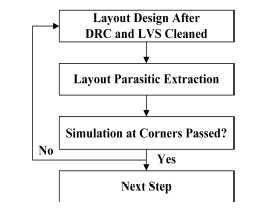
Figure 5: Post Layout Simulation Process Flow chart
Finally, the characterization step is divided into Liberty Format Generation step and Abstract View & GDS step. While the timing models, power models including dynamic and static power are extracted by the former to make the liberty file (*.lib) [20]. The Synopsys internal database format (*.db) may be translated from the liberty file by the Library Compile tool of Synopsys. The latter is used to create the library exchange format (*.lef) file by abstracting from the layout design, and the last step is the generating GDS file [21]. The block diagram in the figure below (Figure 6) illustrates the SCL design flow.

Figure 6: SCL design flow chart
3. Liberty Format Generation
After the post-layout simulation process, the standard cell characterization process is performed. Especially, the liberty format generation process, this process will generate an output file (*.lib) which is one of the most important files in the standard cell library design. The liberty file includes structural information, functional information, timing information, power information, and environmental information of each standard cell.
Firstly, the structural one declares connectivity of a logic cell including cell, bus, and in-out pin descriptions. Secondly, the functional one describes the logical function of each output pin of each cell. Thirdly, timing models are given including cell rise delay, cell fall delay, rise transition, fall transition. Next, power models give the dynamic and static power consumption of each cell. Finally, environmental information describes the manufacturing process, temperature of operation, supply voltage, etc.
In this part, to perform cell characterization and generate output file same as the liberty file’s format, all cells in the library will have the same load capacitance Cload = 2 fF, 5 fF, 6 fF, 7 fF, 8 fF, 9 fF, 9.5 fF, the input slew of the waveform slope = 0.01 ns, 0.02 ns, 0.04 ns, 0.06 ns, 0.08 ns, 0.09 ns, 0.095 ns [22]. The load capacitance and input slew are declared in the Ocean file to create 7×7 = 49 simulation times and extract the timing model and dynamic power consumption for each cell.
These figures below (Figure7 and Figure 8) show the testbench circuits for the Ocean script run and the results of a NAND gate cell with two inputs.

Figure 7: Testbench circuits for characterization

Figure 8: Waveform results
3.1 Input capacitance
In SCL design, one of the most important parameters that we need to calculate is input capacitance. The output capacitance of each cell can be determined but in most cases, the capacitance is specified only for the inputs and not for the outputs, which means that the output pin capacitance is zero in the library design [23].
The following formula illustrates the relationship between input capacitance, current, and supply voltage at an input pin.
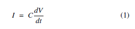
where I is the current at the input pin, V is the supply voltage and it is equal to 1.8V in this paper. By inputting a pulse power to the input pin and calculating the current, the input capacitance value is determined as the formula below:
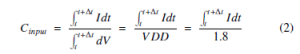
where ∆t is the time when the voltage at each input pin changes the logic level.
The two tables below show the capacitance of each input pin of the NAND2 cell. These tables also provide the rise power and fall power which are presented in the next section.
Table 1: PIN A
| tn(ns) | 0.01 | 0.02 | 0.04 | 0.06 | 0.08 | 0.09 | 0.095 |
| RISE POWER | 0.001098 | 0.001099 | 0.001101 | 0.001098 | 0.001100 | 0.001093 | 0.001097 |
| FALL POWER | 0.002029 | 0.002049 | 0.002053 | 0.002040 | 0.002044 | 0.002045 | 0.002044 |
| INPUT CAPACITANCE = 3.079fF | |||||||
Table 2: PIN B
| tn(ns) | 0.01 | 0.02 | 0.04 | 0.06 | 0.08 | 0.09 | 0.095 |
| RISE POWER | 0.001404 | 0.001406 | 0.001407 | 0.001405 | 0.001412 | 0.001409 | 0.001407 |
| FALL POWER | 0.001552 | 0.001534 | 0.001516 | 0.001504 | 0.001491 | 0.001483 | 0.001478 |
| INPUT CAPACITANCE = 2.774fF | |||||||
3.2 Timing models
All the timing arcs of the cell are declared in the timing model. There are two types of timing models that are linear and non-linear timing. Whereas the former provides less accurate for the submicron process, the latter is better. Therefore, most standard cell libraries use the latter. [20]. The definitions of all the timing arcs in the timing model are given in these figures as follows (Figure 9-11):
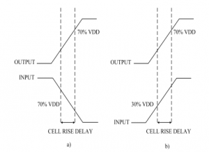
Figure 9: a. Cell rise delay at negative unate case, b. Cell rise delay at positive unate case
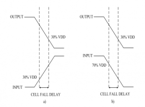
Figure 10: a. Cell fall delay at negative unate case, b. Cell fall delay at positive unate case

Figure 11: a. Rise transition time, b. Fall transition time
Table 3: Cell Rise Delay
| CloadPPPPtPnP | 0.01 | 0.02 | 0.04 | 0.06 | 0.08 | 0.09 | 0.095 |
| 2 | 0.0284388 | 0.0459522 | 0.0481537 | 0.0503347 | 0.0524551 | 0.0545356 | 0.0555650 |
| 5 | 0.0430937 | 0.0497589 | 0.0518424 | 0.0538036 | 0.0562515 | 0.0583046 | 0.0593685 |
| 6 | 0.0506982 | 0.0573539 | 0.0592578 | 0.0614723 | 0.0635472 | 0.0659118 | 0.0670066 |
| 7 | 0.0587234 | 0.0650961 | 0.0671953 | 0.0692366 | 0.0712060 | 0.0733503 | 0.0744634 |
| 8 | 0.0665493 | 0.0729249 | 0.0751495 | 0.0772798 | 0.0793351 | 0.0813871 | 0.0825202 |
| 9 | 0.0706249 | 0.0768656 | 0.0790399 | 0.0810872 | 0.0832540 | 0.0854972 | 0.0864483 |
| 9.5 | 0.0726732 | 0.0790870 | 0.0809977 | 0.0832278 | 0.0853940 | 0.0873195 | 0.0882354 |
Table 4: Cell Fall Delay
| CloadPPPPtPPn | 0.01 | 0.02 | 0.04 | 0.06 | 0.08 | 0.09 | 0.095 |
| 2 | 0.0352318 | 0.0874551 | 0.0911567 | 0.0954046 | 0.0996116 | 0.103758 | 0.105814 |
| 5 | 0.0779892 | 0.0903443 | 0.0936665 | 0.0979536 | 0.1021390 | 0.105976 | 0.108099 |
| 6 | 0.0836045 | 0.0958160 | 0.0996820 | 0.1035520 | 0.1078860 | 0.112125 | 0.114218 |
| 7 | 0.0899048 | 0.1018210 | 0.1061800 | 0.1103530 | 0.1144480 | 0.118486 | 0.120481 |
| 8 | 0.0966727 | 0.1086380 | 0.1126100 | 0.1169130 | 0.1210420 | 0.125246 | 0.127239 |
| 9 | 0.1002420 | 0.1123940 | 0.1164030 | 0.1203470 | 0.1240760 | 0.128452 | 0.130556 |
| 9.5 | 0.1019340 | 0.1139970 | 0.1181590 | 0.1222040 | 0.1261880 | 0.130108 | 0.131898 |
Table 5: Rise Transition
| CloadPPPPtPnP | 0.01 | 0.02 | 0.04 | 0.06 | 0.08 | 0.09 | 0.095 |
| 2 | 0.0285015 | 0.0525788 | 0.0565313 | 0.0590775 | 0.0617117 | 0.0643864 | 0.0657346 |
| 5 | 0.0444646 | 0.0525918 | 0.0556488 | 0.0590963 | 0.0622286 | 0.0641798 | 0.0666422 |
| 6 | 0.0454360 | 0.0532991 | 0.0566497 | 0.0593233 | 0.0623244 | 0.0653851 | 0.0665893 |
| 7 | 0.0483083 | 0.0564303 | 0.0588248 | 0.0616149 | 0.0644307 | 0.0672005 | 0.0683990 |
| 8 | 0.0519840 | 0.0593587 | 0.0620207 | 0.0648213 | 0.0673532 | 0.0702575 | 0.0715643 |
| 9 | 0.0544479 | 0.0608779 | 0.0637309 | 0.0668407 | 0.0693130 | 0.0715348 | 0.0725691 |
| 9.5 | 0.0554892 | 0.0626609 | 0.0649285 | 0.0673040 | 0.0697900 | 0.0727158 | 0.0742639 |
Table 6: Fall Transition
| CloadPPPPtPnP | 0.01 | 0.02 | 0.04 | 0.06 | 0.08 | 0.09 | 0.095 |
| 2 | 0.0294817 | 0.0918175 | 0.0966698 | 0.102074 | 0.107603 | 0.113067 | 0.115792 |
| 5 | 0.0765303 | 0.0921913 | 0.0968935 | 0.102306 | 0.107671 | 0.112408 | 0.115192 |
| 6 | 0.0763769 | 0.0914495 | 0.0964209 | 0.102027 | 0.107571 | 0.113009 | 0.115709 |
| 7 | 0.0763993 | 0.0916860 | 0.0970722 | 0.102287 | 0.107523 | 0.112521 | 0.115014 |
| 8 | 0.0779230 | 0.0930608 | 0.0984027 | 0.103380 | 0.108256 | 0.113244 | 0.115654 |
| 9 | 0.0789342 | 0.0936807 | 0.0983939 | 0.103534 | 0.108970 | 0.114131 | 0.116615 |
| 9.5 | 0.0800157 | 0.0946327 | 0.0993140 | 0.104174 | 0.108800 | 0.113987 | 0.116831 |
Table 7: Rise Power Consumption
|
PPP Cload |
tn PPP |
0.01 | 0.02 | 0.04 | 0.06 | 0.08 | 0.09 | 0.095 |
| 2 | -3.460e-05 | -5.033e-05 | -5.365e-05 | -5.692e-05 | -6.020e-05 | -6.348e-05 | -6.512e-05 | |
| 5 | -4.006e-05 | -5.040e-05 | -5.376e-05 | -5.703e-05 | -6.031e-05 | -6.351e-05 | -6.485e-05 | |
| 6 | -4.021e-05 | -5.025e-05 | -5.357e-05 | -5.691e-05 | -6.019e-05 | -6.347e-05 | -6.510e-05 | |
| 7 | -4.022e-05 | -5.011e-05 | -5.339e-05 | -5.680e-05 | -6.010e-05 | -6.329e-05 | -6.497e-05 | |
| 8 | -4.043e-05 | -5.025e-05 | -5.353e-05 | -5.673e-05 | -6.013e-05 | -6.327e-05 | -6.495e-05 | |
| 9 | -4.050e-05 | -5.033e-05 | -5.357e-05 | -5.686e-05 | -6.015e-05 | -6.342e-05 | -6.508e-05 | |
| 9.5 | -4.051e-05 | -5.030e-05 | -5.356e-05 | -5.685e-05 | -6.013e-05 | -6.350e-05 | -6.515e-05 |
Table 8: Fall Power Consumption
| CloadPPPPtPnP | 0.01 | 0.02 | 0.04 | 0.06 | 0.08 | 0.09 | 0.095 |
| 2 | -2.729e-06 | -1.502e-05 | -1.504e-05 | -1.506e-05 | -1.506e-05 | -1.507e-05 | -1.507e-05 |
| 5 | -1.384e-05 | -1.407e-05 | -1.404e-05 | -1.413e-05 | -1.414e-05 | -1.424e-05 | -1.407e-05 |
| 6 | -1.276e-05 | -1.296e-05 | -1.312e-05 | -1.305e-05 | -1.310e-05 | -1.311e-05 | -1.316e-05 |
| 7 | -1.229e-05 | -1.246e-05 | -1.240e-05 | -1.247e-05 | -1.251e-05 | -1.255e-05 | -1.256e-05 |
| 8 | -1.190e-05 | -1.219e-05 | -1.222e-05 | -1.226e-05 | -1.224e-05 | -1.222e-05 | -1.222e-05 |
| 9 | -1.209e-05 | -1.207e-05 | -1.213e-05 | -1.204e-05 | -1.212e-05 | -1.219e-05 | -1.223e-05 |
| 9.5 | -1.211e-05 | -1.209e-05 | -1.214e-05 | -1.219e-05 | -1.224e-05 | -1.229e-05 | -1.230e-05 |
In this work, threshold values for timing arc calculation are 30%, 70% for cell rise/fall delay calculation and 10%, 90% for rise/fall transition calculation. These values are declared in the header section of the liberty file [24]. These four tables below show the timing arc results of the NAND2 cell after the characterizing step.
3.3 Power models
There are two types of power in the power model that are dynamic power and static power consumption. For dynamic power, this one includes rise power and fall power. While the former is calculated in the time when output changes from 0 to VDD. The latter is determined when output goes from VDD to 0. The formula below shows the dynamic power calculation.
![]()
These two tables (Table 7 and Table 8) above give the dynamic power consumption of the NAND2 cell after the characterizing step.
In contrast, the static power consumption occurs when the cell is in inactive condition. There are many leakage currents caused the cell has this power consumption such as sub-threshold current which is the main component of the currents, tunneling current through the gate oxide [25]. Static power consumption can be shown as the following formula:
![]()
With regards to calculate the static power, firstly, a testbench circuit is designed with all inputs are pulled down as Figure 12a and calculate the power. Next, a testbench circuit is designed with all inputs are pulled up as Figure 12b and then calculate the power. Finally, taking the bigger power number to represent the static power of a cell.

Figure 12: Test bench circuits for static power calculation, (a) Test bench circuit for static power calculation in pull down condition, (b) Test bench circuit for static power calculation in pull up condition
4. Wire-Load Model Design
The wire delays must be estimated during the timing analysis before placement and routing. Using a wire-load model is the simplest method of estimation. The wire-load model gets a rough value of the total wire capacitance based on the size of the chip and the fanout of the net [26]. The wire-load model is specified in the Liberty file.
In this work, the wire capacitance is computed by using the results of T. Sakurai and K. Tamaru’s paper [27]. The accuracy of these formulas is practically sufficient for a wide range of wire thickness, wire width, and inter-wire spacing. When two or three nets are placed on bulk silicon, the total capacitance of one net includes the ”coupling” capacitance between lines Cside and ”ground” capacitance between the net and the ground Cplate. Below are the detailed steps to determine the wire capacitance of a net.
First, the coupling capacitance Cplate between line and bulk silicon is given as formula:

The figure below defines all variables used in the formulas above.
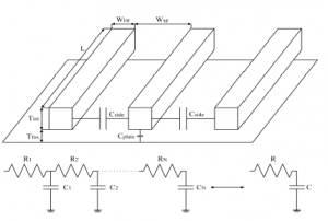
Figure 13: Variables definition used to compute the wire capacitance
This work is performed based on the CMOS 180nm process which has six metal layers. The following table provides the values of all variables defined in the formulas above.
Table 9: Values Of Variables For Wire Capacitance Calculation
Metal Layer WINT WSP TINT TFOX Cside Cplate (µm) (µm) (µm) (µm) ( µfFm) ( µfFm)
| M1 | 0.23 | 0.23 | 0.53 | 0.003981 | 0.019 | 1.456 |
| M2 | 0.28 | 0.28 | 0.53 | 0.003981 | 0.015 | 1.737 |
| M3 | 0.28 | 0.28 | 0.53 | 0.003981 | 0.015 | 1.737 |
| M4 | 0.28 | 0.28 | 0.53 | 0.003981 | 0.015 | 1.737 |
| M5 | 0.28 | 0.28 | 0.53 | 0.003981 | 0.015 | 1.737 |
| M6 | 1.50 | 1.50 | 2.34 | 0.003981 | 0.007 | 8.665 |
The table below shows the results of wire capacitance and resistance with the unit length of 1µm. In addition, the delay of each metal layer is computed by the following formula:
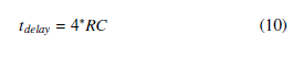
Table 10: Values Of Wire Capacitance, Resistance, Delay
| Metal Layer | Length | Capacitance | Resistance | Delay |
| (µm) | (fF) | (ohms) | (ps) | |
| M1 | 1 | 1.484 | 0.164 | 0.097 |
| M2 | 1 | 1.759 | 0.135 | 0.095 |
| M3 | 1 | 1.759 | 0.135 | 0.095 |
| M4 | 1 | 1.759 | 0.135 | 0.095 |
| M5 | 1 | 1.759 | 0.135 | 0.095 |
| M6 | 1 | 8.675 | 0.006 | 0.020 |
Based on the results above, the resistance and capacitance of a net will be calculated as the following formulas:
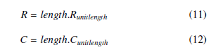
The tool in the timing analysis stage, especially the synthesis stage will calculate the capacitance and resistance of a interconnect net based on the particular length value.
5. Conclusion
In this paper, a novel approach to design a Process Design Kit (PDK) Digital for CMOS 180nm process is presented. For the Standard Cell Library design, by using the Ocean language, this work solved the problems about the licensing of the Liberty NCX tool which is unavailable in universities in developing countries, especially Vietnam, and running manually many simulations when the tool is not applied. Regarding the Wire-Load Model, this paper proposed a method and used accuracy formulas to design a complete model.
Conflict of Interest
The authors declare no conflict of interest.
Acknowledgment
This research is funded by Ho Chi Minh City University of Technology (HCMUT), VNU-HCM, under grant number BK-SDH-2021-2080912.
- C. THINH Dang, T. TOI Le, H. TRANG, “Technology Education Chal- lenges and Solution to Design a Process Design Kit for Digital CMOS
Technology in Vietnam,” in 2019 19th International Symposium on Com- munications and Information Technologies (ISCIT), 381–385, 2019, doi: 10.1109/ISCIT.2019.8905155. - X. He, X. Zhu, L. Duan, Y. Sun, C. Ma, “A 14-mW PLL-Less Receiver in 0.18- µm CMOS for Chinese Electronic Toll Collection Standard,” IEEE Trans- actions on Circuits and Systems II: Express Briefs, 61(10), 763–767, 2014, doi:10.1109/TCSII.2014.2345303.
- J. Sun, C. C. Boon, X. Zhu, X. Yi, K. Devrishi, F. Meng, “A Low- Power Low-Phase-Noise VCO With Self-Adjusted Active Resistor,” IEEE Microwave and Wireless Components Letters, 26(3), 201–203, 2016, doi: 10.1109/LMWC.2016.2521167.
- H. Liu, C. C. Boon, X. He, X. Zhu, X. Yi, L. Kong, M. C. Heimlich, “A Wide- band Analog-Controlled Variable-Gain Amplifier With dB-Linear Characteris- tic for High-Frequency Applications,” IEEE Transactions on Microwave Theory and Techniques, 64(2), 533–540, 2016, doi:10.1109/TMTT.2015.2513403.
- H. Liu, X. Zhu, C. Boon, X. He, “Cell-Based Variable-Gain Amplifiers With Accurate dB-Linear Characteristic in 0.18 µm CMOS Technology,” Solid- State Circuits, IEEE Journal of, 50, 586–596, 2015, doi:10.1109/JSSC.2014. 2368132.
- X. Tong, Y. Yang, Y. Zhong, X. Zhu, J. Lin, E. Dutkiewicz, “Design of an On-Chip Highly Sensitive Misalignment Sensor in Silicon Technology,” IEEE Sensors Journal, 17(5), 1211–1212, 2017, doi:10.1109/JSEN.2016.2638438.
- S. Chakraborty, Y. Yang, X. Zhu, O. Sevimli, Q. Xue, K. Esselle, M. Heimlich, “A Broadside-Coupled Meander-Line Resonator in 0.13- µm SiGe Technol- ogy for Millimeter-Wave Application,” IEEE Electron Device Letters, 37(3), 329–332, 2016, doi:10.1109/LED.2016.2520960.
- M. A. Capilayan, R. Minguez, J. A. Hora, “Analysis on HSpice perfor- mance trade-off versus simulation time,” in 2015 International Conference on Humanoid, Nanotechnology, Information Technology,Communication and Control, Environment and Management (HNICEM), 1–6, 2015, doi: 10.1109/HNICEM.2015.7393176.
- A. Sadhu, P. Bhattacharjee, “Methodology of Standard Cell Library Design in .LIB Format,” Journal of VLSI Design Tool & Technology, 30–38, 2014.
- J. Hu, J. Wang, “Low power design of a full adder standard cell,” in 2011 IEEE 54th International Midwest Symposium on Circuits and Systems (MWSCAS), 1–4, 2011, doi:10.1109/MWSCAS.2011.6026457.
- S. Srinivasan, M. Hogan, “Physics to Tapeout: The Challenge of Scaling Relia- bility Verification,” in 2019 IEEE International Reliability Physics Symposium (IRPS), 1–5, 2019, doi:10.1109/IRPS.2019.8720440.
- Y. Kuo, L. J. Arana, L. Seva, C. Marchese, L. Tozzi, “Educational design kit for synopsys tools with a set of characterized standard cell library,” in 2018 IEEE 9th Latin American Symposium on Circuits Systems (LASCAS), 1–4, 2018, doi:10.1109/LASCAS.2018.8399907.
- M. S. I. bin Hussin, Y. W. Lim, N. A. Kamsani, S. J. Hashim, F. Z. Rokhani, “Development of automated standard cell library characterization (ASCLIC) for nanometer system-on-chip design,” in 2017 IEEE 15th Stu- dent Conference on Research and Development (SCOReD), 93–97, 2017, doi:10.1109/SCORED.2017.8305414.
- S. Jain, M. Alioto, “A closed-form energy model for VLSI circuits under wide voltage scaling,” in 2016 IEEE International Conference on Electron- ics, Circuits and Systems (ICECS), 548–551, 2016, doi:10.1109/ICECS.2016. 7841260.
- C. K. Jha, S. N. Ved, I. Anand, J. Mekie, “Energy and Error Analysis Frame- work for Approximate Computing in Mobile Applications,” IEEE Transac- tions on Circuits and Systems II: Express Briefs, 67(2), 385–389, 2020, doi: 10.1109/TCSII.2019.2910137.
- M. Li, C.-I. Ieong, M.-K. Law, P.-I. Mak, M. Vai, R. Martins, “Sub- threshold standard cell library design for ultra-low power biomedical appli- cations,” Conference proceedings : … Annual International Conference of the IEEE Engineering in Medicine and Biology Society. IEEE Engineering in Medicine and Biology Society. Conference, 2013, 1454–1457, 2013, doi: 10.1109/EMBC.2013.6609785.
- M. U. Khan, Y. Xing, Y. Ye, W. Bogaerts, “Photonic Integrated Circuit De- sign in a Foundry+Fabless Ecosystem,” IEEE Journal of Selected Topics in Quantum Electronics, 25(5), 1–14, 2019, doi:10.1109/JSTQE.2019.2918949.
- M. Lee, S. Cho, N. Lee, J. Kim, “Design for High Reliability of CMOS IC With Tolerance on Total Ionizing Dose Effect,” IEEE Transactions on Device and Ma- terials Reliability, 20(2), 459–467, 2020, doi:10.1109/TDMR.2020.2994390.
- B. Contreras, G. Ducoudray, R. Palomera, C. Bernal, “Automated Parameter Extraction and SPICE Model Modification For Gate Enclosed MOSFETs Sim- ulation,” in 2019 16th International Conference on Synthesis, Modeling, Anal- ysis and Simulation Methods and Applications to Circuit Design (SMACD), 189–192, 2019, doi:10.1109/SMACD.2019.8795289.
- J. Bhasker, R. Chadha, Static timing analysis for nanometer designs: A practical approach, 2009, doi:10.1007/978-0-387-93820-2.
- T. J. Chang, Z. Yao, B. P. Rand, D. Wentzlaff, “Organic-Flow: An Open-Source Organic Standard Cell Library and Process Development Kit,” in 2020 De- sign, Automation Test in Europe Conference Exhibition (DATE), 49–54, 2020, doi:10.23919/DATE48585.2020.9116540.
- B. Gupta, W. R. Davis, “Characterization of Fast, Accurate Leakage Power Models for IEEE P2416,” in 20th International Symposium on Quality Elec- tronic Design (ISQED), 39–44, 2019, doi:10.1109/ISQED.2019.8697565.
- M. Olivieri, A. Mastrandrea, “Logic Drivers: A Propagation Delay Modeling Paradigm for Statistical Simulation of Standard Cell Designs,” IEEE Trans- actions on Very Large Scale Integration (VLSI) Systems, 22(6), 1429–1440, 2014, doi:10.1109/TVLSI.2013.2269838.
- K. Vaidyanathan, D. H. Morris, U. E. Avci, H. Liu, T. Karnik, H. Wang, I. A. Young, “Improving Energy Efficiency of Low-Voltage Logic by Technology- Driven Design,” IEEE Journal on Exploratory Solid-State Computational De- vices and Circuits, 4(1), 10–18, 2018, doi:10.1109/JXCDC.2018.2812242.
- N. Karagiorgos, S. Nikolaidis, “Application of the power contributors method for the AOI22 CMOS cell,” in 2019 8th International Conference on Mod- ern Circuits and Systems Technologies (MOCAST), 1–4, 2019, doi:10.1109/ MOCAST.2019.8742028.
- M. R. F. Abingosa, C. Receno, J. Imperial, J. A. Hora, “Interconnect mod- eling of global metals for 40nm node,” in 2015 International Conference on Humanoid, Nanotechnology, Information Technology,Communication and Control, Environment and Management (HNICEM), 1–6, 2015, doi: 10.1109/HNICEM.2015.7393172.
- T. Sakurai, K. Tamaru, “Simple formulas for two- and three-dimensional ca- pacitances,” IEEE Transactions on Electron Devices, 30(2), 183–185, 1983, doi:10.1109/T-ED.1983.21093.