The Probe Mark Discoloration on Bond Pad and Wafer Storage

Adv. Sci. Technol. Eng. Syst. J. 5(6), 416–422 (2020);
 DOI: 10.25046/aj050650
In this report, a probe mark discoloration with donut/circle shape was found. The corrosion formed on Aluminum bond pads. The SEM/EDS, TEM/EELS & AES surface techniques were used to identify this corrosion product. All these material analysis results pointed out the role of fluorine to this discoloration. The HAST testing, all the chip samples obtained from wafer center/middle area, were simulated to have been exposed in air for 1 year. HAST test result showed no fluorine source came from the center/middle zones of impact wafers. Another full wafer-level FOSB storage test showed the source of corrosive fluorine came from wafer itself. EDS mapping results, from extreme wafer edge zone, indicated the fluorine element distribution. The mechanism of this novel discoloration was proposed. However, more evidences were necessary for understanding the formation of donut discoloration corrosion.
1. Introduction
In order to obtain semiconductor device electrical performance, the circuit probing (CP) tests were performed by pin probing on bond pad before device package process. The typical bond pad materials are Aluminum (Al) with low content of silicon and copper to improve the resistance of electron migration. The interconnection from aluminum pad surface to external interface frame play a critical role in semiconductor package process. It is well known the Aluminum would form corrosion protective oxide film in oxygen condition. However, in the past three decades, the formation of fluorine (F) corrosive film on aluminum bond pad surface [1,2] and non-stick on pad (NSOP) failure issue that induced broad quality issues concern were reported by some researchers before. [3-7] These corrosive film was found to suffer semiconductor reliability. The early researches indicated two main root causes for these fluorine contained contamination. One is the fluorinated silicone glass (FSG) film could release fluorine into closed spacing, and then contaminate the bond pad surface. [1] The FSG layer is still an important low K dielectric layer used in device process, so the F leakage from FSG layer is still a unavoidable issue in semiconductor dielectric layer process. The second fluorine source is the fluorine embedded on Al pad surface, and the fluorine residue from previous pad etching and cleaning gas. [9] So the fluorine source for contamination divided into two groups, direct F embedded on Al top surface, and the indirect F from FSG layer. Therefore, the wafer storage become an important factor for fluorine contamination. The early F-induced contamination studies focused on the morphology and mechanism to induce corrosion product. No probe mark and electric testing effects were reported before. P. Chang [8] had stated the early probe mark discoloration study of yellow discoloration Al bond pad corrosion. However, the probe mark discoloration had not been fully report yet. [10, 11] In this paper, the donut/circle discoloration corrosion and a compressive study would be present.
In the beginning of this case, the probe mark discoloration was found at the stage of blue tape. All the impacted wafers finished all the CP tests, and stored in the Front Opening Shipping Box (FOSB) for more than two months. There are two types of probe mark discoloration forming on the bonding pad surface. Figure 1 (a) and (c) show these typical circle/donut discoloration optical microscope (OM) photos. The special feature of discoloration morphology is that probe mark is the center of cyclic/donut center. The OM inspection for discoloration corrosion indicated most of the corrosion was cyclic, and only few was donut shaped. Figure 1 (b) show that two touchdown would not induce two discoloration. The size of cyclic discoloration is not constant, however, the largest diameter of a suffered wafer, up to 35 um, is nearly the same. With the help of full wafer dice Auto Vision Inspection (AVI), most of the corrosive dice locate near the wafer edge zone. The worst fail rate would reach up to 15-18% of all the available dice.
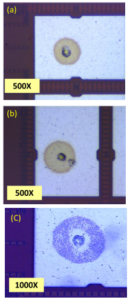
Figure 1: (a) show the typical probe mark discoloration OM image. (b) show the formation of discoloration on Al pad under dual pin touch down. No second discoloration is found. (c) show donut-shaped probe mark discoloration. To clearly show donut shape discoloration, (c) was magnified to 1000X, that is larger than Figure 1 (a) & (b).
2. Experiments and Results
In this study, the samples were checked in plane-view & cross-sectional approaches. The Scanning Electron Microscopy (SEM) images was obtained by 5 KeV electron energy. And the Energy Dispersive Spectrum (EDS) result was obtained by 10 KeV electron energy. Transmission Electron Microscopy (TEM) operated at 200 KeV with Electron Energy Loss Spectrum (EELS). SEM and TEM could get the information of morphology and corresponding EELS analysis for the normal and abnormal locations. Auger Electron Spectroscopy (AES) is a traditional surface analysis technology for bond pad corrosion case. So AES depth profile results would be included.
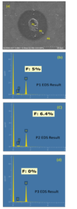
Figure 2: (a) is the SEM micrograph of probe mark discoloration corrosion. P1 is the zone of probe mark. P2 is the discoloration zone. P3 is the normal Al pad surface. (b),(c) & (d) the corresponding EDS analysis result of P1 to P3 various zones on Al pad surface. The oxygen element was found for each locations. The Fluorine was only found at the discoloration zones.
Based on the literature review, the various storage conditions would impact corrosion behavior. Highly Accelerated Stress Test (HAST) was applied with test conditions of temperature at 130ºC and RH 85% for 21 hours. This test is to simulate all the bond pad exposed in air without Nitrogen Cabinet storage or Moisture Barrier Bag (MBB) storage for 1 year. This test would be helpful to evaluate the impacted dies corrosion behavior. The secondary storage test, full wafer deposited in the regular FOSB, is to identify the standard FOSB storage effect, and find out the source of F element.
2.1. SEM/EDS Analysis Results
Figure 2 show the top-view SEM photo and corresponding EDS analysis results of various feature locations on Al pad surface. The SEM photo clearly show the boundary of discoloration boundary on Al pad surface. Based on the SEM inspection, the rough size of this discoloration was more than 25 micro meter. The probe mark and corresponding discoloration zone were easily identified. The SEM photo also show various morphology of probe mark surface deformation. According to the EDS results of discoloration zone, the P1 & P2 of Fig. 2(a), where fluorine and oxygen contents are found on the center and middle of circle region. No Fluorine element was detected for normal P3 Al pad surface. The content of fluorine element, 5-6 %, is noted. That is, the probe mark discoloration is a kind of aluminum-fluorine-oxygen corrosion. As for the normal zone, aluminum oxide form on Al pad surface. Since this novel corrosion product has not been fully reported before, the EDS analysis is helpful to improve the key role of fluorine element.
Figure 3 show the OM photo and its corresponding EDS result. P1 to P4 of Figure 3(a) are the various locations of donut-shaped discoloration on Al pad surface. P1 is the probe mark zone. P2 is the cyclic annular zone without discoloration. P3 is the cyclic annular zone with discoloration corrosion. And P4 is the normal Al pad surface. The EDS result clearly indicate fluorine element is only found at the discoloration corrosive zone. No fluorine is found at P1- probe mark, P2- cyclic annular without discoloration, and P4 – normal Al pad surface zones. Based on these donut-shaped discoloration EDS results, the root cause of the discoloration event is due to fluorine contamination. However, due to the basic characteristic of high energy electron stopping power, the X-ray signal of EDS analysis is collected not only from Al pad top surface, but also the larger undersurface bulk volume. The distribution of fluorine element could not be identified by this EDS analysis. TEM and AES are necessary for further identification.
2.2. TEM/EELS Analysis Results
The cross-sectional TEM inspection is helpful to identify the thickness variation of corrosion film. Figure 4 show the full cross sectional TEM inspection photo of discoloration area. The thickness of discoloration corrosion film is just a few nm. Therefore, it could not be clearly identified by Figure 4. The magnified TEM photo indicate the thickness of discoloration film is uniform except for probing mark zone. Figure 5 show the High Angle Annular Dark Field (HAADF) TEM image of discoloration film structure. The HAADF image indicate the thickness of circle shape discoloration is within 5 nm. The corresponding Electron Energy Loss Spectrum (EELS) line scan results show the F & O distribution of this Al-O-F film. The fluorine is found on the top surface of corrosion film. No F & O could deeply penetrate into the Al. Figure 4 show the corrosion film of probe mark is complex. Figure 6 show the high magnification cross-sectional TEM image and its corresponding EELS data of probe mark oxidation. The variation of corrosion film thickness might be up to over 10X. The thicker film formed on probe mark zone is also the AL-O-F compound as other discoloration zone. The EELS fine structure analysis indicate discolored Al2O3 spectrum is a combination of
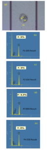
Figure 3: (a) is the OM image of donut-shaped probe mark discoloration. P1 is the zone of probe mark. P2 is the annular zone without discoloration. P3 is the annular zone with discoloration. P4 is the normal Al pad surface. (b), (c), (d) & (e) the corresponding EDS analysis results of various zones on bond pad surface. Fluorine is only found at the cyclic annular discoloration zone.
pure Al2O3 with OF3. That is, the fluorine diffuse into the Aluminum oxide film. F atom form a new bonding to replace O bonding. These new formed Al-O-F must be less protective than original Al2O3 film.
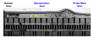
Figure 4: The low magnification full cross-sectional TEM image of discoloration defect corrosion.
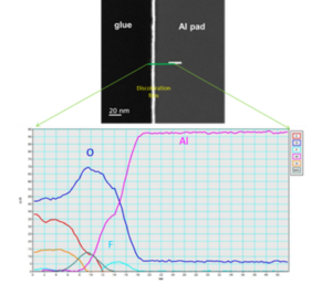
Figure 5: The cross sectional HAADF TEM image of discoloration zone and its corresponding EELS line scan result. The line scan result clearly show the distribution of fluorine and Oxygen just on the Al pad top surface.
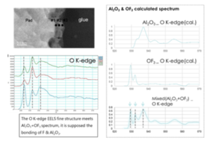
Figure 6: The TEM image and EELS data of probe mark discoloration defect film & its corresponding simulation EELS spectrum.
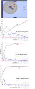
Figure 7: The OM photo and the corresponding AES depth profile of P1, P2 & P3, the P1, P2, & P3 are marked on discolored Al pad surface. P1 is the probe mark zone. P2 is the discoloration zone. P3 is the normal Al pad surface. The F element is found to co-exist with Al2O3 at discoloration zones.
2.3. AES Analysis Results
For a long time, the AES analysis is treated as the standard technology for Al pad surface contamination. Figure 7 (b) to (d) show the specific Auger Electron Spectrum (AES) depth profile result of normal/discoloration area of bond pad surface. The AES result indicate the main elements of probe mark and cyclic discoloration area are Al, F, and O. That is the same as previous EDS & EELS results. The AES depth profile results, P1, P2 & P3 of Figure 7, show the discoloration corrosion film is the F element co-existed with AlxOy. BTW, X-ray Photon Spectrum ( XPS ) is also an available surface analysis technology for oxidation state of Al compound. However, due to the X-ray focusing capability limitation, XPS is not used in this bond pad case. The Secondary Ion Mass Spectrum (SIMS) analysis meet the similar limitation.
Two key factors decide the success of this contamination Failure Analysis. The first one is to identify the component of the corrosion product. The second one, sometimes it is more critical in probe testing FAB daily operation, is to find out the corrosion/contamination source, and then to stop this event.
Based on previous material analysis finding, the probe mark discoloration contamination is a special type of Al-F-O corrosion. Since the nature protective Al-O film would automatically form on bond pad top, therefore, the fluorine element play an important role in this corrosion event. Where do the fluorine come from? How do this discoloration develop?
The fluorine induced corrosion on Al bond pad is not an new issue[1,2]. The source of fluorine might come from wafer itself or external environment. The fluorine come from wafer itself is supposed to be the etching residue on Al pad surface.[9] The F-contained etching gas, like CF4, is broadly used in Al pad process loop. The fluorine element is supposed to easily residue on Al pad top surface after etching. Generally speaking, the 5 % fluorine residue on Al pad surface is regarded as a safe margin. However, the previous AES depth profile data indicate no fluorine element is found below 1.5nm of top surface on no discoloration area of Al pad. The source of fluorine need to clarify. Therefore, two various storage tests are necessary to find out the fluorine source. The first storage tests, HAST, the dice-level test is a high temperature corrosion accelerated test. The second test, FOSB storage test, is a full wafer-level test under daily standard storage operation. The experiment results show as below:
2.4. HAST Storage Test Result
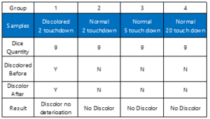
In order to clarify the effects of long time storage and probing touchdown number on this corrosion. Four groups of various die samples were applied for the HAST. The nine discolored and nine normal dice were the first and secondary groups for HAST. The nine dice, with five and twenty probing touchdowns, set as the third and the forth groups. Therefore, in this HAST, total four groups dice obtained from impacted wafers were tested. The HAST testing preformed at the condition of temperature 130ºC and RH 85% for 21 hours. All the dice samples simulated to have exposed in air without N2 cabinet storage or MBB bag storage for 1 year. Table 1 consolidate the result of HAST storage test. The result of group one and two indicate that there is no visual change, by 100% OM inspection, after HAST storage simulation testing. No probe mark discoloration corrosion size increase after HAST. The secondary group data indicate no probe mark discoloration would form. The result of third and four group imply that the heavy deformation on Al pad surface would not automatic induce discoloration corrosion. According to the previous analysis, the fluorine is necessary for the formation of discoloration. The HAST result show no extra fluorine source exist in HAST tested dice.
Table 1: The HAST testing Result. Four various samples were tested. The size of all samples are die level. The discoloration dice show no deterioration after the test. No other tested dice show clear change. In this table, Y means discoloration; and N means no discoloration.
2.5. FOSB Storage Test Result
Based on the previous HAST result, all these dice were obtained from wafer center or middle area, and no extra fluorine was found. The FOSB storage test preformed for the full wafers deposited in normal FOSB at room temperature. The Ardentec AVI inspection was applied for the tested wafer before FOSB storage testing. Then these wafers, after some storage time, would be viewed by Ardentec standard AVI checking to identify the discoloration behavior on the same Al pad. After 4 weeks’ storage time, obvious variation was found. Figure 8 clearly indicate the variation of two OM photos. The probe mark discoloration would deteriorate in FOSB storage test. That is to say, the fluorine-induced corrosion in the FOSB volume would be continuous. It is a manifest evidence the source of F element enhancing discoloration corrosion is due to the full wafers FOSB storage. The HAST result indicated no extra F was found from wafer center and middle area. Therefore, the source of F element of FOSB test is highly suspected to be the wafer edge or wafer extreme edge area. The EDS mapping was an excellent technology to show the various element distribution of semiconductor top surface. It would be helpful to identify the distribution of fluorine element of abnormal wafer extreme edge area.
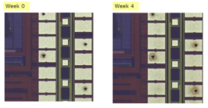
Figure 8: show the OM inspection result after FOSB storage test. The original probe mark discoloration is the OM micrograph on the left. After 4 week’s FOSB storage, the size of probe mark discoloration became larger. The right hand side OM photo clearly show this deterioration.
Figure 9 show the EDS mapping result of extreme edge area of discoloration wafer. The EDS data clearly show the distribution of F, Al and other main elements on semiconductor wafer top surface. And the original location of this EDS mapping, the right hand side OM photo of Figure 9, was obtained at the extreme edge of full wafers. There is a clear boundary between extreme edge, the upper part of OM image, and the internal die area. The fluorine-induced corrosion source is clearly identified from extreme edge of full wafers. It is supposed that the FSG layers exposed to FOSB space would be the F source of this corrosion.
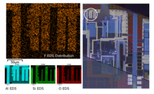
Figure 9: The EDS mapping result of Al pad on the discoloration wafer extreme edge area. The left hand side EDS mapping result show the distribution of F, Al, Si and O. The white circle area of right-hand side OM image shows the location of this EDS area of the wafer.
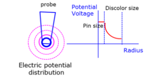
Figure 10: The critical CP testing and electrical testing potential field effect on Al bond pad surface.
The mechanism of this probe mark discoloration was proposed as follow: The CP testing would activate the embed fluorine. The formation of fluorine-contained oxide film induce this special discoloration.
The special point of this novel discoloration is the corrosion morphology with probe mark as its center. Some factors inducing the fluorine activation would spontaneously lead the probe mark as the discoloration cyclic center. In the beginning, the CP probing action would induce a permanent mechanical damage on the Al bond pad surface. This damage produce great deformation and heavy strain on the Al pad top surface, and this deformation and strain region, chemical activated, would be full of dislocation-like defects. The second mechanical effect was that probing test itself would break down the original protective Al-O film, and then create large amount of fresh aluminum surface. Both the mechanical effects would induce extremely active sites on Al pad surface. These would be easily for fluorine to react with Aluminum. The other impact of the probing action is the corresponding electric field potential, built by Circuit Probing test, would have an effect on the surrounding area of probe mark under the voltage/current variations. Under certain temperature, like the temperature of 125ºC setting at CP testing, and humidity, the fluorine contamination would be excited. Here the water is supposed to play an important role, leading to forming of hydrogen and oxygen, and after serial chemical reaction with fluorine, the AlxOyFz compound form. This kind of AlxOyFz compound is the discoloration by OM inspection. The threshold activation energy for all the chemical reactions was limited by electric potential field built by testing program, therefore, electric potential field introduced the circle shape discoloration region centered by probe mark. Figure 10 show the electric potential field distribution build by probing test.
The formation of probe mark discoloration on Al pad surface was not just due to single factor. There are three complex factors to induce this corrosion. The first factor is the sufficient fluorine supply in wafer storage environment. The fluorine might come from bond pad top surface or wafer inter metal dielectric layer. The second one is the environmental condition. The suitable temperature and enough humidity are critical to accelerate the fluorine corrosion reaction. The third factor induce probe mark discoloration formation was the probing touchdown and its sequential current and electric field. According the early study [3], the Al-O-F compound on Al pad surface show different morphology as this corrosion event. No previous report had pointed this Al-O-F compound discoloration morphology with probe mark as its circle center. Therefore, the characteristic of this contamination closely related to electric probing test condition. Then this novel probe marked discoloration need to combine all the above corresponding factors. These factors are materials property, wafer testing/storage environments and probing testing. Figure 11 show this idea.
According to the above mechanism, the formation of probe mark discoloration could stop in some ways. The material itself decide the source of fluorine. Therefore, the content of fluorine embedded on bond pad top surface or the distribution of fluorine on wafer edge is an important index to find the fluorine source. Since in CP and FT daily operation, no fluorine contained chemical materials are used. The CP & FT Fab is better to take them into regular monitor index for future discoloration event.
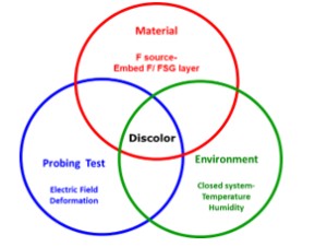
Figure 11: The factors to induce bond pad probe mark discoloration. These critical factors are material property, probing test and environment.
In the previous discoloration mechanism, the formation of donut shaped discoloration corrosion would be a weak point. Since the material analysis of donut discoloration indicate the fluorine contained discoloration would only form on the ring zone, and no other discoloration would form on the other Aluminum pad surface. Therefore, the idea, discoloration originally form at probe mark area, and then fluorine diffusion to deteriorate discoloration, would not fully explain the formation of donut-shaped discoloration corrosion film. The EDS analysis result of donut-shaped discoloration imply that no fluorine exist at probe mark area. This impressive result also indicate the probe mark area with heavily deformation and high dislocation density would not spontaneously form corrosive fluorine contained Al-O-F film. The limitation of fluorine supply might be the key factor for this donut-shaped discoloration. There is no enough fluorine to form Al-O-F film on probe mark area, but enough fluorine to form Al-O-F film on annular area of Al top surface. In this system, there are two fluorine source, the embed fluorine and leakage form FSG. It is supposed that the embed fluorine would spontaneously form Al-O-F during CP testing under suitable electric potential activation. The fluorine supply from FSG leakage would be slowly deteriorate the corrosion due to diffusion into spacing is a time consuming process. That is to say, discoloration might be separate into two stages. In the first stage, embed fluorine play the key role in Al-O-F corrosion film formation. As for the secondary stage, the fluorine accumulation, leakage from FSG, and diffusion to Al-O-F interface play the key role. The secondary stage is a time consuming stage, therefore, storage environment is the controlled factor at this stage. The formation of cyclic discoloration corrosion would be that there is enough embed fluorine on the Al bond pad surface, and following with enough fluorine from FSG layer. As for the donut shaped discoloration, it would be that no enough embed fluorine on bond pad surface, so there is no complete cyclic discoloration formation. The key factor for donut-shaped discoloration formation is the supply of fluorine. No fluorine to react with Al metal. This explain that no Al-O-F film form at probe mark area and the formation of annular corrosion film. The possible root cause for donut discoloration might due to fluorine source complete consumption. However, no experiment would prove this proposal now.
3. Conclusions
- A new donut/circle shaped discoloration on Al bond pad is reported.
- Based on SEM/EDS, TEM/EELS and AES analysis results, the novel discoloration is due to form an Aluminum fluorine-oxide compound. The fluorine plays a key role in the formation of probe mark discoloration.
- With the help of HAST, FOSB storage test, and EDS mapping, the source of fluorine of this case is found.
- Since probe mark is the center of circle for discoloration, the formation of this corrosion is closely relative with the CP electric field.
Conflict of Interest
The authors declare no conflict of interest for this work. Formal “Conflict of Interest” document file is attached.
Acknowledgment
The authors would like to thank Polly Liu and Alex Si for their long time effort on discoloration impacted wafer management, and Berton Hsieh and Wei-Cheng Chen for their long time supporting on FA analysis.
- K. Ernst, D. Grman, R. Hauert, E. Holländer “Fluorine-induced corrosion of Aluminum microchip bond pads”, Surface and Interface Analysis, 21(10), 691 – 696, 2004, doi: 10.1002/sia.740211003
- W. A. P. Claassen and P. Krarner, “Aluminum Corrosion in the IC-MOS Production Line”, Internal Report. Philips, Nijmegen, 1988.
- Hua Younan, Shailesh Redkar, Lau Chi-Kwan and Mo Zhiqiang, “ A Study on Non-Stick Aluminum Bond Pads due to Fluorine Contamination using SEM, EDS, TEM, IC, Auger, XPS & TOP-SIMS Techniques”. in The Proceeding from the 28th International Symposium for Testing & Failure Analysis (ISTFA 2002), Phoenix, USA, pp. 495-504, 2002.
- H. Younan, Shailesh Redkar, Ron Dickinson, and Peh Shirley, “A study on Fluorine-Induced Corrosion on Microchip Aluminum Bond Pads”. in The Proceeding from the 29th International Symposium for Testing & Failure Analysis (ISTFA 2003), Phoenix USA, pp. 249-255, 2003, doi: 10.1002/ sia.740211003
- Karl-Heinz Ernst, R. Hauert, E. Holländer, “The Fluorine-induced corrosion of Aluminum microchip bond pads”, Surface and Interface analysis, vol.21, 691-696, 1994, doi: 10.1002/sia.740211003
- Sethu, R. S., “Reducing non-stick on pad for wire bond: A review” Australian Journal of Mechanical Engineering, 9(2), 147-160, 2012, doi: 10.7158/M11-771.2012.9.2
- H. Younan, Nistala Ramesh Rao and Teong Jennifer, “Studies of Fluorine-induced Corrosion and Defects on Microchip Al Bond pads and Elimination Solutions” in The Proceedings from the 34th International Symposium for Testing and Failure Analysis, Portland USA, pp. 285-290, 2008, doi: 10.1361/cp2008istfa285
- P.Chang, H.L Hsiao, C.H Cheng, S.I.Chu, H.W.Tai, Y.Y Shieh, C.Y Sun, “Investigation of Fluorine Induced Probe Marker Discoloration,” in 2013 IEEE 15th Electronics Packaging Technology Conference (EPTC 2013), Singapore, pp. 139-142, 2013, doi: 10.1109/EPTC.2013.6745700
- J.H. Linn, W. E. Swartz Jr., “An XPS study of the plasma etching of aluminum with CCl4”, Spectroscopy Letters, 18(5), 335-352, 1985, dio: 10.1080/00387018508062236
- W.F. Hsieh, Henry Lin, Vincent Chen, Irene Ou and Y.S. Lou, “The Investigation of Fluorine Induced Novel Probe Marker Discoloration”, in The Proceeding from the 44th International Symposium for Testing & Failure Analysis (ISTFA 2018), Phoenix USA, pp. 413-417, 2018.
- W. F. Hsieh, H. Lin, V. Chen, I. Ou and Y. S. Lou, “The probe marker discoloration on Al pad and wafer storage,” 2019 IEEE 26th International Symposium on Physical and Failure Analysis of Integrated Circuits (IPFA), Hangzhou, China, pp. 1-4, 2019, doi: 10.1109/IPFA47161.2019.8984909.
No related articles were found.