DC-DC Buck Converter Driver with Variable Off-Time Peak Current Mode Control

Adv. Sci. Technol. Eng. Syst. J. 5(6), 347–352 (2020);
 DOI: 10.25046/aj050642
Power converters in automotive industries are needed to source electronic devices. DC-DC Buck converter allows to drive loads ensuring their safety operation taking the car battery voltage as an input to generate a sub-voltage or current. By means of a control loop, the system makes sure that the output variable has the desired value in each operation condition. The Peak Current Mode Control (PCMC) is used to control the output current. Whenever the current reaches the reference maximum value (by load specs), the system acts to lower it. Intrinsically over-current protection is guaranteed. The paper presents an improvement of the basic PCMC, where, instead of just controlling the peak value, the loop controls also the average, more delicate feature, resulting in a more reliable driver system. The circuit is able to source 3A average-4.5V from a 13.5V nominal battery voltage, with a peak current of 3.3A and a 0.6A maximum ripple (3 10%A). The concept has been designed and simulated on Simulink and then tested on hardware using dSpace, a Rapid Control Prototyping set-up.
1. Introduction
(CCM). Instead of having a constant switching period, as it happens in the typical PCMC, the presented control loop has a variable period. In particular, the time in which the power-DMOS stays off, Electronic devices in Automotive industries need for power conchanges accordingly to the calculated current average value, to make verters to be correctly sourced. Indeed, battery voltage could range between 4.5 to > 27V, making it unsuitable for driving any load it closer to a target desired value. The loop will be now on referred without provoking damages or malfunctions. DC-DC Converters al- to it as Variable Tof f . Moreover, the typical PCMC intrinsically suffers of instability issues directly attributable to the fixed switching low to take as an input the car battery voltage and return as an output frequency [4]. Therefore, by making it variable, such issues are cona controlled voltage or current required by the load. What is more, sequently solved. The use of stabilization techniques such as Slope the DC-DC protects the load against over-current and over-voltage,
Compensation [4] can be avoided, which increase the complexity ensuring its correct operation. Meanwhile, integrated circuits are of the system without improving the control precision (indeed currequired to occupy small space and reduce external components to rent features will change accordingly to the input voltage). Also minimize the associated cost. The core of a Buck DC-DC converter protection against over-current is already guaranteed: indeed the is a switch, or Power-DMOS, which is repeatedly turned on and maximum current, namely the peak, is fixed. The proposed system off, allowing the voltage/current to increase/decrease quickly in the operates with 500kHz maximum switching frequency, delivering an neighborhood of a desired value. The circuit that turns on and off average output current of 3 ± 10%A with a load-fixed 4.5V output the switch is the control circuit [1]. The control could be either voltage. The current peak will be limited to 3.3A. The application made on the output current or voltage. This paper presents a current case could be, for instance, a LED driver, where the LED itself, as control loop able to control all the current features (peak, average soon as the correct current is provided, fixes the output voltage. The and ripple) at once. This paper is an extension of work originally circuit has been simulated and then tested in laboratory by using an presented in the 26th IEEE International Conference on Electronics emulator called dSpace. Instead of a LED, in first place has been Circuits and Systems (ICECS) [2]. used as a load a linear component: a 1.5 Ω resistor. The solution arises from the well-known Peak-Current-Mode an external pad to sense the current, resulting in a lighter circuit. Compared to the most common solutions [5], the here used fullyintegrated Current Sensing technique requires less external components, with consequent lower cost in terms of BoM and board fabrication.
The paper is organized as follows. The algorithm principle is presented in Section II, together with the formula useful for its implementation, described in Section III. The simulation results are shown in Section IV and the conclusions are drawn in Section V.
2. Variable-Tof f PCMC Algorithm
A Buck DC-DC converter is a device which in principle allows to convert a given input voltage to a lower output voltage by turning on and off a Power-DMOS, able to withstand to high power. In the application at stake from [4.5,27]V are obtained 4.5V in output by controlling the current, IL, flowing into the load. A simple scheme of a Buck converter is given in Figure 1.
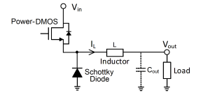 Figure 1: Buck converter scheme
Rather than other diodes, a Schottky diode has been used for its lower threshold (0.5V) and higher speed. The presence of the output capacitor, which minimizes the voltage ripple, can be neglected when controlling the current (and the output voltage is fixed by the load) leading to a lighter circuit. The switching period is divided into two phases: the ON-phase when the Power-DMOS conducts (Ton) and the OFF-phase when the diode conducts (Tof f ). Referring to the Duty-Cycle (D):
The Buck converter should sink an optimum average current
Iavg to make the load work properly and, to avoid damages, the current must fluctuate limitedly. The current ripple should be indeed limited to the average value±10%, namely 0.3A. Consequently, the maximum current, the peak value, should be 3.15A. The rule of the control loop is to ensure that these specifications are met. The relation between the current features can be expressed as follows:
![]()
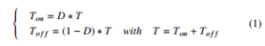
In standard PCMC, the period T is fixed. Conversely, in Variable Tof f , the period is variable. In particular, Ton changes automatically according to the input voltage, while Tof f is forced to vary every cycle by the control loop, based on the vicinity between the calculated output average value of that cycle and the desired value.
The load current during the ON-phase increases with positive slope given by:
![]()
Once IL reaches Imax, the power-DMOS turns OFF and the output current decreases with a negative slope:
![]()
After a time Tof f , the DMOS is turned ON again and so on. The output current waveform (equal to the inductor current) has the typical triangular CCM shape as in Figure 2.
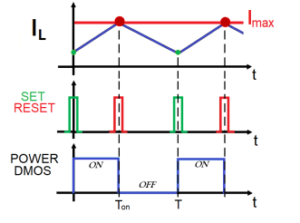
Figure 2: Output current
While Imax is fixed, the Imin is free to change. The loop, by means of a sensing technique, is able to read Imin. Indeed, the current sensing happens during the ON phase to insure the current doesn’t grow beyond Imax. Therefore, to get Imin, it just needed a register to store the first current value when the ON phase begins.
Once Imin is known, the loop calculates:
![]()
Then, the difference between Iavg and Imean,ref = 3A gives an error with sign that, once properly amplified by a factor K, is summed to the previous Tof f value. The following Tof f value will be:
![]()
In this way, if e.g. Iavg is higher than 3A, the Tof f value will be increased (causing a stretching of the switching period) and allowing the current to decrease more during the OFF phase, reaching a lower Imin with the aim of reducing the average value. If otherwise
Iavg is lower than 3A, the error will be negative, meaning that the
Tof f of the next switching cycle must decrease to make the average value higher and matching with the target. The loop operation is resumed in the flow-chart in Figure 3. The total number of regressions in the algorithm depends on the current rising slope, on the sensing technique sampling frequency and on the counter frequency. Every time a switching cycle ends, the operation restarts from the beginning giving rise to the next switching cycle.
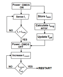
Figure 3: Variable-Tof f PCMC algorithm flowchart
While Tof f is decided by the loop, the Ton, from (3), changes not only with the the ∆IL -loop dependent- but also with the battery voltage:
![]()
It should be noticed that a first pre-memorized Tof f value guess must exist (to be later overwritten by the cycle) to avoid malfunction at the cranking of the system during the very first switching cycle. This first guess is based on the application: if for instance the desired average is 3A, the peak is 3.15A, the inductance 30µH and Vout = 4.5V, it follows that the Tof f value, from (2) and (4), could be grossly chosen as:
![]()
Then, given some Vout variations due to the load or some uncertainties related to the inductance value, the references etc., the loop will act as described above, varying the Tof f value to better adapt the system to the load specifications.
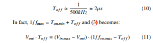
Moreover, the Tof f value has an inferior limit, due to the maximum power-DMOS frequency (fmax) allowed. Ideally, the fmax can be evaluated for Ton tending to zero, namely:
![]()
In realty, the minimum Ton value won’t be zero, but, from (3), for a Vin = 27V it will be about 0.8µ s.
3. Instability digression
The typical PCMC loop is just able to control the maximum load current, no matter what ripple and average current are. Therefore, such a solution is not suitable in applications where loads require a precise average current with small shifts around its value. However, the biggest issue of the typical PCMC comes from its instability when the duty cycle grows over 50% [6]. Every time Ton > Tof f or, equivalently, Vout > Vin/2, the system would be unstable. In the application case, where Vin = [4.5,27] V and Vout = 4.5 V, problems would arise when Vin < 9V. Figure 4 shows what happen when crossing the limit case D = 0.5: if the duty cycle is increased the PCMC is no longer helping in controlling the current. The reason behind this issue is that, in typical PCMC, after a fixed period T, the power-DMOS is forced to be turned ON. Instead, in Variable-
Tof f , the power-DMOS turns ON Tof f seconds after the current has peaked. Contrarily to the typical PCMC, if the input voltage changes, i.e. Ton changes, the Tof f doesn’t change (4), the ripple doesn’t change and therefore the current features are not impacted. The system stays stable. Techniques as Slope compensation [4] are no longer needed.
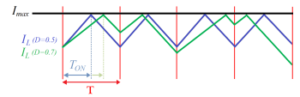
Figure 4: Output current in typical PCMC
4. Constant-Tof f Algorithm Implementation
The circuit implementation is shown in Figure 5. The only external components are the inductor (L) and the Schottky Diode. As internal components, enclosed in blocks, there are: the Current Sensing, the Control Logic blocks, the Protection, the Internal Reference (including a bandgap voltage reference to generate Imax and Imean), the Gate Driver to turn ON and OFF the Power-DMOS [7] and the Power Supply to generate a low voltage domain for the low-side circuit.
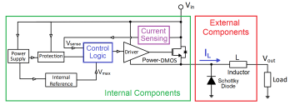
Figure 5: Concept top level
The Current Sensing block is used to read the current flowing IL. The Power-DMOS current is here mirrored with a factor N = 1/1000 and flows through a sensing resistance. Based on the read voltage drop, the system is able to determine the magnitude of the current. Since the proposed technique only operates during the ON-phase (when the Power-DMOS conducts) the power consumption is lower than in the case on which the current is sensed on the output node, always operating. Furthermore, an internal sensing block also allows to minimize the area occupation on silicon.
4.1. Control Logic block
Figure 6 shows the concept Control Logic block implementation. The result of the comparison between Isense and Imax gives the Reset of the SR Latch. When Isense ≥ Imax, the Reset activates and the Power-DMOS turns OFF through the Gate Driver. The Set input is instead connected to a counter consisting of an oscillator and a chain of four D Flip-Flops. As soon as the Power-DMOS turns OFF, the counter starts counting up to Tof f duration. Afterwards the Set is activated and the Power-DMOS turns ON. The current value at this moment, Imin, is stored into a register. The loop then calculates the average error on respect to the desired Imean value. The error, summed to the previous Tof f,prev value returns the Tof f,next as in (6).
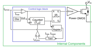
Figure 6: Variable Tof f Current Control Loop implementation
5. Design example and Simulations results
Table 1 resumes the application specs.
Table 1: Summary of specifications
| Technology | 0.35 µm |
| Vin | 4.5-27 V |
| Vout | 4.5 V |
| fmax | 500 kHz |
| Maximum Current Level | 3.3 A |
| Mean Current Level | 3 A |
| Output Current Ripple | 0.60 A |
By applying the formulas given in Section I, the design parameters are obtained. (9) gives the lower Tof f limit:
Therefore a more precise estimation of the minimum Tof f value is given by:
![]()
Once the ripple (Table 1) and Tof f (12) are given, both the peak and the average current are fixed. Furthermore, by using these parameters in (4), the inductance value can be chosen as:
![]()
(to stay large, considering also 20% of inductance value uncertainty on the nominal value and considering that actually the typical operation is centered around Vin = 16V).
5.1. Simulation results
The concept of Figure 5 has been firstly implemented on Simulink (MATLAB) to ideally simulate the behaviour of the high-level concept design. Simulink works with a block approach system, shown in Figure 7, which follows exactly from Figure 5. Other software are actually exploited in the design phase (such as Virtuoso-cadence). However, there, the circuit must be designed in a deeper transistorlevel. Since the design may take large amounts of time, prototyping must be done previously ensuring that the chosen topology is the most suitable one for the application in question and that its worthwhile to proceed with transistor-level design and future fabrication.
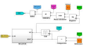
Figure 7: Simulink implementation
The simulations include also worst case scenarios to ensure the correct operation in each condition. To simulate the presence of a load which fixes the 4.5V output voltage with a 3A average current, a 1.5Ω resistor has been used.
Figure 8 (left) shows how the system works with a 7V input voltage and a peak reference reduced from 3.3A to 3.2A, i.e. with a ∆IL = 0.4A. As expected, the operation is not affected by instability issues which, in a typical PCMC, would surely arise whenever
Vin < 9V. Later, the input voltage has been abruptly increased to
18V to also prove that a Vin change (as could happen during the cranking of the car) has no relevant effect on the operation. The Tof f remains unchanged (no dependency on the Vin) and equal to 2.7µs as expected from (7) (with ∆IL = 0.4A).
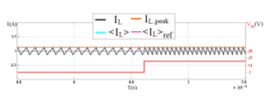
Figure 8: System response changing the input voltage
Figure 9 shows instead the transient simulation plot for Vin =
18V with the peak reference at 3.3A as from specification. As expected from (7), the Tof f = 4µs. To further prove the system robustness, an average reference positive step (from 3A to 3.15A) has been added. In order to achieve the new average current, the loop gradually reduces the Tof f to make the calculated average equal to the target. Since the peak reference stays equal, according to (8) and (9), the ripple reduces and the switching frequency increases up to 260kHz.
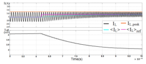
Figure 9: System response changing the average reference

Figure 10: Buck Converter and Gate Driver PCBs
Once proven the concept works as expected, the system can be tested in laboratory by means of a rapid control prototyping called dSpace. Here, the power-DMOS and external components are no longer digital, but located on a DC-DC converter Printed Circuit Board (PCB), which is connected to a Gate driver board (Figure 10), connected in turn to dSpace.
dSpace, through its FPGA, will embody the Simulink bloch approach control logic circuit (uploaded by PC), also providing the current sensing, the internal reference and all the devices to communicate with the hardware (ADCs, DACs). dSpace allows to test whatever control circuit including all the un-idealities of the system, verifying moreover the correct operation of the power-DMOS and that one of a real load. In this way it can be eventully proven that, not only the circuit works as expected, but that is suitable for the application at stake. Through a Graphic User Interface, in Figure 11, the user can monitor the system operation using the PC. Not only to insert the protection to avoid OC and OV, but also to vary the references and other parameters and observe the system response and waveforms in each condition.
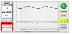
Figure 11: Graphic User Interface
Of course, for having a higher sampling precision, the same waveform can be actually taken from oscilloscope, shown in Figure 12. As expected, the circuit is able to drive the load maintain the desired current features over time and with the same theoretical behaviour of Figure 2.
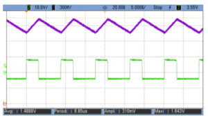
Figure 12: Output current (violet) and gate driver (green) Waveforms from oscilloscope
6. Conclusions
The presented DC-DC Buck Converter Variable-Tof f loop allows to precisely and smartly control the current features, returning a reliable car battery sourced driver. Other than the current peak, the loop is able to control the average current. Moreover, given (2), also the ripple is indirectly controlled. With respect to other solutions, the switching period is variable, intrinsically solving the instability issues. Indeed, the Ton changes with the input voltage while Tof f increases/decreases at each switching cycle accordingly to the comparison between Iavg and the target value, making (2) smaller/bigger (i.e. increasing/decreasing Iavg).
The system exploits an integrated low-side sensing resistor circuit to minimize the Printed Circuit Board usage space, avoiding extra pads to sense the current. To make the chip lighter and cheaper, the Buck Converter Cout has been neglected, as superfluous for the application.
The concept has been simulated with Simulink and then a more rigorous test has been conducted in laboratory with dSpace where worst condition simulations shown an excellent dynamic behaviour. The circuit appears to be robust, proving that sudden perturbations on Vin, Imax and Tof f do not upset the operation of the circuit. Compared to [8], the presented solution is lighter and works with an input voltage range of [4.5,27]V, able to drive a 3A LED with 500kHz maximum switching frequency, allowing extremely good average regulation precision and speed. A more detailed comparison of all Buck performances, including efficiency, with the state of the art is provided in [7].
Acknowledgment
A part of the work has been performed in the project iDev40. The iDev40 project has received funding from the ECSEL Joint Undertaking (JU) under grant agreement No 783163.
The JU receives support from the European Union’s Horizon 2020 research and innovation programme. It is co-funded by the consortium members, grants from Austria, Germany, Belgium, Italy, Spain and Romania.The information and results set out in this publication are those of the authors and do not necessarily reflect the opinion of the ECSEL Joint Undertaking.
- L. Dixon, “Average Current Mode Control of Switching Power Supplies,” 1999.
- O. Gasparri, R. Di Lorenzo, P. Del Croce, A. Pidutti, A. Baschirotto, “Vari- able off-Time Peak Current Mode Control (VoT-PCMC) as method for average current regulation in Buck Converter Drivers,” 2019.
- I. J. Prasuna, M. Kavya, K. Suryanarayana, B. Shrinivasa Rao, “Digital Peak Current Mode Control of Boost Converter,” 2014.
- Z. Jiuming, L. Shulin, “Design of slope compensation circuit in peak-current controlled mode converters,” 1310–1313, 2011.
- J. Ejury, Buck Converter Design, Infineon Technologies North America (IFNA), 2013.
- Fang, Chung-Chieh, Redl, “Subharmonic Instability Limits for the Peak-Current- Controlled Buck converter With Closed Voltage Feedback Loop,” Power Elec- tronics, 1085–1092, 2015.
- R. Di Lorenzo, O. Gasparri, A. Pidutti, P. Del Croce, A. Baschirotto, “On-Chip Power Stage and Gate Driver for Fast Switching Applications,” 2019.
- V. Anghel, C. Bartholomeusz, A. Vasilica, G. Pristavu, G. Brezeanu, “Variable Off-Time Control Loop for Current-Mode Floating Buck Converters in LED Driving Applications,” 2014.