Fabrication and Optimization of High Frequency ZnO Transducers for Both Longitudinal and Shear Emission: Application of Viscosity Measurement using Ultrasound
 , Ibrahim Zaaroura 2, Abbas Salhab 1, 3, Pierre Campistron 1, Julien Carlier 1, Malika Toubal 1, Souad Harmand 2, Vincent Thomy 4, Marc Neyens 3, Bertrand Nongaillard 1
Adv. Sci. Technol. Eng. Syst. J. 5(6), 1428–1435 (2020);
 DOI: 10.25046/aj0506173
This paper covers the study of high-frequency (~ 1 GHz) ZnO piezoelectric transducer integrated on a silicon substrate able to generate both compressional and shear acoustic waves. First, to promote the longitudinal mode, an electrical matching of the transducer in this high-frequency range is effectuated. Second, to promote shear waves, new deposition conditions were applied, giving thin zinc oxide films of inclined c-axis. The RF microprobe was used to validate the transducer design and to conduct the viscosity measurements. Thus, the shear and the volume viscosity of a water droplet were measured.
1. Introduction
This paper is an extension of work originally presented in the International Conference on Design & Test of integrated micro & nano-System (DTS 2019) [1]. Piezoelectric sensors have many applications in different areas, like the medical, manufacturing, and research fields [2-5]. One of these applications is the piezoelectric ZnO transducer, which has been well known for about 50 years, mainly for its high-frequency applications. [6]. Compared to monocrystalline lithium niobate (LiNbO3) [7], ZnO has lower piezoelectric performances (coupling coefficients), but it is easier to be deposited with the classical sputtering process. The thickness of the deposited ZnO can be from 10s nm to several microns. Additionally, it is possible to lead to the right (C-axis) crystallite orientation for longitudinal acoustic wave emission with a relatively short process duration.
Prior publications have demonstrated that depending on the distance between the sample’s axis and the sputtering target axis, the orientation of crystallites cannot be homogeneous over a large substrate surface [8]. The inclination of the C-axis can be modified by controlling this distance, which slightly increases the proportion of shear acoustic waves at the expense of compressional waves.
Only a few applications report using a transducer capable of generating longitudinal and shear acoustic waves simultaneously [9, 10]. The first step in this article is to present the manufacturing, the characterization and the electrical modeling of ZnO piezoelectric transducers that generate both shear and longitudinal waves in the solid. Then, an electrical matching was used in order to increase the longitudinal mode.
The deposition of layers with appropriate orientation for shear excitation has been mentioned in several articles using different methods and substrates [11-13]. Thus, to increase the shear mode, one of these methods, mainly based on the addition of a blind positioned between the sputtering target and substrate, was used. The growth of ZnO films with inclined orientation makes it possible to generate shear waves.
Finally, to demonstrate the usability of this transducer, both longitudinal acoustic reflection and shear coefficients at the solid/liquid interface were used to characterize the viscous fluid (a sessile water droplet) properties from its shear and volume viscosity.
2. Manufacturing, characterization and modeling of ZnO transducers
2.1. The manufacturing steps of the ZnO transducers
The piezoelectric material used is ZnO. It is deposited between two metal electrodes. The deposition configuration is shown in Figure 1, and it is fabricated by a standard thin-film technology: deposition and lift-off.
The choice of ZnO as a piezoelectric material can be related to its ease of preparation and its increased scope in high-frequency applications. One can site, for example, the acoustic microscopy applications in 100s MHz to 1s GHz frequency range [14,15].

Figure 1: Multilayer Diagram of a Piezoelectric Transducer.

Figure 2: Piezoelectric transducer fabrication steps.
The ZnO piezoelectric transducer’s fabrication starts with the deposition of 10 nm of a titanium layer by cathode sputtering on the surface of a 400 μm thick silicon wafer, followed by deposition of 80 nm of platinum. These two first layers will act as the lower electrode. A photolithography process is then performed to make the transducers pattern, where a thick 8 μm layer of PMGI SF19 (Microchem Corporation) is dispensed by spin coating on the lower electrode. Further, a layer of 1.5 µm of S1828 (Shipley Corporation) is appended. After ultraviolet exposure using a mask, a commercial developer MF 319 (Microposit) was used to obtain a pattern of different diameters in the PMGI layer. After that, a 2 μm thin ZnO layer was deposed. Finally, a 10 nm of titanium adhesion layer followed by 400 nm of gold were deposited. The gold layer is used to enable soldering of the contact electrode to a gold wire to connect the transducer to an external circuit. The last step is the lift-off process, where the UV exposed resin is removed to get the transducers pattern. The transducers have a diameter of 150 um. The microfabrication process is shown in Figure 2.
2.2. Characterization of the transducers
The ZnO transducers’ characterization is carried out by a Rohde & Schwarz ZVA8 Vector Network Analyzer (VNA) as shown in Figure 3.a. The electrical contact is made using a radio-frequency measuring tip Z-probe, GS type (pitch = 1.25 mm) connected by a coaxial cable to the VNA (Figure 3.b). Since we are working within a high-frequency range in a Gigahertz order, a calibration must be done before each measurement to ensure reliable results. The silicon sample is fixed by suction (using a vacuum pump) on a circular plate.

Figure 3: Image of (a) Rohde & Schwarz ZVA8 Vector Network Analyzer (VNA), (b) tip Z-probe.

Figure 4: (a) Parameter measured with the network analyzer, (b) Zoom around the longitudinal acoustic wave resonance.
The parameter as a function of frequency, shown in Figure 4.a, is the output measured on a transducer located on the edge of the substrate. At this position, the crystal orientation of the ZnO is not perfectly vertical, thus, the generation of acoustic shear waves is clearly observed. This parameter given by Equation 1 is composed of two contributions [16,17]. The first one comes from the direct reflection of the electric wave on the transducer ( . The second is a result of all the acoustic wave reflections on the opposite side of the substrate. These acoustic reflections are then converted into electrical signal by the transducer.
![]()
The coefficient K11 is the electro-acoustic-electrical coupling coefficient of the piezoelectric material used to convert energy from electric into acoustic for the emission then from acoustic into electrical for the reception.
The reflection transfer function of our system is represented by . To obtain the temporal response, an inverse Fourier Transform is performed (Figure 5). In the time domain, the electrical term response appears shortly after the transducer’s excitation while the acoustic term arises later.
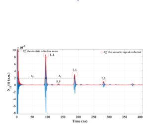
Figure 5: Impulse response for f = [0.2 – 1.6 GHz].
The response shown in Figure 4 exhibits a rapid oscillation of S11(f) having a peak oscillation around the central frequency (f = 0.9 GHz). This is due to the fact that for each wavelength emitted in the substrate of a given thickness, the superposition of the emitted and received waves occurs with a variable phase shift. Thus, the total vibration amplitude acquired by the transducer (amplitude of the sum of the emitted and received waves) is greater for the case when the two waves (incident and reflected) are in phase and lower when they are in opposite phases (phase cancellation effect). This phenomenon is portrayed by the SWR standing wave ratio (between the highest and the lowest vibration levels). The frequency of these periodic interference ripples in S11(f) is , where and are respectively the celerity of wave and the thickness of the silicon layer (400 µm) (Figure 4.b). The time-domain response corresponding to Figure 4.a is shown below in Figure 5. The multiple echoes are seen, the first one corresponding to the . This electrical echo is directly due to the electrical mismatch between the transducer and the external circuit (50-Ohm load impedance of the VNA). The minor delay corresponds to the electromagnetic wave propagation time in the cable portion between the network analyzer and the RF microprobe. The other echoes correspond to the different acoustic signals ( ) traveling back and forth in the silicon layer. They are separated by periods defined by the double Si wafer thickness’s propagation time.
It is observed that the transducer emits both longitudinal and shear waves, which propagate in the silicon substrate at different speeds. The waves are denoted LL and SS for longitudinal/longitudinal or shear/shear propagation, respectively. The coupling of these 2 waves is very weak as the reflecting surface of the silicon is smooth and parallel to the transducer.
2.3. Transducer design using Auld’s model
For checking the manufacturing quality of the transducers, we can model their impedance Zel and compare it to experiments. The piezoelectric layers being very thin compared to their lateral dimension (2 µm thick vs. 150 µm diameter), we can model them by a 1D model, like the Auld model [18].
As longitudinal and shear waves are emitted, we will use a modified Auld model that includes the two modes of emission. For that, it is necessary to consider the different mechanical impedances Z of the transducer’s constituting layers. The analytical formulation for Zel of a transducer rigidly bounded to a semi-infinite solid is given by Equation 2; the mechanical impedances and in Equations 3 and 4 are hardly significant or negligible relatively to the other terms [16].
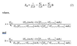
L and S indices stand to the longitudinal and shear waves. is the static capacitance of the ZnO transducer, the dielectric permittivity of ZnO, and SZnO are the thickness and the active surface of the ZnO layer. is the square of the electromechanical coupling coefficient of the ZnO. with the wave number in ZnO and the longitudinal or transverse wave’s velocity the ZnO.
From an experimental point of view, the S-parameter is linked to the transducer impedance as follows:
![]()
is the characteristic impedance of the network analyzer equal to 50 Ω.

Figure 7: Simulated (blue curve) and measured (red curve) electrical impedance of the 150 µm diameter ZnO transducer.
The 150 µm diameter ZnO transducer’s simulation results are shown in Figure 7 by the solid blue curves. The real part of (Figure 7.a) exhibits two peaks occurring at the resonance frequencies of the transverse ( = 0.38 GHz) and longitudinal ( = 0.9 GHz) waves.
A good fit between the simulation and the experimentation can be seen in Figure 7. So, the Auld model can be used to design a transducer for which the real part is close to 50 Ω by adjusting the thicknesses of the thin layers and the surface.
The manufacturing process is well calibrated which allows us to know the thicknesses of the different materials quite precisely. We were able, during various works, to measure the acoustic properties of ours deposited layers [17]. We therefore know the parameters on which the model depends, except the electro-mechanical coupling coefficients of the transducers which depend on the unknow orientation of the ZnO crystallites. We get them by an optimization routine using Nelder-Mead’s algorithm. In the simulation, Ks and KL were set to 0.10 and 0.23, respectively. The result of optimization for KL is close to the theoretical one obtained for a perfect crystallite c-axis alignment (KL = 0.27, according to [7]).
As shown in Figure 8, the pure electrical model we use represents the 2 modes of vibration of the transducer by the association of 2 RLC circuits shunted by the static capacitance . From a physical point of view, the capacity reflects the resonators electromagnetic behavior, while the two parallel resonant circuits exhibit the resonators acoustic behavior.
The electrical parameters of the circuit are determined by using the electrical impedance thanks to the measurement of the parameter. As for the evaluation of the coupling coefficients, we obtained the electrical parameters by an optimization procedure.
The electrical parameters of the circuit are determined by using the parameter:

Figure 8: The equivalent electric circuit of the ZnO transducer.
3. Transducer optimization
3.1. Increasing the longitudinal acoustic waves emission by impedance matching
In any kind of application, we need to favor either one or both types of the generated waves. In the present study, regarding the matching network, promoting the longitudinal waves is sought [19].
The concept of electrical matching is to transfer the maximum power from the source to the transducer or, in other words, to eliminate electrical reflections on the transducer in a chosen frequency range. As piezoelectricity is a reciprocal phenomenon, the electrical matching network also acts as an acoustical matching layer. So, the electrical matching reduces the reflection of the acoustical waves returning on the piezoelectric layer, which increases the acoustical transmission coefficient at the piezoelectric device. Simultaneously, levels of both acoustic waves propagating in the device and electrical measurement signal increase.
There are two steps for the electrical impedance matching. The first one consists of connecting the transducer with a gold wire (25 µm of diameter). The second step uses an L-section impedance matching [20], consisting mainly of two reactive elements (capacitor and inductor). The capacity is used to adjust the real part of the impedance to 50 Ω, while the coil reduces the imaginary part. A capacitance has a significant loss effect at high-frequency, causing critical insertion losses [21]. For this reason, a chip inductor with a value of 8.6 nH was put in series with the load (transducer connected by the gold wire) at = 1.12 GHz. The real part of the load at this frequency is equal to 50 Ω.
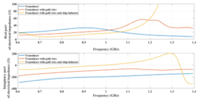
Figure 9: The real and imaginary parts of the electrical impedance of the ZnO transducer (blue curve), the transducer with gold wire (red curve) and transducer with gold wire and chip inductor (yellow curve).
It is clearly seen that the electrical response has been modified (Figure 9). This modification can be related to the losses and the parasite impedances of bonding wire and packaging. So, it has become complicated to choose a filter based on the equivalent electric circuit of the transducer, such as the Butterworth or Chebychev filters [22, 23, 24]. Therefore, the simplest solution is to use the transducer impedance’s real and imaginary parts, including the wire.

Figure 10: Image of the different elements of the circuit.
The expected result is the gain in longitudinal wave amplitude, which will make it easy to connect the transducer to the VNA or a generator via an SMA connector, as shown in Figure 10.
To verify that the electrical adaptation works as expected, we compare the insertion loss of the transducer before and after the adaptation, through an SMA connector. Afterwards, the responses in terms of received amplitude level will be compared. The electrical insertion losses was calculated by the following equation:
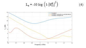
Figure 11: Measured electrical insertion losses.
As shown in Figure 11, the electrical adaptation has reduced the insertion losses. The matched transducer exhibits an amplitude gain of 8 dB and a bandwidth enlarged to 250 MHz.

Figure 12: Impulse response , (a) the electrical reflection (b) the acoustic response .
The matching network’s direct effect can be represented in Figure 12, showing the echoes before (blue curve) and after (red curve) the electrical matching. The attenuation of the reflected electrical signal is notably due to the conversion from electrical into acoustic energy. This conversion can be seen by the simultaneous amplitude decrease of the electrical echo (Figure 12.a) and the increase of the first acoustical echo (Figure 12.b). However, this result only applies to .
Although the electrical adaptation improves the transducer’s acoustic sensitivity, the electrical reflection does not completely disappear because the use of an inductor is only at a single frequency and not over the bandwidth of the transducer.
3.2. Increasing the shear acoustic waves emission by deposition of ZnO inclined c-axis by R.F. magnetron sputtering
It appears difficult to use a matching network for increasing the level of shear waves as they are too weak. Previous measurements have been made with a transducer from a misaligned area (with respect to the ZnO target of the silicon wafer). By increasing that effect, it is possible to increase the shear level.
The ZnO thin film fabrication process was modified to balance the amplitude of generated longitudinal and shear waves by changing the material crystalline orientation. The film was deposited on three wafers with the following stack: Pt (80 nm) / Ti (10 nm) / Si (400 µm) by R.F. magnetron sputtering technique. The substrate was fixed in the chamber, whose total pressure was 0.02 mBar. A rectangular cover (the blind) is positioned between the target and the substrate, making it possible to obtain oblique incidence of the particles in order to locally influence the growth of the ZnO thin film (Figure 13). The blind was made of aluminum, had a height of 30 mm and a thickness of 1 mm. It was placed in the center of the substrate. The deposition rate of the ZnO films varied from 15 to 25 nm/min.
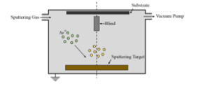
Figure 13: R.f. magnetron sputtering system with additional blind between substrate and target.
A cross-section SEM image of the ZnO deposited on the silicon substrate is shown in Figure 14. The inclination of the crystallite orientation is approximately 14.5° to the surface normal can be observed. So, shear and longitudinal waves can be excited. However, the inclination of the crystal orientation is strongly dependent on the distance between the blind and the transducer (in the substrate plane); therefore, the c-axis inclination will be higher in an area close to the blind or close to the edge of the substrate.
Figure 15.a shows the resonance diagram of the piezoelectric transducer; two distinguished downward peaks can be seen, the first one in the frequency range [0.35 – 1 GHz] which corresponds to critical transversal waves response compared to Figure 4 and the other peak in the range [1 – 2 GHz] corresponding to longitudinal waves response. Two oscillations with different frequencies ∆f = {S: 7.4 MHz, L: 10.5 MHz}, are presented in Figure 15.b. Each of them presents a different wave mode. This result directly reflects the transducers’ ability sputtered with the inclined ZnO c-axis to generate both shear and longitudinal waves.

Figure 14: Cross-sectional SEM image of ZnO film with c-axis inclined of 14.5°.

Figure 15: Impulse response , (a) for f=[0.35 – 2 GHz], (b) Zoom around the longitudinal and the shear acoustic waves resonance.
Figure 15 (b), as we expect each of them are close to the theoretical ones {Cs/2e = 5843/800e-6 = 7,3 MHz and Cl/2e = 8432/800e-6 = 10,54 MHz}.
The time-domain representation is used below to check the level of both signals. Figure 16 shows the inverse Fourier transform of the S11 parameter. For [0.35 – 2 GHz], two different acoustic reflections LL, and SS, are the responses from the generated acoustic waves, with LL being a purely longitudinal response with longitudinal wave emitted and the longitudinal wave reflected. The longitudinal speed of sound in silicon (8432 m/s) is greater than the transversal one (5832 m/s); thus, the time of reception of the signal for the longitudinal waves should be the fastest (the first reflection on Figure. 16.a corresponds to LL). The second impulse SS is the purely transversal reflected signal with the time delay being significantly greater than LL. For a bandwidth of 1.65 GHz, the ratio of the shear wave to the longitudinal wave is 0.5.
We decreased the frequency range to [0.35 – 1 GHz] (Figure 16.b), the shear to shear (SS) reflection amplitude increases, and the longitudinal to longitudinal (LL) amplitude decreases, which what was expected to be seen since the lower frequency range favors the transversal waves (Figure 16.a). The ratio of shear to longitudinal amplitudes increases to 2.6.
For f = [1 – 2 GHz] (Figure 16.c), the result is the profound decrease in the SS reflection amplitudes and the profound increase in the LL amplitudes, which is what to expect since the high frequencies favor the longitudinal waves. We now have a ratio of shear to longitudinal amplitudes decreased to 0.01.
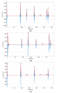
Figure 16: Impulse response , the time delays and between them corresponds to the propagation delays of the longitudinal and transverse wave travelling twice the thickness of the wafer. (a) f = [0.35-2 GHz], (b) f = [0.35-1 GHz] and (c) f = [1-2 GHz].
Levels are weak, but all signals are out of the noise and can be used for measurements. If necessary, they can be increased using a convenient matching network, as demonstrated in part 1. Thus, we propose a method allowing the emission of both longitudinal and shear waves using only one fixed fabrication process. However, the c-axis tilt is not the same on the wafer surface, so the transducers cannot generate the same wave level for each frequency range, so the ratio of shear to longitudinal amplitudes changes.
4. Application: Measurement of the viscosity of a liquid using both longitudinal and shear waves generated by the ZnO transducer
There are a vast number of applications that utilize physical parameters in relation to acoustic waves-material interactions. An application to measuring the fluid viscosity is presented below to demonstrate the usability of the proposed transducer design. Water is used as the reference fluid whose acoustic properties are given in [25, 26].
The total viscosity of water can be extracted from the shear and longitudinal waves generated at the liquid/ solid interface [27,28]. Our transducers can generate these two types of waves. We used the evaporation of 1 µL droplet of water to determine the two kinds of viscosities (namely shear and volume viscosities). The dynamic shear viscosity was extracted using the shear wave, while the volume viscosity from both waves.

Figure 17: Incident acoustic waves interaction at droplet/silicon interface.
Figure 17 presents the direct contact of the acoustic waves to the water droplet/silicon interfaces. The acoustic waves reflect at the interface and generate two components, i.e., longitudinal and shear reflected waves.
Several mechanical properties at the silicon/water interface influence the measurement, and these are also strongly dependent on the temperature. The reflection coefficient at the solid/fluid interface is given by equation 5, Z0 is the mechanical impedance of the silicon, considered purely elastic, so Z0 is purely real [29], while water presents viscoelastic properties. As a consequence, its acoustic impedance is in a complex form.
![]()
where , is the density of the medium, and is the acoustic velocity of the wave propagating inside of the medium. The reflection coefficients are determined for both longitudinal and shear reflected waves. So, the complex form of the shear reflection coefficient ( *) and the longitudinal reflection coefficient ( *) are shown in the Equations 6 and 7. These coefficients give access to the modulus and the phase angle of the two reflections acoustic wave at the interface.
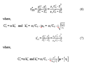
where , are the complex longitudinal and shear velocity of water, is the density, , the complex longitudinal and shear wave number, ω (rad/s) the angular velocity. and are the shear and volume viscosity, respectively.
and are the effective longitudinal and shear phase velocities in water respectively, is the shear attenuation. The kinetics of the shear and volume viscosity is shown in Figure 18. A sessile droplet of water evaporating at room temperature of 25°C is used. It is clearly seen that the consistency of the theoretical and experimental results.

Figure 18: Kinetics of the shear and volume viscosity of a water droplet at T=25°C compared to the reference values.
It was essential to improve the shear waves emission to accurately measure the shear viscosity values for different complex fluids such as nanofluids. These nanofluids contain nanoparticles in suspension in a matrix fluid; that is why it is important to have a high sensitivity of these particles that settled above the surface.
5. Conclusion
This article is the extended version of a paper published in IEEE Xplore. We have studied the fabrication and the optimization of a ZnO high-frequency transducer able to generate both longitudinal and shear waves. To model the transducer’s electrical response, we used the Auld model; we noticed a good agreement between electrical impedance measurements and simulations, allowing its use in the design of transducers. To improve the sensitivity, we have used an electrical circuit including a chip inductor and an SMA connector so that it could be used without the requirements of an external RF microprobe. This matching circuit had been experimented with for the longitudinal mode and allowed us to gain ~ 8 dB on the electrical insertion losses.
In order to increase the shear wave level, the growth of ZnO films with tilting of the crystallite axis has been achieved using a blind of 10 mm that was positioned between the target and the substrate during the R.F. magnetron sputtering. The inclination of the crystal orientation was approximately 14.5°.
Both shear and longitudinal waves can be excited with this multi-mode transducer; the wave type can be selected by adjusting the emission frequency.
As to proof of the usability of this kind of measurement, an application has been proposed. We have exploited the simultaneous measurements of the two types of waves to extract both shear and volume viscosities of the water. Comparisons between the experimental and theoretical results show a good agreement.
Conflict of Interest
The authors declare no conflict of interest.
Acknowledgment
This work was partially supported by the French Renatech network. A part of the cost has also been supported by STMicroelectronics and Hauts-de-France region. The authors wish to thank all the members of the cleanroom at IEMN- UMR CNRS 8520. They are also grateful to the professor Bertrand Nongaillard for his encouragement and support in this work. Finally, the authors also thank the laboratory engineers, Dr. Malika Toubal, and Dr. Nikolay Smagin, for their help in preparing the article.
- H. Dahmani, I. Zaaroura, P. Campistron, J. Carlier, M. Toubal, B. Nongaillard, “Study of a dual longitudinal and shear acoustic wave ZnO transducer in the gigahertz frequency range: Application to viscosity measurement and first step for device integration,” in IEEE International Conference on Design and Test of Integrated Micro and Nano-Systems, DTS 2019, 2019, doi:10.1109/DTSS.2019.8914906.
- F.L. Di Scalea, H. Matt, I. Bartoli, A. Srivastava, G. Park, C. Farrar, “The fundamental response of piezoelectric guided-wave sensors and applications to damage and impact location,” in Proceedings of the 3rd European Workshop – Structural Health Monitoring 2006, 1271-1280, 2006.
- C. Caliendo, “Longitudinal modes along thin piezoelectric waveguides for liquid sensing applications,” Sensors (Switzerland), 15(6), 12841-12856, 2015, doi:10.3390/s150612841.
- L.P. Suwal, R. Kuwano, “Disk shaped piezo-ceramic transducer for P and S wave measurement in a laboratory soil specimen,” Soils and Foundations, 53(4), 510-524, 2013, doi:10.1016/j.sandf.2013.06.004.
- F.A. Alexandre, P.R. Aguiar, R. Götz, M.A.A. Viera, T.G. Lopes, E.C. Bianchi, “A novel ultrasound technique based on piezoelectric diaphragms applied to material removal monitoring in the grinding process,” Sensors (Switzerland), 19(18), 2019, doi:10.3390/s19183932.
- J. de Klerk, “Thin film zinc oxide transducers for use in microwave devices,” Ultrasonics, 8(3), 159-164, 1970, doi:10.1016/0041-624X(70)90614-1.
- D. Royer, E. Dieulesaint, Elastic Waves in Solids I: Free and Guided Propagation, translated by D. P. Morgan, 2000.
- M. Link, Study and realization of shear wave mode solidly mounted film bulk acoustic resonators (FBAR) made of c-axis inclined zinc oxide (ZnO) thin films: application as gravimetric sensors in liquid environments, Ph. D Thesis, Henri Poincaré University, 2006.
- I. Zaaroura, M. Toubal, H. Reda, J. Carlier, S. Harmand, R. Boukherroub, A. Fasquelle, B. Nongaillard, “Evaporation of nanofluid sessile drops: Infrared and acoustic methods to track the dynamic deposition of copper oxide nanoparticles,” International Journal of Heat and Mass Transfer, 127, 1168-1177, 2018, doi:10.1016/j.ijheatmasstransfer.2018.07.102.
- C. Virgilio, Caractérisation du mouillage de surfaces micro / nanostructurées par méthode acoustique haute fréquence: application aux traitements humides dans l’industrie de la microélectronique Ph. D Thesis, Valenciennes and Hainaut-Cambresis University, 2017.
- M. Link, M. Schreiter, J. Weber, R. Primig, D. Pitzer, R. Gabl, “Solidly mounted ZnO shear mode film bulk acoustic resonators for sensing applications in liquids,” IEEE Transactions on Ultrasonics, Ferroelectrics, and Frequency Control, 53(2), 492-496, 2006, doi:10.1109/TUFFC.2006.1593389.
- S. Bensmaine, L. Le Brizoual, O. Elmazria, J.J. Fundenberger, B. Benyoucef, “Deposition of ZnO inclined c-axis on silicon and diamond by r.f. magnetron sputtering,” in Physica Status Solidi (A) Applications and Materials Science, 204(9), 3091-3095, 2007, doi:10.1002/pssa.200776322.
- M. Link, M. Schreiter, J. Weber, D. Pitzer, R. Primig, M.B. Assouar, O. Elmazria, “C-axis inclined ZnO films deposited by reactive sputtering using an additional blind for shear BAW devices,” in Proceedings – IEEE Ultrasonics Symposium, 1, 202-205, 2005, doi:10.1109/ULTSYM.2005.1602831.
- K. Yamada, H. Shimizu, M. Minakata, “PLANAR-STRUCTURE FOCUSING LENS FOR OPERATION AT 200 MHZ AND ITS APPLICATION TO THE REFLECTION-MODE ACOUSTIC MICROSCOPE.,” in Ultrasonics Symposium Proceedings, 745-748, 1986, doi:10.1109/ultsym.1986.198834.
- B.T. Khuri-Yakub, “Scanning acoustic microscopy,” Ultrasonics, 31(5), 361-372, 1993, doi:10.1016/0041-624X(93)90070-G.
- Y. Deblock, P. Campistron, M. Lippert, C. Bruneel, “Electrical characterization of plate piezoelectric transducers bonded to a finite substrate,” The Journal of the Acoustical Society of America, 111(6), 2681-2685, 2002, doi:10.1121/1.1416904.
- P. Campistron, J. Carlier, N. Saad, J. Gao, M. Toubal, L. Dupont, G. Nassar, B. Nongaillard, “High frequency ultrasound, a tool for elastic properties measurement of thin films fabricated on silicon,” in Advanced Materials Research, 324, 277-281, 2011, doi:10.4028/www.scientific.net/AMR.324.277.
- B.A. Auld, R.E. Green, Acoustic Fields and Waves in Solids: Two Volumes, Physics Today, 1974.
- J. Gao, J. Carlier, S. Wang, P. Campistron, D. Callens, S. Guo, X. Zhao, B. Nongaillard, “Lab-on-a-chip for high frequency acoustic characterization,” Sensors and Actuators, B: Chemical, 177, 753-760, 2013, doi:10.1016/j.snb.2012.11.037.
- D.M. Pozar, Microwave Engineering, 4th Edition, 2012.
- R. Fiore, “Capacitors in broadband applications,” Applied Microwave and Wireless, 13(5), 40, 2001.
- R.N. Thurston, “Effect of Electrical and Mechanical Terminating Resistances on Loss and Bandwidth According to the Conventional Equivalent Circuit of a Piezoelectric Transducer,” IRE Transactions on Ultrasonic Engineering, 7(1), 16-25, 1960, doi:10.1109/T-PGUE.1960.29256.
- D.C. Youla, A new theory of broadband matching, IEEE Transactions on Circuit Theory, 1964.
- W.-K. Chen, The Circuits and Filters Handbook, 2003.
- L. Korson, W. Drost-Hansen, F.J. Millero, “Viscosity of water at various temperatures,” Journal of Physical Chemistry, 73(1), 34-39, 1969, doi:10.1021/j100721a006.
- R.A. Horne, D.S. Johnson, “The viscosity of water under pressure,” Journal of Physical Chemistry, 70(7), 2182-2190, 1966, doi:10.1021/j100879a018.
- J. Holmes, G. Parker, W. Povey, “Temperature dependence of bulk viscosity in water using acoustic spectroscopy,” in Journal of Physics: Conference Series, 269(1), 2011, doi:10.1088/1742-6596/269/1/012011.
- A.J. Zuckerwar, R.L. Ash, “Variational approach to the volume viscosity of fluids,” Physics of Fluids, 18(4), 2006, doi:10.1063/1.2180780.
- M. Trempa, C. Reimann, J. Friedrich, G. Müller, D. Oriwol, “Mono-crystalline growth in directional solidification of silicon with different orientation and splitting of seed crystals,” Journal of Crystal Growth, 351(1), 131-140, 2012, doi:10.1016/j.jcrysgro.2012.04.035.