
Solution of the Semiconductor-Device Equations by the Numerov Process
Volume 5, Issue 6, Page No 1414-1421, 2020
Author’s Name: Nicolò Speciale1, Rossella Brunetti2, Massimo Rudan1,a)
View Affiliations
1DEI Department, University of Bologna, Viale del Risorgimento 2, I-40136 Bologna, Italy
2FIM Department, University of Modena and Reggio Emilia, Via Campi 213/A, I-41125 Modena, Italy
a)Author to whom correspondence should be addressed. E-mail: massimo.rudan@unibo.it
Adv. Sci. Technol. Eng. Syst. J. 5(6), 1414-1421 (2020); ![]() DOI: 10.25046/aj0506171
DOI: 10.25046/aj0506171
Keywords: Numerov Process, Modeling Charge Transport, Solid-State Devices

Export Citations
The one-dimensional form of some types of differential equations that appear in the modeling of solid-state devices, like, e.g., the Poisson and Schro¨ dinger equations, can be solved numerically using the Numerov Process (NP). The accuracy of NP is superior by at least two orders of magnitude to that of commonly-used solution methods like, e.g., the finite-difference one. Another advantage of NP is that the increase in computational cost is modest. This paper investigates the possibility of extending the applicability of NP to the whole set of equations that constitute the mathematical model of semiconductor devices. It shows that the charge-continuity and charge-transport equations can be recast in a form suitable for NP. The performance of the method is tested on an n+-n-n+ device, and the extension of the approach to the two-dimensional transport problem is worked out.
Received: 30 June 2020, Accepted: 12 October 2020, Published Online: 16 December 2020
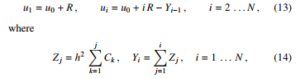
1. Introduction
A number of physical problems are described by second-order differential equations of the form
![]()
(primes indicate derivatives with respect to x). When a uniform grid with grid size h is used, such a form can be tackled numerically, thanks to the absence of the first derivative, with an O(h4)-accurate discretization method generally known as Numerov Process (NP); this in contrast to O(h2) of the finite-difference method (the derivation of the scheme is shown in the Appendix). Linearization of (1) yields
![]()
Scope of this paper is to extend the applicability of NP to the system of equations that describe the transport of electric charge in solid-state devices. This paper is an extension of work originally presented at the SISPAD 2019 Conference [1]; besides the Appendix, more details about NP are given, e.g., in [2] and references therein.
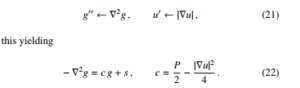
In some cases, (2) can be reduced to equations that appear in the model for semiconductors; for instance, letting Q = 0, and naming z = u the electrostatic potential normalized to the thermal voltage kB T/q, and P = q/(εkB T)%, with % the charge per unit volume, transforms (2) into the Poisson equation, which is one of the equations of the standard semiconductor-device model (in the above definitions, symbols q, ε, kB, T denote the elementary charge, material permittivity, Boltzmann constant, and lattice temperature, respectively). If, instead, one lets P = 0, the form of the timeindependent Schrodinger equation is recovered, which enters the¨ semiconductor-device model when nanometer-scale devices are considered; in this case, z = w is the time-independent wave function, whereas the form of Q reads Q = 2m(E − V)/~2, where E = const is the total energy of the electron and V(x) the potential energy; in turn, m is the electron effective mass and ~ the reduced Planck constant.
The elimination of the odd-order derivatives in the Taylor expansion (see Appendix), as required by NP, prescribes the use of a uniform grid; the better accuracy of the method largely compensates for this aspect. An application of NP to the analysis of a semiconductor device was shown in [2], where the coupled solution of the Schrodinger-Poisson system was dealt with; in that case, no¨ manipulation of the equations was necessary because both have already the form (2).
Object of this paper is to show that, by a suitable choice of the unknowns, NP can be extended to the whole set of equations constituting the mathematical model of semiconductor devices. To this purpose it is convenient to briefly outline the recent progresses in modeling, following the semiconductor-device roadmap (now “International Roadmap for Devices and Systems — IRDSTM” [3]) and the corresponding evolution of the mathematical models.
The standard model of semiconductor devices (drift-diffusion model) is made of the Poisson equation and, for each type of mobile charges (electrons and holes), of the continuity and transport equations for the mobile-charge density; the transport equation has two terms: the first one is of the drift type, the second one of the diffusive type. For submicron devices the model is extended by adding another pair of continuity and transport equations, whose unknown is the energy density of the carriers (in this case, the model is termed hydrodynamic).
When the lateral extension of the device channel shrinks to the nanometer scale, the device can be described as a cylindrical structure. This makes it possible to separate the longitudinal and transversal directions; then, the calculation of the charge density is accomplished by solving the Schrodinger equation over each cross¨ section, whereas the analysis along the longitudinal direction is still carried out in classical terms. An example is found in the solution of a cylindrical nanowire shown in [2]. Other examples of nanometersize structures made of compound materials are illustrated in [4].
The n+–n–n+ structure considered in this paper is suitable for checking the extension of NP to the solution of the whole transport model of semiconductors. The structure is one of the benchmarks used in the literature (see, e.g., [5] and references therein): besides being one-dimensional, like a nanowire or a gate-all-around transistor, it has the advantage of being unipolar, namely, for its description it suffices to use only one type of carriers (electrons in this case), thus halving the number of continuity-transport pairs of equations to be solved.
The investigations on numerical methods for solving the semiconductor equations have gone in parallel with the strong development of the integrated-circuit technology of the last 50 years. At present, the most successful solution techniques for the driftdiffusion or hydrodynamic models are incorporated in huge deviceanalysis systems, whose update and maintenance is a concern of the semiconductor Companies in cooperation with specialized Software Houses. The advantage of NP is that it is applicable to the existing solution techniques without excessive changes in the organization of the software, and with a limited increase in the computational cost; for this reason, also considering the improvement in accuracy, the application of NP to the semiconductor equation is worth considering. The present investigation about the applicability of NP to the numerical solution of the semiconductor transport equations considers the drift-diffusion model for the sake of simplicity, since the hydrodynamic model and the other models of higher order, derived from the Boltzmann Transport Equation, have the same structure.
The paper is organized as follows: the model equations are shown in Section 2 along with the transformation that gives them an NP-suitable form; the NP-based discretization in the onedimensional case is carried out in Section 3. A method for calculating the electric potential at each node independently of the coupling with the transport equation is outlined in Section 4, followed by a stability analysis of the iterative solution (Section 5). The results are shown in Section 6, and the extension of the method to the two-dimensional case, still over a uniform grid, is given in Section 7. Finally, the conclusions are drawn in Section 8, while a summary of the derivation of NP is provided in the Appendix.
2. Model Equations
The semiclassical, drift-diffusion equations describing the transport of carriers in solids is made of the Poisson equation and, for each type of charges (namely, electrons and holes), of a pair of equations made of the continuity and of the transport equations. Here a onedimensional device of the unipolar type is analyzed, whose carriers are electrons. This situation is found, e.g., in n+–n–n+ structures like that shown in Figures 1 and 2, or in memory devices of the phasechange type (e.g., [6, 7]); in these devices, the Poisson equation reads

Figure 1: Lateral view of the simulated n+–n–n+ structure. The red regions indicate the contacts, while the shades of green mimic the non-uniform dopant concentration.
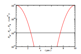
Figure 2: Dopant profiles of the simulated n+–n–n+ structure.
![]()
with n the electron concentration and ND(x) the concentration of ionized donors within the n+–n–n+ structure (when phase-change materials are considered, ND is replaced with the concentration nT of empty traps). The continuity equation of the electrons, and the corresponding drift-diffusion equation for the electron-current density read, respectively,
![]()
with U = U(n), Dn being the net-recombination rate and the electron-diffusion coefficient, respectively (here a constant value of Dn is considered). Combining (4) yields
![]()
The Wronskian determinant of the homogeneous equation associated to (5) reads, by Abel’s identity, W = const × exp(u) , 0.
The system of equations to be solved is then made of (3) and (5), whose boundary conditions are the values of u and n at the two ends of the (finite) integration interval. If the discretization of the interval produces N internal nodes, the boundary conditions are u0, uN+1 and n0, nN+1, respectively; in the analysis of solid-state devices it is assumed that the contacts force a condition of electric neutrality, so that n0, nN+1 are such that P0 = PN+1 = 0 (compare with (3)).
In a decoupled solution scheme, one assumes that n is given and solves (3) for u, then solves (5) for n using the form of u thus found; the procedure is iterated until convergence is reached. One notes that NP is not applicable to (5) as it stands, due to the presence of the first derivative; to give the equation a more suitable form one defines
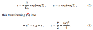
Transformation (6) does not consist in a reduction to a self-adjoint form; in fact, the expression of the latter would be
![]()
transformation (6) is not either an “exponential fitting” of the type commonly adopted for solving the semiconductor equations: the exponential fitting would in fact yield
![]()
where the current density Jn is approximated with a different constant along each interval between two nodes (in the field of
semiconductor-device modeling the scheme based on (9) is also known as Scharfetter-Gummel method [8]).
The homogeneous equation corresponding to (7) reads g00+cg =
0; in the iterative procedure by which the system made of (3) and (7) is solved within the finite integration interval, coefficient c is obtained from the electron concentration n and the normalized electrostatic potential u calculated at the previous iteration. As neither n nor u have poles, all points within the integration interval are ordinary.
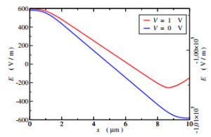
Figure 3: Electric field in the simulated n+–n–n+ structure, at different values of the applied bias; namely, 0 V (blue curve, left scale) and 1 V (red curve, right scale).\
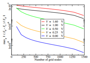
Figure 4: Maximum modulus of the relative variation maxg|(Ed − Ec)/Ed| of the electric field with respect to the densest grid (2000 nodes). The horizontal axis shows the number of nodes of each grid used in the comparison (more details are given in Section 6). The analysis has been repeated for different values of the applied voltage V, as shown in the inset.
3. Application of NP
In this Section, the Numerov Process is applied to (3) and (7) over a grid made of N, uniformly-spaced internal nodes with element size h. The Poisson equation (3) is transformed into the N × N algebraic system
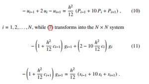
The matrix of the algebraic system (10) is symmetric, whereas that of (11) is non symmetric due to terms ci−1 and ci+1 at the left hand side. Although in the latter system the unknowns are gi = ni exp(−ui/2), terms ci and si still depend on the original unknown n; also, each gi depends, through exp(−ui/2), on the (arbitrary) zero of the electric potential; finally, due the presence of the exponentials of the electric potential, the matrix of the coefficients of (11) may become stiff. For the above reasons it is convenient to multiply both sides of (11) by exp(ui/2). In this way, the following replacements are carried out in (11): gi−1 ← ni−1 exp[(ui − ui−1)/2], gi ← ni, and gi+1 ← ni+1 exp[(ui − ui+1)/2]; by the same token, si−1 ← −(Ui−1/Dn) exp[(ui − ui−1)/2], si ← −(Ui/Dn), and si+1 ← −(Ui+1/Dn) exp[(ui − ui+1)/2].
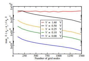
Figure 5: Maximum modulus of the relative variation maxg|(nd − nc)/nd| of the electron concentration with respect to the densest grid (2000 nodes). Compare with Figure 4.
The new form of (11), where the original unknown appears, is preferable because the exponents bearing differences like, e.g., ui − ui−1, instead of a nodal potential alone, are expected to be relatively small. To complete the calculation it is necessary to express the derivative u0 that appears in (7); this is also done using NP, so that the accuracy of the scheme is preserved, and yields
![]()
When i = 2,… N − 1, only the indices of internal nodes appear in
(12); if, in contrast, i = 1 or i = N, then one boundary condition is present (u0 and P0 = 0 or, respectively, uN+1 and PN+1 = 0); the last possible case occurs when i = 0 or i = N + 1, in which the values of the electric potential and charge in the interior of the contacts appear in (12); remembering that the contacts are equipotential and neutral, it is u−1 = u0, P−1 = 0 and uN+2 = uN+1, PN+2 = 0.
4. Decoupling the Model Equations
The model equations are solved by iterating between (10) and (11). In general, equations like these are tackled with algebraic solvers able to provide the values of the unknowns in a given sequence; for instance, considering the solution of (10) obtained through the A = LU decomposition, the ith nodal value of the normalized electric potential u is obtained only after calculating it at nodes 1 through i−1 (or at nodes N through i+1). Here a different approach is adopted, in which ui is obtained as soon as necessary, without the need of calculating its other nodal values. Such a result is achievable for the discretized form (10) of the Poisson equation by solving it with the scheme of [9, p. 769], that provides each nodal value ui independently of the others; using such a scheme after indicating with Ci the right hand side of (10) yields
![]()
The differences that appear in (11) after carrying out the replacements outlined above, are easily evaluated from (13–15): ui − ui−1 = R − Zi−1 , ui+1 − ui−1 = 2R − (Zi−1 + Zi).
In practice, this scheme decouples (10) from (11); it may appear that this result is due to the discretization: in fact, one can also eliminate the Poisson equation prior to the discretization, by recasting it in integral form [9, p. 781–784]. The calculation of the overall number of operations also shows that the method based on (13–15) requires fewer operations than the A = LU decomposition; specifically, for a matrix of order N the number of operations required by the A = LU decomposition is 6(N − 1) multiplications and
3(N − 1) additions, whereas the method based on (13–15) requires N − 1 multiplications and 4(N − 1) additions.
Another difference between the standard discretization schemes like, e.g., finite differences, and the present one is the following: here, the discretized functions and their derivatives of all orders “belong” to the nodes; as a consequence, no hypothesis is necessary about the form of the discretized functions over each element. In the finite-difference scheme the functions and their derivatives of even order belong to the nodes, whereas the derivatives of odd order belong to the elements.
5. Stability
Observing that the equations of the model are non linear, it is necessary to implement an iterative solution. Specifically, considering for instance the equilibrium case, the normalized charge concentrations Pi−1, Pi, Pi+1 at the right hand side of (10) depend on the electric potential u; the dependence is exponential in a non-degenerate semiconductor, or via a Fermi integral in a degenerate one [9]. In both cases, the derivatives dPi/du are negative irrespective of the type of carriers (electrons or holes) that is considered: in fact, electrons (holes) contribute negatively (positively) to the charge density, and the electron (hole) concentration increases (decreases) when u increases. This reasoning also applies in the non-equilibrium case, because the functional dependence of the concentration on the electric potential is the same. In conclusion, linearizing (10) with respect to u adds weight to the main diagonal of the system matrix, resulting in an improved convergence rate; this behavior, typical of the linearized Poisson equation in semiconductors, is due to the dependence of the carrier concentrations on the electrostatic potential and is common to a number of discretization schemes. In contrast, as shown below, the properties of the algebraic system obtained by discretizing the continuity and transport equations with the scheme shown in this paper are quite different from those obtained with the standard scheme.
Coming now to (11), when the expressions of ci−1, ci, ci+1 that appear in (7) are replaced in (11), one finds an algebraic system whose right hand side, in the ith row, is made of three summands: the structure of the first summand, Ai = −gi−1 + 2gi − gi+1, is the same as that of Poisson’s equation (10). The form of the other two terms is
![]()
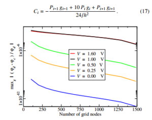
Figure 6: Maximum modulus of the relative variation maxg|(ϕd − ϕc)/ϕd| of the electric potential with respect to the densest grid (2000 nodes). Compare with Figures 4 and 5. The curves corresponding to V = 1.0 V and V = 1.6 V practically coincide.

Figure 7: Number of calls to the solver that are necessary to bring the error below a prescribed value, for a given number of grid nodes. Here a 1500-node grid was used. The curves refer to the bias values shown in the inset.
The coefficients defined by (16) are non negative, therefore they add weight to all diagonals of the system matrix (11); due to factor 10, the weight added to the main diagonal is generally dominant, unless node i is near an extremum of u. As for (17), the presence in it of the normalized charge density P, which may have either sign, makes the analysis more complicated; on the other hand, (17) is of order 2 in h, whereas, due to a cancellation that takes place when (12) is replaced in (16), Bi is of the same order as Ai, namely, order 0 in h. In essence, the structure of the algebraic system (11) deriving from the present discretization scheme of the continuity and transport equations is similar to that deriving from the Poisson equation. In contrast, the standard exponential-fitting scheme for the continuity and transport equations, based on (9), approximates U as a piecewise-constant function at each node, and linearizes u between each pair of nodes; with these premises, the scheme yields
![]()
whose coefficients Kkj depend on the normalized electric potential through the Bernoulli function B:
![]()
Besides the approximations mentioned above, it is easily found that the main diagonal of the algebraic system (18) is not necessarily dominant [9, p. 781].
6. Results
As an example of application, the solution scheme based on NP is applied here to the n+–n–n+ structure whose lateral section and dopant profiles are shown in Figures 1 and 2, respectively. The device length is L = 10 µm, the concentration of the light, constant dopant (black line in Figure 2) is NB = 1015 cm−3, while the two profiles (red lines) are given by NL = N0 exp(−x2/x02) and NR = N0 exp[−(L − x)2/x02], with N0 = 1017 cm−3 and x0 = 1.165 µm, respectively. The total dopant distribution to be used in (3) is ND(x) = NB + NL + NR. The device is uniform in the direction normal to the field; the equations of the models have been solved at different applied voltages V, ranging from equilibrium (0 V) to 1.6 V. The form of the electric field E is shown in Figure 3 for V = 0 V and V = 1 V.
Each solution was repeated on different grids, starting with a reference grid having N = 2000 nodes and successively decreasing it down to N = 100. Figure 4 compares the electric field E calculated using the 2000-node grid with that calculated using coarser grids. As all grids are obtained by refining the 100-node one, for each node of the latter there exists a node of the denser grids having the same abscissa. Consider, e.g., the V = 0 curve of Figure 4, for which the 500-node grid yields about 4 × 10⁻⁹; to obtain this value one considers two vectors, namely, the electric field Ec at each node of the 500-node grid and the electric field Ed at the corresponding abscissae of the 2000-node grid; from this vector one then extracts the maximum relative difference maxg|(Ed − Ec)/Ed|, which is the strictest metric for the problem in hand. Figures 5 and 6 show the same type of comparison carried out for the electron concentration n and the electric potential ϕ, respectively. The worst case (about 9%) occurs for the electron concentration at the largest bias; this was to be expected, given the exponential dependence of the concentration on the electric potential.
Another part of the investigation aimed at determining the number of calls to the solver (i.e., iterations) that are necessary to bring the error below a prescribed value, given the number of grid nodes and the applied bias. The error is defined as
![]()
where i is the node index, k is the iteration index, and q stands for ϕ or n. The number of calls is plotted in Figure 7 for a 1500-node grid, in Figure 8 for a 500-node grid and, finally, in Figure 9 for a
100-node grid, respectively; the bias values are the same in all cases. The curves show that the prescribed error is reached smoothly for all values of the applied bias, with no substantial difference from one grid to another; thus, the method provides a significant gain as far as the computational cost is concerned.
In [1], a different electronic device has been used to compare the error of the method presented here with that of the exponentialfitting one (the Scharfetter-Gummel method), in which the discretization scheme for the carrier concentration is based on (9). Like in the example above, after obtaining the reference solution over a dense grid (N = 2000), more solutions were calculated by making N to progressively decrease; after each solution, the maximum difference was calculated with respect to the reference solution. The improvement of the present method with respect to the standard one was found to be about one order of magnitude in all cases.
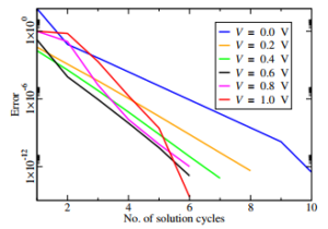
Figure 8: Same as Figure 7, using a 500-node grid.
7. Extension to Two Dimensions
It may be argued that a method for solving one-dimensional problems has a limited range of applicability. This is not so in the modeling of solid-state devices; in fact, when dealing with transport problems in structures like, e.g., carbon-nanotube transistors or nanowires, that are essentially cylindrical objects whose diameter is in the nanometer range, the restriction to the one-dimensional case is not too severe a constraint. In fact, for such devices the problem is typically separated by decoupling the longitudinal coordinate (the channel) from the transversal ones [11]; as no charge transport takes place in the directions transversal to the channel, separating the problem yields, for each transversal section, a system made of the Poisson and Schrodinger equations, which are further separated by¨ exploiting the radial symmetry of the device. As shown in Section 1, the one-dimensional Poisson and Schrodinger equations are solv-¨ able by NP. In turn, the transport along the channel is described by equations of the form discussed here, also amenable to the NP scheme.
Clearly the NP method would gain in flexibility from the exten-
sion to a non-uniform grid. This issue is outside the scope of this paper; the interested reader may refer to a method for extending NP to a variable stepsize, still in one dimension, based on the k-step Cowell method, which has been tested on the Schrodinger equation¨ (see [10] and references therein).
Another direction for evolving the NP scheme is the extension to more than one dimension using uniform grids of the tensor-product type. Such an extension, again applied to the case of the Schrodinger¨ equation, is described in [12]. It is of interest to ascertain whether the approach of [12] can be extended to the class of equations investigated here. To this purpose, one must first determine the multi-dimensional form of (7); the latter is obtained as follows,
The multi-dimensional form (22) shows that the equations describing charge transport in a semiconductor can be reduced to a single second-order equation of the elliptic type.
The notation becomes rather awkward even if one limits the extension to the two-dimensional case; taking a uniform, tensorproduct grid, and using the matrix notation of [12], namely,
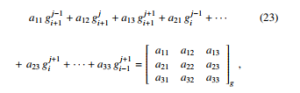
in which the lower indices of gij ,… refer to the x axis, and the upper ones refer to the y axis, the two-dimensional expansion yields an interpolation of the form
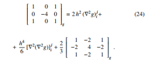
Calculating the Laplacian of both sides of (24), eliminating [∇2(∇2g)]ij after neglecting the derivatives of the 6th-order and, finally, replacing (∇2g)ij from (22) and defining the matrices.
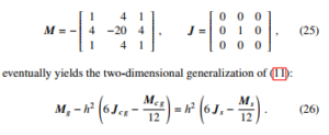
The result expressed by (26) shows that the approach of [12] can indeed be extended to the second-order equation of the general form; like in the one-dimensional case, no special assumption is necessary on the form of the discretized functions inside each elements or along its edges.
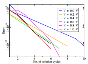
Figure 9: Same as Figures 7 and 8, using a 100-node grid.
8. Conclusions
It has been shown in this paper that the standard charge-transport
model in solid-state devices, made of the continuity and transport equations for the charge, can be given a form suitable for the application of the NP scheme, using a uniform grid in one or two
dimensions. With respect to the standard discretization schemes used in the analysis of semiconductor devices, the increase in the computational cost is modest; like in the case examined in [2], where the solution of the Schrodinger equation was takled, the NP¨ approach has provided a simple tool for improving the solution of
the equations.
In the field of semiconductor-device modeling, the results presented here are important from two points of view, already mentioned in Section 1: first, the NP approach, besides being able to significantly improve the solution, is applicable without excessive changes in the organization of the existing software; second, the drift-diffusion model on which NP has been tested is in fact the simplest level of description of solid-state devices; more sophisticated models exist, made of higher-order moments of the Boltzmann transport equation. On the other hand, such moments can always be grouped in pairs, each pair having the same structure: specifically, one equation of the pair is an even-order moment (order 2k, with k = 0,1,…) whose general form, with a suitable meaning of symbols, reads [9]
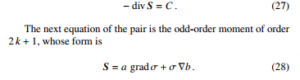
Comparing (27, 28) with (4) shows that all pairs of moments of the Boltzmann transport equation have the same structure. It follows that the method worked out in this paper applies to any order of transport models; also, considering that in the dynamic case the term C in (27) embeds the time derivative ∂σ/∂t, the method is applicable also in the dynamic operating mode of solid-state devices.
Appendix
Letting zi = z(xi), zi+1 = z(xi + h), zi−1 = z(xi − h), the series expansions around xi yield
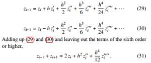
Multiplying (31) by h2/12, taking the second derivative of both sides, and leaving out again the sixth-order term,
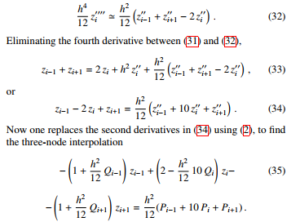
The method originates from [13] (cited, e.g., in [14]). It provides a three-point interpolation where the terms of the expansion that are left out are those of order six or larger; for this reason, it is superior to the standard finite-difference interpolation, although the computational load is comparable.
The method can be extended to higher orders. For instance, leaving out of the expansion the terms of order eight or larger, and using the short-hand notation −z00 = F(z, x), one finds the five-point interpolation

- N. Speciale, R. Brunetti and M. Rudan, “Extending the Numerov process to the semiconductor transport equations”, in 2019 IEEE International Conference on Simulation of Semiconductor Processes and Devices (SISPAD), Udine, Italy, 2019, 1–4, https://doi.org/10.1109/SISPAD.2019.8870513.
- F. Buscemi, E. Piccinini, R. Brunetti, and M. Rudan, “High-order solution scheme for transport in low-D devices”, in 2010 IEEE International Conference on Simulation of Semiconductor Processes and Devices (SISPAD), Yokohama, September 2014, 161–164. https://doi.org/10.1109/SISPAD.2014.6931588.
- International Roadmap for Devices and Systems (IRDSTM), 2020 Edition. https://irds.ieee.org/
- C. R. A. John Chelliah and R. Swaminathan, “Current trends in changing the channel in MOSFETs by III-V semiconducting nanostructures”, Nanotechnol. Rev., 6(6), 613–623, 2017. https://doi.org/10.1515/ntrev-2017-0155.
- O. Muscato, “Monte Carlo evaluation of the transport coefficients in an n+-n-n+ silicon diode”, COMPEL, 19(3), 812–828, 2000. https://doi.org/10.1108/03321640010334613.
- E. Piccinini, R. Brunetti, and M. Rudan, “Self-heating phase-change memory-array demonstrator for true random number generation”, IEEE Transactions on Electron Devices, 64(5), 2185–2192, 2017. http://dx.doi.org/10.1109/TED.2017.2673867.
- R. Brunetti, C. Jacoboni, E. Piccinini and M. Rudan, “Band transport and localised states in modelling the electric switching of chalcogenide materials”, Journal of Computational Electronics, 19(1), 128–136 (2020). https://doi.org/10.1007/s10825-019-01415-2
- D. L. Scharfetter and H. Gummel, “Large-signal analysis of a silicon Read diode oscillator”, IEEE Trans. Electron Dev., ED-16(1), 64–77, 1969. https://doi.org/10.1109/T-ED.1969.16566.
- M. Rudan, Physics of semiconductor devices. Springer, 2018. https://doi.org/10.1007/978-3-319-63154-7.
- J. Vigo-Aguiar and H. Ramos, “A variable-step Numerov method for the numer- ical solution of the Schro¨dinger equation”, Journal of Mathematical Chemistry, 37(3), 255–262, 2005. https://doi.org/10.1007/s10910-004-1467-3.
- M. Rudan, A. Gnudi, E. Gnani, S. Reggiani, and G. Baccarani, “Improving the accuracy of the Schro¨ dinger-Poisson solution in CNWs and CNTs,” in IEEE International Conference on Simulation of Semiconductor Processes and Devices (SISPAD), Bologna, September 2010, pp. 307–310. 10.1109/SIS- PAD.2010.5604497.
- T. Graen and H. Grubmu¨ ller, “NuSol–Numerical solver for the 3D station- ary nuclear Schro¨ dinger equation”, Computer Physics Communications, 198, 169–178, 2016. https://doi.org/10.1016/j.cpc.2015.08.023.
- B. Numerov. Publ. Obs. Central Astrophys., 2:188, 1933 (in Russian).
- P. C. Chow. Computer Solutions to the Schro¨dinger Equation. American J. of Physics, 40:730–734, May 1972. https://doi.org/10.1119/1.1986627