Wideband Active Switch for Electronic Warfare System Applications

Adv. Sci. Technol. Eng. Syst. J. 5(6), 1312–1321 (2020);
 DOI: 10.25046/aj0506156
Discrete component based ultra-wideband SPDT switch modelling, design and implementation challenges are reported in this article. The basic SPDT switch is planned to design using PIN diodes (bare die). Nonlinear parameters extraction steps of PIN diode from datasheets have been proposed in this article instead of using readymade nonlinear PIN diode models. Equalizers are designed as per requirement using discrete components and quarter wave transmission lines for different source and load impedances. Then all the designed components are integrated with a low noise amplifier (LNA). Extraction of PIN diodes’ nonlinear parameters are carried out using diode equations along with datasheet parameters. Layout has been implemented using microstrip and CPWG techniques. Quickly responding driver is designed using transistors and logic gates. CPWG based layout achieves better isolation compared to microstrip line-based layout at highest frequencies. Measured and simulated responses are tallied and they are matching together respectively except few exceptions. Measured responses also validates the well agreement between the proposed nonlinear diode modelling and equalizer design with different input and output impedances.
1. Introduction
Modern miniaturized systems require compact, light-weight and low cost components with high yield rate [1]. Excellent ultra wideband electronic warfare (EW) receiver like RWR (Radar Warning Receiver) system requires compact, lightweight and faster SPDT (single pole double through) switch which will be used to switch between BITE and RF ports. This active SPDT switch is basically used to control the RF port isolations while examining the whole Radar in BITE (built in test) mode. As the operating bandwidth of this module is very wide, microwave devices always struggle with uncertain gain gradients and ripples. Thus, excellent class wideband receiver of an RWR system are placed far away from its distributed antenna arrangement systems and connected through a lengthy cable. Thereby, it experiences enormous gain flatness problems particularly at higher frequencies due to excessive transmission line losses. To maintain the best flatness response, it is important to compensate the gain by flattening the gain response over the operating frequency band. It is commonly carried out by using passive equalizers. This article describes various design and development concerns/ problems etc. of wideband discrete components like SPDT switch, passive equalizers and the active SPDT switch. This article also shows a detailed method of nonlinear PIN diode model parameter extraction. Then a suitable PIN diode model is made using those extracted nonlinear parameters and has been used to design the PIN diode based SPDT switch. A suitable wideband LNA (Low Noise Amplifier) has also been introduced at the output path to compensate the loss of the SPDT switch. Prior art survey is carried out over design and development procedures of SPDT switches [2-9]. Allanic et. al. proposed a new passive SPDT design using silicon substrate in [2]. It is band limited to 5GHz with unequal losses in Tx and Rx ports. Additional amplifier is required to make it active SPDT. A high-power passive SPDT design is reported in [3]. Here also an additional LNA is required to make it active switch. Yang et. al. proposed an active SPST switch in [4]. This proposed SPST is band limited to 4GHz using InGaP/GaAs HBT process. This proposed switch consists of seven transistors. This SPST (single pole single through) switch is active in nature but does not cover wide frequency band. A high isolation active absorptive SPST is reported in [5]. It is band limited to 10GHz. Values of various parameters like, minimum gain, gain flatness, isolations and VSWR are -0.4dB, ±1.5dB, 35dB and 3.6:1 max respectively. Single chip SiGe BiCMOS based active SPDT and SPST designs are reported in [6] respectively. This design is also suffering from P1dB, gain, VSWR etc. Active wideband SPDT switch designs are proposed for V, D and Ku bands in [7–9] respectively. These proposed active SPDT switches are also suffering from gain, gain flatness, input output matching and isolations respectively. These reported designs are also lacking about P1dB and switching speed information except [9] (it provides only P1dB data). Present article uses a discrete LNA and integrates with PIN diode based SPDT switch. This article proposes nonlinear diode parameter extraction steps with an example using limited source of data (datasheet) and diode equations. Readymade nonlinear diode models have not been taken into consideration as vendor often do not extends support. Suitable diode models have been made using extracted nonlinear parameters and tuned up to 18GHz. Then those models have been used to design broadband switch. Equalizers are also designed separately with different input/output impedances to cope up with flatness issues. Only logic gates and discrete active components are used to design the driver where, NAND gate translates input logic to output logic control signals and transistor builds current over it. Active SPDT switch integrates separately designed SPDT, gain equalizers, LNA, attenuation pads, driver etc. Active SPDT switch was designed using microstrip lines initially, but isolation was not achieved 50dB. Then, co-planner waveguide (CPWG) approach is tried with one more extra shunt element for both the paths. This configuration achieves >50dB isolation at 18GHz. Switch isolation of microstrip line and CPWG based method is compared in the article. Switching speed of any switch is directly related to the signal throughput of the driver. Thus, how fast the driver acts switching speed will also be so faster. That is why it will be a combination of driver and switch’s performance respectively [10, 11].

Figure 1: Block diagram of ultra-wideband high speed active SPDT Switch consists of basic SPDT, equalizers, attenuator pads and LNA
This present work advances P1dB performances, power dissipation, better input/output matching and superior packaging with reduced weight respectively from the previous work reported in [1]. Figure 1 shows the block diagram of active SPDT switch where, BITE and RF-in are the two ports of the SPDT switch. Attenuator pad/equalizer are kept at the input of the switch for better matching [1]. It increases noise figure very little as compared to the previous situation where, active switch was absent. An appropriate LNA is integrated just at the output port of the discrete SPDT switch. Equalizers are used before and after LNA to keep flatness within the specifications. Measured and simulated responses are compared in this article and analyzed the probable cause of discrepancy. An appropriate reason is explained for this discrepancy and conclude about limitations of the nonlinear diode modelling. This article has been organized as follows. In Section 2, PIN diode parameters extraction, diode modelling, SPDT switch, equalizer and driver design are discussed. In Section 3, design implementation and experimentation are shown along with simulated results. In Section 4, fabricated switch is shown and the conclusions are given in Section 5.
2. Individual Components Design
This section explains about design steps of three important components design likely, nonlinear parameter extraction of PIN diodes, modelling and comparison with measured response (plotted in the datasheets), equalizer design and driver design respectively. The major work is involved in nonlinear parameter extraction of PIN diodes from datasheet and then prepare a suitable model out of it. Here this extraction steps will be explained in details. PIN diode modelling is carried out both for the diodes used in series and shunt branches of SPDT switch. Discrete component based equalizer design explained in the next and at last NAND gate based driver design also shown in details.
2.1. Nonlinear parameter extraction and PIN Diode Modelling
SPDT block of the active switch shown in Figure 1, has been designed using PIN diode bare dies. Simple nonlinear model of PIN diode is costly and most often component vendors’ do not support with exact nonlinear model parameter values in the datasheets. Thus it is necessary to make nonlinear model of PIN diode. It is possible to prepare nonlinear model of PIN diodes using data given in the datasheet [12]. Thus it has become designer’s capability to build an acceptable model for diodes using existing data in the datasheet. Extraction of all nonlinear model parameters are extremely difficult using limited source. Approximate (mere accurate) model is possible to make using these extracted parameters by fine tuning other model parameters and that can tackle the issue [12].

Figure 2: Classic diode model used to design circuit model of PIN diode
Adopting the above technique separate models have been prepared for shunt and series diodes respectively and compared with its measured responses. Figure 2 shows the basic diode model to be used to make equivalent PIN diode circuit model where, Cps, Cf, Cj, Lps, Rf, Rb, Rmax ID and Vjunc, are package parasitic capacitance, beam lead parasitic capacitance, junction capacitance, package parasitic inductance, minimum resistance when diode is in forward bias, variable i region resistance on PIN diode, maximum resistance, diode current and voltage across the junction respectively. Equation mentioned below (in 1) describes the current flowing through the diode where, Is, q, n, k, Tj and IRBD are, saturation current, electron charge, ideality factor, Boltzmann constant, temperature in kelvin and reverse breakdown current respectively [13].

where, VRBD and IRBDS are reverse breakdown voltage and saturation current respectively. Datasheet does not provide and package parasitic like, Cps, Cf and Lps and to describe the bonding pad paracitics. Thus, it is very difficult to extract all the model parameters from manufacturers’ data sheets, which only provide limited information. Fortunately, most of the critical parameters like, Is, Rf, Cj, τ, αc, δ etc. can be derived from the manufacturers’ data sheets where, τ, α and ζ are transition time, arbitrary constant and built in potential respectively [14]. Datasheet provides the I-R and C-V characteristics of diodes. Thus, all the above parameters can be extracted using these characteristic curves.


Figure 3: Comparison between modeled and measured DC C-V characteristic of HPND1084 PIN diode at 1MHz
where CD, CJ0, Fc and γ are capacitance due to the finite transit time (τ) through the i-region, depletion capacitance at Vjunc = 0, function of Vjunc, coefficient to divide the forward-bias, depletion capacitance into two regions and expressed by a 3rd order polynomial.

The resistance in the i-region is a function of the forward current. At high forward current level, Rb becomes close to zero. Thereby the minimum resistance becomes Rf. At reverse bias condition, Rb is almost infinite, therefore the maximum resistance is Rf +Rmax. The resistance at low and moderate forward current level is written in (6) [14].
![]()
Variable resistance can be found by putting in (9) in (8) considering β2=1, where Rm is the arbitrary RF resistance at current level Im.

![]()
Table 1 shows the extracted parameters considering HPND4018 PIN diode datasheet using (1) to (10). Here few parameters are directly taken from datasheet, like forward resistance, breakdown voltage, junction capacitance, transition time etc. Few other parameters have been finalized using curve
Table 1: The extracted model parameters for HPND4018 Diode

fitting technique to match the response with datasheet while simulation of model. PIN diode model simulation is performed in 2½D software taking parameters values from Table 1. Influence of bonding wires
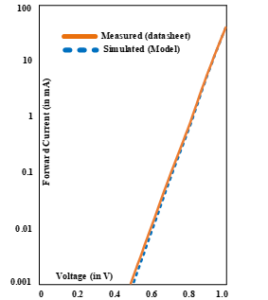
Figure 4: Comparison between modeled and measured DC I-V characteristic of HPND1084 PIN diode
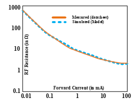
Figure 5: Comparison between modeled and measured RF resistance – Forward current at 100 MHz characteristic of HPND1084 PIN diode at 100 MHz
cannot be ignored while simulation. Thereby model is extracted including them. Tuning of the required model parameter values are carried out to match the model characteristics virtually similar

Figure 6: Simulated response of insertion loss, return loss and isolation characteristic of HPND1084 PIN diode
as compared to the datasheet. These models are purely made based on datasheet parameters and used for specific applications. Figure 3 shows the comparison between modeled and measured DC C-V characteristic of a HPND1084 PIN diode. Here modeled capacitance almost optimized as measured capacitance values. Figure 4 shows the comparison between modeled and measured DC I-V characteristic of the same PIN diode. Modeled current is showing a good agreement with measured current. Figure 5 shows the comparison between modeled and measured RF resistance characteristic. Here simulated resistance indicates that model parameters are optimized properly. Nonlinear model of MP6002 has also been carried out by following the above procedure. These two diode models are used for SPDT switch design, where, HPND1084 is used as series diode and MP6002 is used as shunt diode. Figure 6 shows the response of a modeled PIN diode (HPND1084) for 1– 20 GHz bandwidth. Maximum insertion loss is below 1dB at 18 GHz and it is well matched up to 18 GHz. Isolation is around 20dB at 18 GHz. The same loss characteristic is also calculated for shunt diode and kept ready for next level simulation. Here diode models are tuned several times to make it

Figure 7: Schematics of basic SPDT switch using PIN diodes
suitable and well matched with datasheet characteristics.
2.2. SPDT Switch Design using PIN Diodes
Simulated and verified nonlinear PIN diode models are used to design the SPDT switch where, HPND1084 is used in the series branch and MP6002 is used in the shunt branch. Schematic design of the switch is performed in 2½D software and shown in the Figure 7. Each branches of the switch having one series and three shunt diodes respectively. Here DC current return path is getting completed through inductor L and resistor R1 in the common path. Resistor R1 is used to limit the maximum current through the series diode. Bonding wires (2mil gold ribbon) have not been added in the schematics as it is already considered as parasitics in the diode modelling. The insertion loss (IL) and isolation (Iiso) parameters of the SPDT switch are estimated using (11) and (12) respectively. Here, Rfse, Rfsh, Z0, and XC are forward resistance of series and shunt diode, characteristic impedance, and reactive impedance respectively. Tendency of the simulated isolation response is fluctuating around middle of the frequency band which will be recompensed in final layout simulation [14].

where, , , here ρ and Ɛ are the resistivity of the I region and dielectric constant of the silicon.


Figure 8: Proposed layout diagram of basic SPDT switch using PIN diodes
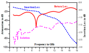
Figure 9: Simulated responses of proposed SPDT switch in 2½D software

Figure 10: Schematic diagram of single section equalizer
Reverse breakdown voltage, power handling, switching speed, capacitance, forward resistance, carrier lifetime, thermal resistance etc. have been kept in mind while selecting diodes. Final assembled layout of the proposed basic SPDT switch is shown in Figure 8. Here extra shunt diodes assembly option is kept in the layout so that fabrication iterations become less but, it has a disadvantage of higher insertion losses. This option will not affect at the overall performance as LNA is in the common path to compensate the extra losses. Initially, SPDT layout was carried out using microstrip lines and fabricated but, it was not meeting isolation specifications at higher frequencies (measured response is shown in the experimentation section). Thereby final layout of SPDT switch is made using CPWG lines in the first iteration. Figure 9 shows the simulated responses of the SPDT switch. Here insertion loss is about 2.8dB around 18GHz. Return loss is more than 20dB up to 14 GHz and it reduces to around 12 dB at 16–18GHz. Isolation is 50dB at 18 GHz. Now it is ready for next level integration with equalizer and LNA.
2.3. Equalizer Design
Equalizers are crucial parts for equalizing flatness of the module which, deteriorates with frequencies moving higher and higher. It is evident from Figure 9 that almost 2.5dB slope adjustment is must to flatten the switch response. Now there is an LNA in the common path that has its own gain slope (almost 2dB). Thus requirement specific equalizers are necessary in the various locations (common path as well as in the SPDT branches) to compensate all the loss/gain slopes. Figure 10 shows elementary schematic diagram of a single resonator based equalizer [1]. This equalizer is comprising of discrete thin film resistor and a resonator of λg/4 length at the highest frequency. Slope of the equalizer has been finalized after analyzing the integrated switch response in the system level simulations. Thereby case to case final component twigging will be performed as per need basis. The ultimate discrete component values can be finalized at the final level of simulations to maintain tiniest gain flatness (within ±0.5dB). Driving point impedance of the R-L-C network can be calculated using (13) where, R, L and C are the shunt resistance, inductance and capacitance respectively [15-17].

Final transfer characteristics of the equalizer containing n sections have been calculated by (14) where, ZL, is the load impedance and angular frequency respectively where, and f is the operating frequency.

Figure 11: Insertion loss response of equalizer for different resistor values.
![]()
Although (14) has been calculated for n number of sections but the actual number of equalizer sections may be changed/decided according to flatness characteristics at the final level of realization. Figure 11 shows insertion loss characteristics of passive equalizer varying numerous resistor (R) values where, upper and lower response curves are for lower and higher resistor values respectively. Now when it interacts with output impedance of SPDT switch as input impedance of it and input impedance of LNA as arbitrary load then its input and output port matching also changes respectively. Figure 12 shows the input and output return loss characteristics of the equalizer for numerous R values. Here source impedance is almost 50Ω but load impedance is the input impedance of the next stage thus, input and output return loss response is not symmetric. In the system simulations various resistor values have been tuned to achieve different slopes.

Figure 12: Input and output matching of equalizer for different resistor values
2.4. Driver Design

Figure 13: Schematic diagram and responses of switch driver circuit
A suitable driver is designed to generate the required control signals to operate the switch and LNA (supply sequencing) from external control signals. As it is discussed that the switching speed is a combination of driver and switch’s performance respectively [1]. Thereby design of appropriate driver is very crucial to achieve the best switching speed. Sequencing circuit is also required to feed supplies to the LNA. Here driver and sequencing circuit design is described in details. Logic gates, transistors, diodes etc. are used to design sequencing and driver circuit. External logic is passed through high throughput NAND gate and it passes through combination of transistors, zener diodes and resistor combinations to produce the output. Schematics level simulation of the driver is carried out using spice simulator tool. The design has also been verified by simulating the same circuit in 2½D simulator. The outcome of both the simulator tools are compared and they are very much satisfying. Figure 13 shows schematic diagram of a driver circuit comprises of logic gate (74LS00; dual-NAND gate) and zener diode (BGV90-C4V3) followed by transistors (current booster) and resistors in various combinations [1]. Simulated driver response is illustrated in the same Figure 13. In the Figure 13 the red color bit streams indicate the input control bits. The blue and violet color bit streams represent the output control–1 and control–2 bit streams respectively. These two output control bit streams are being used to alter the active switch RF and BITE paths respectively. It is also evident from the figure that, both the controls (control–1 and –2) are out of phase.

Figure 14: CPWG based schematic circuits staring from input port to output port of proposed SPDT switch for forward signal and Isolation path respectively
3. Active SPDT Switch Design
Active SPDT switch design has finally been performed by employing scattering parameter (.sNp) files of all the individually designed modules. RF system analysis depends upon the precise design of all the discrete modules. Hence it will meet all the necessary specifications across all the environmental conditions over an extensive frequency spectrum. Layout is made using CPWG lines as basic SPDT switch. This technique has been adopted to rectify isolation and insertion loss characteristics of the channel respectively. The final schematic level simulation is performed using 2½ D simulator tool. Schematic diagram of the active SPDT switch for forward and reverse (isolation) channel respectively are shown in Figure 14 [1]. Tapers used to interconnect two different impedance lines are not CPWG lines also shown in this Figure 14. Figure 15 shows the simulated blue color insertion gain curve and saffron color isolation curves of the proposed active SPDT switch. Here the overall gain about 2 dB is achieved with flatness within ±0.5dB. More than 50 dB isolation has successfully been met at 18 GHz which is very crucial parameter. Almost 95dB isolations are also met at the lower frequencies. Appropriate LNA (die), discrete component attenuators and readily available (designed) equalizers are used in the output track of the active SPDT to match the gain flatness. Simulated VSWR response is shown in Figure 16. Budget analysis has also been performed at -7 dBm input power level and at mid-band frequency (10 GHz) using 2½D software. Parameters like isolation, dynamic range, SFDR (spurious free dynamic range) and cascaded P1 dB had been the prime concern and they have attained 54.4 dB, 64 dB, 53.24 dB and 20 .7 dBm respectively. 3D EM simulation is carried out for the layout and mechanical channels respectively. It ensures any cavity resonance is present up to 18GHz or not. Ultrathin soft substrates have been used for fabrications. Driver and control circuit is made over FR4 material. The SP2T switch and driver/control circuits are mounted on opposite sides of the same housing respectively. Switch control, sequencing and other supply connections are taken from driver circuit board to switch side through small holes, keeping in mind the EMI/EMC effects. Appropriate mechanical channeling for RF circuits are important for achieving expected responses. Microwave channel dimensions are kept narrow enough to avoid higher mode resonance (excitations), as it disturbs characteristics of the module at higher frequencies. Carrier plate are made to ensure robust ground effects at higher frequencies and very good mechanical support to the PCBs. 0.4 mm kover and copper-molly sheets having nicely nickel plated with minimum impurities have been used to make carrier plates [19].

Figure 15: Gain and isolation simulation response of proposed SPDT switch in the transmission and isolation paths respectively

Figure 16: Input and output VSWR simulation response at input and one of the output ports of proposed SPDT switch
4. Experimentation
Active broadband SPDT switches have been developed using microstrip as well as CPWG lines respectively. Initially microstrip line based SP2T is developed and then CPWG line based switch due to noncompliance of isolation specification. The realized active SPDT switches are evaluated separately. Figure 17 shows the isolation responses of SPDT switch of microstrip line based approach. In this approach microwave channeling and air cavity sizes were not taken care precisely thereby output responses like isolation characteristics affected drastically. It is evident from the figure that isolation at 18 GHz is not meeting the requirement of 50dB. It is actually around 42dBc compared to gain plot. Gain plot of the microstrip line based SPDT is not shown as gain plot is identical to CPWG approach based SPDT. Comparison between measured and simulated responses of gain and isolation of CPWG approached based SPDT is shown in Figure 18 respectively. Here all measured and simulated responses are shown in firm and dotted lines respectively. Overall insertion gain met in this approached is 2.5dB except few frequencies. It is in good agreement with simulation responses. Each arm of this switch contains of sufficient gain equalizers to fit the gain flatness within ±0.4dB (maximum) over the entire spectrum at 27°C (Room Temperature; RT) as well as ±0.6 dB (maximum) across the wide temperature range -40°C to 71°C. Figure 18 also depicts the isolation response at RT which reached minimum 53dB (55dBc compared to gain response) in CPWG based approach.

Figure 17: Measured isolation responses between common port and port-1 and port-2 of the developed SPDT switch following microstrip line approach

Figure 18: Comparison between measured and simulated responses of gain and isolation of common port – port-1 and common port – port-2 of the developed SPDT switch following CPWG line approach
Any input port out of two input ports of the active SPDT switch can be accessed at any instant of time according to the external logic signal. This process achieves ON/OFF input output port isolation of 55dBc at the highest frequency and more than 60dBc across 1–15.5 GHz frequency. Tested isolation response is comparable with simulated response beyond 6GHz (6–18GHz). From 1–6GHz measured isolation is not matching to the simulation response due to more idealistic diode characteristics of the PIN diodes. Comparison between measured and simulated responses of VSWR of CPWG approached based SPDT is shown in Figure 19 respectively. The measured VSWR is 1.45:1 and 1.35:1 at the input and output ports respectively. Measured VSWR responses are in very good agreement of simulation responses. Better than 1.7:1 VSWR is measured across frequency band under ESS. About 50nS switching speed is measured with a very good rise and fall time characteristics.
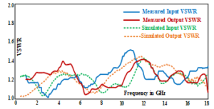
Figure 19: Comparison between measured and simulated responses of gain and isolation of common port – port-1 and common port – port-2 of the developed SPDT switch following CPWG line approach

Figure 20: Response of measured switching speed at the rising edge of the developed CPWG approach based active SPDT switch
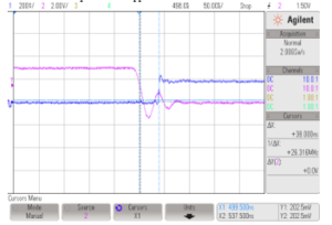
Figure 21: Response of measured switching speed at the trailing edge of the developed CPWG approach based active SPDT switch
Figure 20 and 21 describes the tested switching speed responses at rising and trailing edges against the input logic signal respectively. Here input switch control pulse is in ‘volt’ scale and detected output pulse in ‘millivolt’ scale although voltage scaling factor of input switch control and detected output pulses respectively is same (10:1). The detected output pulse will always be less than the input pulses as the input power level is fixed at -3dBm for switching speed measurement. This happens due to the absolute power level of the output pulses which is almost -1.5 – -1.0dBm (188–200mV) at 10GHz frequency and measured against a high value resistor (120Ω) is also shown in Figure 22 [18]. Thus final detected voltage after detector is very less compared to the external TTL signal. Achieved switch speed is 50nS including all RF and digital circuits. This module exhibits input P1 dB is >20 dB compared to prior work reported in [1]. This is achieved by replacing LNA with higher P1dB LNA, rectifying input/output port matching and twigging equalizer losses respectively. Developed active SPDT module also displays tremendous harmonics characteristics. Measured harmonics levels for 0dBm and 8dBm input signal for the active SPDT are 34dBc and 27dBc respectively. temperature cycling (TC) has been performed over -40° to +71° C and 3-axes random pre and post TC vibrations respectively.
Table 2: Measured data of SPDT switch after environmental stress screening carried out over 1–18 GHz Frequency band
| Sl. no | Parameters | Specifications | Min | Max |
| 1 | Gain | 2 ±2 dB | 1.8 dB | 2.3 dB |
| 2 | Isolation | 50 dB min | 54 dB | 73.1 dB |
| 3 | I/P VSWR | 2:1 (Max) | 1.2 | 1.3 |
| 4 | O/P VSWR | 2:1 (Max) | 1.2 | 1.5 |
| 5 | P1 dB (I/P) | >10 dBm | >20 dBm | |
| 6 | 2nd Harmonic | -25 dBc @ 0 dBm input -15 dBc @ 8 dBm input | -34 dBc -27 dBc | |
| 7 | Power handling | >1 watt | >1 W | |
| 8 | DC Power supply | -13V ( ±3%, -1%)/ 10 mA +13 ( ±1%, -3%)/ 50 mA | 1 mA 21 mA | |
| 9 | Switching Speed | 50 nS (Max) | 50.08 nS | 38 nS |
The outcomes of environmental stress screening (ESS) of the active switch are steady. The developed module is light weight and measured weight is less than 25 grams. Figure 22 shows the developed SPDT module and a classic arrangement for switching speed assessment [1]. It is clear form Figure 20 and 21, that, the switching speed is being measured between 50% of the external input control pulse and 90% or 10% of the final output pulse of the detector for rising and trailing edge respectively. Final achieved switching speed is nothing but the combination of active switch as well as doctor diode delay respectively. Thus the switching speed mentioned in the table 2 is more than the actual
| Table 3: Comparison between various parameter of recent works against present work
*switching speed has been measured including driver and others are without driver. |
switching speed of the active SPDT switch. Signal delay of the detector diode has been measured and it showed almost 5nS at highest frequency. Table 3 shows a comparative study of various parameters of recent works and the present work. Switching speed shown in the above table is different from other work as additional driver delay is added to the active SPDT switch of the present work. VSWR, gain flatness, isolation etc. are excellent compared to other work listed in the table. Another significant change has happened in the DC supply circuits. Earline simple line regulators were used to produce required supply from ±13V thus power consumptions were very high (almost 1.2W) in [1]. In the present work DC-DC converters are being used to generate required supplies for active components thereby power consumptions reduce drastically (almost 270mW). Thus, it can be established that the design goal has efficiently been reached as projected in the initial calculations.
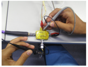
Figure 22: Measurement of switching speed by accessing input (TTL) signal to active SPDT switch and output detected pulse of the developed active SPDT switch module.
5. Conclusion
Ultra wideband active SPDT switch is designed using discrete modules like basic SPDT switch, equalizers, LNA, driver etc. Nonlinear PIN diode parameters extraction steps are shown in details using datasheet and diode equations. Nonlinear modelling is PIN diode is carried out and compared with measured responses (datasheet) for capacitance vs reverse voltage, forward current vs voltage and RF resistance vs forward current respectively. Extracted model parameters showed very good agreement with measured diode parameters. Separate modules are investigated, designed, assembled and evaluated separately. Passive equalizer with various component values are designed and finally most proper one has been selected for this active switch design. Final active switch parameters are plotted and tabulated against specification. Measured responses have been compared with simulated responses. Isolation characteristics of the developed module are not matching between simulation and measured responses from 1–5.7GHz. It happens due to limitations of PIN diode modelling. From the comparison of data, it is evident that the measured responses are in well in agreement with the simulated responses except few discrepancies. There are lots of future scopes regarding this work. LNA used in the present work has high gain which is not required as per present requirement. Thereby customized LNA can be designed to reduce power consumption further without affecting P1dB. This active SPDT switch can be compact by combining equalizers, PIN diodes, attenuators, driver and sequencing circuits as a multilayer (RF, DC and control circuit) single board solution as future work and further LNA can also be included within it using MMIC design solution as super compact light weight tiny chip.
Acknowledgment
Authors gratefully thank Mr. Manoj Jain, Head, Product Development and Innovation Centre and Mr. M.V. Rajasekhar, Director Research and Development, Bharat Electronics for their continuous inspiration to publish this work. Authors are also grateful to Microwave Super Component group, BEL for facilitating switch assembly, die bonding related processes and product design group for giving their support. They also thank all others who were involved directly or indirectly in this work.
- M. Sarkar, G. Anand, R. Sivakumar, “Light weight Active 1–18 GHz Ultra High Speed SPDT Switch for Radar Warning Receiver Systems,” IEEE /MTT-S International Microwave and RF Conference (IMaRC), 1–6, 2020, doi:10.1109/IMaRC2019.9116744
- R.D. Allanic, L. Berre, C. Quendo, D. Chouteau, V. Grimal, D. Valente, J. Billoue, “A novel 5-GHz SPDT Switch Using Semiconductor Distributed Doped Areas,” IEEE Microwave and Wireless Components Letters, 30(4), 421-424, 2020, doi:10.1109/LMWC.2020.2978644.
- “24–35 GHz GaAs MMIC High Isolation SPDT Reflective PIN Switch,” datasheet AP640R7–00, Alpha Industry Catalog.
- J.R. Yang, D. W. Kim, S. Hong “A 24 GHz Active SPST MMIC Switch with INGAP/GAAS HBTS,” Microwave and Optical Technology Letters, 50(8), 2155-2158, 2008, doi:10.1002/mop.23606
- I. Gresham, A. Jenkins, “A fast switching, high isolation absorptive SPST SiGe switch for 24 automotive applications”, 33rd European Microwave Conference, 3, 903–906, 2003, doi:10.1109/EUMA.2003.341108.
- T. M. Hancock, I. Gresham, G.M. Rebeiz, “A differential subnanosecond high-isolation absorptive active SiGe 24 GHz switch for UWB applications” Proc. IEEE Radio Frequency Integrated Circuits Symposium, 497–500, 2004, doi:10.1109/RFIC.2004.132065.
- A. Dyskin, S. Wagner, D. Ritter, I. Kallfass, “An Active 60–90 GHz Single Pole Double Throw Switch MMIC,” Journal of Millimeter Terahz Waves, 35, 412-417, 2014, doi:10.1007/s10762-014-0059-y.
- D. Muller, A. Tessmann, A. Leuther, T. Zwick, I. Kallfaaa., “Active Single Pole Double Throw Switches for D-Band Applications, IEEE/MTT-S International Microwave Symposium, 1–4, 2016, doi:10.1109/MWSYM.2016.7539969.
- M. Y. Chao, Z. T. Min, R. L. Chieh, K. Lin, Y. Chang, H. Wang, “Design and Analysis for a Miniature CMOS SPDT Switch Using Body-Floating Technique to Improve Power Performance,” IEEE Transactions on Microwave Theory and Techniques, 54(1), 31-39, 2006, doi:10.1109/TMTT.2005.860894.
- M. Sarkar, S. Jhariya, R. Sivakumar, “Correction of Nonunifirm Attenuation of Voltage Controlled Attenuator under Harsh Environment by Process Improvement” IEEE Transactions on Components, Packaging and Manufacturing Technology, 9(8), 1632-1642, 2019, doi:10.1109/TCPMT.2019.2929093.
- M. Sarkar, K. L. Santha, “ Designing of switch-limiter for Xband application in discrete components’ topology” 9th International Radar Symposium (IRSI-2013), 1–6, 2013, https\\:radarindia.com/ProceedingdArchive/IRSI-13/13-FP-139.pdf
- G. Antognetti, Massobrio, Semiconductor device modelling with SPICE, McGraw-Hill, 1993.
- S. M. Sze, Physics of Semiconductor Devices, John Wiley & Sons, 1981.
- Microsemi Corporation, The PIN Diode Circuit Designers’ Handbook, 1998.
- H. Wang, B. Yan, Z. Wang, R. Xu, “A Broadband Microwave Gain equalizer” PIER letters, 33, 63-72, 2012, doi:10.2528/PIERL12052309.
- M. Sarkar, V. Kumar, R. Sivakumar, R. Manjunath, N. S. Charulu, “Performance stabilization of steep gain gradient class ultra-wideband direct conversion IFM receiver of homodyning based systems” Int. Journal of Appl. Sci. 3(4), 27–31, 2017, issn: 2208-2182.
- T. F. Zhou, Y. Zhang, R. M. Xu, “Research on the millimeter wave gain equalizer,” IEEE International Conference on Microwave echnology & Computational Electromagnetics (ICMTCE), 180-182, 2011, Doi:10.1109/ICMTCE.2011.5915195.
- M. Sarkar, V. Kumar, R. Sivakumar, S. Jhariya, B. R. Raghu, K. S. Sudheesh, “Some investigations on Some Investigations on Direct Substrate-Attachment Process for Wideband Instantaneous Frequency Measurement Receiver Development” IEEE Transactions on Components, Packaging and Manufacturing Technology, 10(4), 704-716, 2020 doi:10.1109/TCPMT.2020.2966709.
- M. Sarkar, B. R. Raghu, K. S. Sudheesh, “Evaluation of Doubled-sided Substrate Attachment Technique for Round Shaped Large Metallic Housing under Airborne System Development,” IEEE 5th International Conference on Computing Communication and Automation (ICCCA), 191-194, 2020, doi:10.1109/ICCCA49541.2020.9250792.
No related articles were found.