Infrared Uplink Implementation for Software Defined Visible Light Communication Systems

Adv. Sci. Technol. Eng. Syst. J. 5(6), 127–132 (2020);
 DOI: 10.25046/aj050614
The main advantage of software-defined visible light communication (VLC) systems is that they allow us to reuse modulation, coding, synchronization and medium access techniques used in conventional radio systems. This article focuses on the implementation of an uplink alternative using an infrared (IR) light communication system. For this goal, analog front-ends are designed and implemented. Therefore, they convert a radio frequency signal into an optical signal. In addition, a Universal Software Radio Peripheral (USRP) is used as a software-defined radio platform. The obtained bit error rate is 5.33×10^(-5) using QPSK modulation with a bit rate of 4 Mbps at a distance of 160 cm between transmitter and receiver.
1. Introduction
This paper is an extension of work originally presented in 2019 IEEE Colombian Conference on Communications and Computing (COLCOM) [1]. This article aims to focus into the design process followed to implement analog front ends for the infrared (IR) communication uplink. On the other hand, an explanation is given about the blocks that make up the program to measure the bit error rate (BER) of the IR system. Finally, the signal-to-noise ratio (SNR) measurement is made and compared with the bit error rate (BER) obtained at different distances between transmitter and receiver.
Visible Light Communication (VLC) is currently being developed as a solution that enables the use of standard illumination light-emitting diodes (LEDs) to transmit data wirelessly. This type of communication is an alternative to mitigate the effects of saturation of the radioelectric spectrum in densely populated areas. Furthermore, it is known that the number of wireless devices connected to the internet is growing at an annual rate of 47% until 2021 [2]. This is mainly due to the greater access of terminal devices such as smartphones, tablets, laptops and recently to the deployment of the Internet of Things (IoT). For this reason, VLC is a technology that can serve as a complement of the currently deployed communication systems and provide access to the network. An important feature of VLC is that it can be used as a ubiquitous communication medium because LED lighting lamps are widely used in existing lighting infrastructure. On the other hand, VLC operates in the visible light band, which is not licensed and there is no electromagnetic interference generated by other communication equipment [3].
Information is sent and received through one or more LEDs on the transmitting side and a photodiode on the receiving side using a technique known as intensity modulation and direct detection (IM-DD) [4]. In such a way that the information that is sent produces variations in the level of illumination of the LED stage, these variations are imperceptible to the human eye. After that, the receiving photodiode converts the optical signal into an electrical signal for further processing.
In [5], the authors focused on the design and implementation of Analog Front-Ends, which would allow easy replication of the system through the use of low-cost components. The achieved bit rate was 20 kbps with a BER of using OOK modulation and Manchester encoding. In [6], a similar paper was done, but it did not specify the components of the designed interfaces, a BER of was measured at a bit rate of 2.5 Mbps and at a distance of 1.6 meters using BPSK modulation technique. In [7], an uplink based on infrared communication is proposed, the simulation result shows a value of 3.57 Gb / s using a transmitter with beam stearing and an angle diversity receiver. However, the experimental implementation stage of the system was not reached. In [8], it was possible to implement an infrared uplink by using an off-the-shelf receiver module (TSOP 1730) and the PPM modulation technique, however, the data transfer rate of the infrared link reaches up to 1200 bps. In [9], a surveillance camera is used as a receiver for an uplink based on infrared light. In [10], an IR link was implemented using a silicon integrated beam steering device, the achieved bit rate was 12.5 Gb/s and the bit error rate (BER) was less than .
This article shows the design and implementation process of Analog Front-Ends used on the transmitter and receiver side, achieving a bit rate of 4 Mbps and a BER of using QPSK modulation at a distance of 1.6 m. These interfaces have the advantage of being coupled to Software Defined Radio (SDR) systems, in such a way that the modulation, coding and synchronization of the data is carried out within a computer connected to a Universal Software Radio Peripheral (USRP). This allows for rapid prototyping and measurement of the IR communication system.
Section two presents the methodology used to carry out this work, section three delves into the design and implementation of Front-Ends, section 4 shows the results of the BER and SNR. Finally, section 5 shows the conclusions of this research work.
2. Methodology
Figure 1 shows the methodology followed to design and implement the Analog Front-Ends. First, an analysis of the communication system to be implemented is made. This analysis allows us to know all the elements that are required to make the VLC system work correctly. In addition, it is necessary to define the design parameters that allow the development of Analog Front-Ends. After that, the second procedure is Development of the Front-Ends. To carry out this task, it has been divided into two threads: design and implementation.

Figure 1: Methodology diagram
Finally, the last step is to carry out the corresponding measurements of the implemented communication system. To do this, a BER measurement is made as a function of the separation distance between transmitter and receiver. On the other hand, the measurement of the signal-to-noise ratio (SNR) is also carried out and a comparison is made with the previously measured BER.
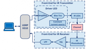
Figure 2: Block diagram of the IR communication system for BER measurement
3. Analysis of the Communication System
3.1. Block Diagram of the System
Figure 2 shows the block diagram of the IR communication system implemented for the purpose of making the BER measurement. This diagram is based on the research article previously made in [1] . It is observed that a laptop has a software stage where the modulation and synchronization of the information is carried out. After that, a USRP X300 is connected, which is a software-defined radio platform that allows to generate a modulated signal in the RF band. In this case, a central frequency of 5MHz has been used to carry out this test. Then, the signal goes to the transmitter front-end. This front-end is composed by an amplifier, a bias-tee, a constant current source and the IR LEDs. After that, the signal travels towards the receiver through the channel. In this case, the channel is the air in the indoor environment. On the other hand, the receiver front-end includes an IR photodiode, a transimpedance amplifier (TIA) and a low pass filter (LPF).
Table 1: Design Parameters for the IR link
| Parameter | Description |
| Application | Indoor |
| Coverage range | 1.6 m |
| Configuration | Direct LOS link |
| Bitrate | 4 Mbps |
| Modulation | QPSK / BPSK |
| Transmitter | LED Specification (each one)
– Radiant Intensity: 550 mW/sr – View angle: 10° – Wavelenght: 800 nm – 875 nm |
| Receiver | Photodiode specifications:
– Code: SFH 203 FA – Spectral response: 800 nm – 1100 nm – Sensitive area: 1 |
| OP-AMPs | LT6268-10 and LT6268 with dual supply ±2.5 |
3.2. Design Parameters
The design parameters of the electronic circuits for the transmitter and receiver analog interfaces are shown in Table 1. It is observed that the configuration used in this paper requires a line of sight (LOS), this is due to the fact that the angle of view of the LEDs arrangement is 10°. Which allows maximum energy transfer in only one direction. In this way, the use of an optical lens that amplifies the optical signal at the receiver is avoided. In addition to this, the other parameters taken into account to implement this communication system can be read.
4. Development of Front-Ends
Front-ends are developed based on the design parameters mentioned in the previous section. First, the design of the front-ends is done. After that, the physical implementation of them is made.
4.1. Transmitter Design
The transmitter front-end is composed by four blocks. The first block is an amplifier that must take the signal from the USRP and feed a LED array. The second block is a bias-tee that superimposes the RF signal coming from the amplifier on a constant current level coming from the third block called “Constant current source”. The three previous blocks make up the LED driver. Finally, the last block is an array of LEDs, it is composed of eight high-power LEDs placed in series, which produce an optical signal that will travel through free space until it reaches the receiver front-end.
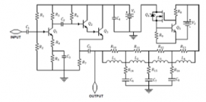
Figure 3: Schematic circuit of the Transmitter Front-end
Figure 3 shows the schematic circuit of the transmitter front-end, it can be seen that it includes a common emitter amplifier, that includes the transistor . After that, the circuit is followed by a Darlington amplifier, which is made of the transistors and . The common emitter amplifier was designed following the procedure described in [11]. The design equations are as follows:

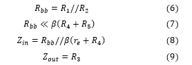
From (1) the base current is obtained from the value of the collector current, which in this case is 10 mA, in addition β has a value of 95. In (2) and (4), has a value of 12 V. The values of the resistors , and are calculated from (4) and (5). On the other hand, (6) and (7) allow the calculation of and . Next, (8) and (9) allow us to know the input and output impedances. Finally, a Darlington amplifier is inserted to reduce the output impedance and increase the output power.
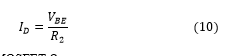
In Figure 3, is a MOSFET that provides a constant current source whose value is defined by (10). In this case, 140 mA was chosen as the value because it allows the LEDs to keep turned on.
: drain current of MOSFET
: Base-Emitter Saturation Voltage of Transistor
LED’s must be turned on to modulate their light intensity without turning them off. For this purpose, it is necessary to superimpose the AC signal coming from the amplifier with the DC level coming from the constant current source. The bias-tee is in charge of this task. Finally, this LED driver is connected to an array of eight LEDs in series. In this way, the Front-end transmitter has been designed.
4.2. Receiver Design
Figure 4 shows the schematic circuit of the receiver front-end, which is composed of a photodiode, a transimpedance amplifier and a low-pass filter. The photodiode makes it possible to transform an optical signal into an electrical one. In this project, the SFH 203 FA photodiode is used, which has a switching time of 5 ns, it is inversely polarized with a voltage of 12 V. Furthermore, and constitute a low-pass RC filter in order to eliminate noise from source .
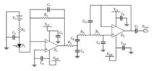
Figure 4: Schematic circuit of the Receiver Front-end
The current at the output of the photodiode enters a transimpedance amplifier. The gain of the transimpedance amplifier is equal to the feedback resistance . After a voltage is obtained at the output of the transimpedance amplifier (TIA), the signal passes through a two-stage low-pass filter. The first stage is made up of an RC filter composed of and and whose cutoff frequency can be calculated using (11). After that, the coupling capacitor is connected, this capacitor allows only the alternating component of the signal to pass. In this way, the voltage produced by the ambient light is minimized. Finally, a Chebyshev low-pass filter is responsible for eliminating high-frequency noise and adapting the output impedance for connection to the USRP equipment. The design of this filter was done following the procedure described in [12], the calculations were made using (12), (13), (14) and (15).
4.3. Implementation of Front-ends
The transmitter front-end was implemented as shown in Figure 5. The physical implementation of this circuit can be shown on two single printed circuit boards (PCB). Figure 5.a shows the LED driver. On the other hand, Figure 5.b is the IR-LED array. The reason why the LED array is not included in the same PCB is because it allows to do further tests with different LED configurations. In this way, it is avoided to build new front-ends in order to speed up the tests and improve the transmitting analog interface. Both circuits are connected by a coaxial cable in the experimental setup.
Figure 6 shows the physical circuit of the receiver front-end for the IR uplink. It is observed that the output connection is made through a female SMA connector, to which an RG58 coaxial cable is connected.

Figure 5: Physical implementation of the transmitter Front-end.
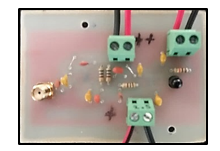
Figure 6: Physical implementation of the receiver Front-end
5. Measurements
Once the Front-ends have been implemented, the Bit Error Rate (BER) measurement is performed. To do this, it is necessary to establish the experimental setup shown in Figure 7. This setup is based on the block diagram described in the third section of this paper. The connection between the laptop and the USRP is made through a gigabit ethernet cable. The connections between the USRP and the front-ends are made through RG58 coaxial cable.
To carry out the BER measurement, the program shown in Figure 8 is used. This program was developed in GNU Radio from the information available in [6], with the difference that now QPSK modulation and the rate are used. sampling rate is changed to 4 MS/s.

Figure 7: Experimental setup for BER measurement
The explanation of the blocks that make up this program is as follows:
- The “PRBS Source B” block is responsible for generating a random sequence of bits, which is repeated indefinitely.
- “Preamble Insert” is a block that inserts a bit preamble, which is used to indicate the moment at which the BER measurement starts.
- “Bit to Symbol Mapper” takes care of QPSK modulation. In addition, it assigns values to the transmitted symbols. This can also be changed for using BPSK modulation.
- “Root Raiced Cosine Filter” is a block that is used in transmission and reception to minimize intersymbolic interference.
- “Costas Loop” is responsible for the frequency recovery of the carrier signal.
- “Clock Recovery MM” has the function of time synchronization.
- Subsequently, the “Decode using Preamble Synch” block takes care of the demodulation and detection of the preamble to start the BER measurement.
- The “Binary Slicer” block transforms the demodulated signal into bits. These bits can have two values 0 or 1.
- Finally, the “PRBS Sink B” block is in charge of comparing the received bits with the original sequence and showing the bit error rate (BER).
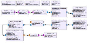
Figure 8: Program in GNU Radio for BER measurement using QPSK modulation
Figure 9 shows the results obtained from the BER measurement as a function of the separation distance between transmitter and receiver. The red graph indicates the BER measured using QPSK modulation at a bit rate of 4 Mbps. A BER of was obtained at a distance of 160 cm between transmitter and receiver. The blue graph shows the BER obtained using BPSK modulation, which has a value of at a distance of 160 cm and the bit rate is reduced to 2 Mbps.
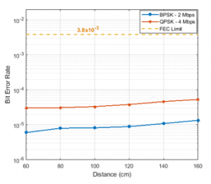
Figure 9: BER with respect to distance
Finally, signal-to-noise ratio (SNR) is measured at different distances between the transmitter and receiver using BPSK modulation. From the obtained data, it has been possible to make the graph of Figure 10, in which the BER is observed as a function of the SNR. With a SNR of 36.2 dB, a BER of was measured. In the other hand, with a SNR of 46.4 dB, a BER of was obtained. It can be seen that, if the SNR increases, a lower BER is measured. In this way, having an SNR greater than 45 dB, the BER seems to converge, however this is due to the fact that a finite number of packets were sent. Therefore, it is convenient to have the least amount of noise in the system or, failing that, to increase the power of the transmitted signal.

Figure 10: Measured BER vs SNR
6. Conclusions
- A bit error rate of has been measured when transmitting at a bit rate of 4 Mbps using QPSK modulation at a distance of 160 cm between transmitter and receiver for an infrared light communication system.
- Signal to noise ratio decreases when the distance between transmitter and receiver is greater. In turn, the bit error rate increases as there is a lower signal-to-noise ratio.
- The transmitter front-end provides a constant current level of 140 mA, this keeps the LED stage turned on, while at the same it is modulated the intensity of the optical signal.
- The receiver front-end is composed by a transimpedance amplifier and a two-stage low-pass filter. The output voltage does not exceed 2 Vpp, which is the input limit for a USRP X300.
- A software program was developed in GNU Radio to measure the bit error rate of the infrared communication link. The used sampling rate is 4 MS/s and the central operating frequency is 5 MHz.
- Front-ends have been designed and implemented for infrared light communication that can be used in Software Defined Radio systems as an alternative for VLC uplink. Taking into account the requirements of this type of links.
- The main advantage of this system is that, as it is based on software defined radio, the modulation, coding and synchronization stages are implemented within a personal computer. Therefore, to implement it, it is necessary to use analog front-ends that allow the conversion of RF signals to optical signals.
- The main disadvantage is that the bit rate is limited by the capacity of the computer processor where the transmission and reception programs are executed, it was necessary to carry out tests with different personal computers and the one with the best performance was chosen.
Conflict of Interest
The author declares no conflict of interest.
Acknowledgment
The author thanks to the National University of San Agustin of Arequipa for providing access to the laboratories to carry out the tests of this paper. On the other hand, the author also thanks to professors Alex Cartagena Gordillo, Pablo Lizardo Pari Pinto and Ruben Matheos Herrera.
- O.R. Banda Sayco, A.C. Gordillo, “Development of an IR system as an alternative for VLC uplink,” in 2019 IEEE Colombian Conference on Communications and Computing (COLCOM), IEEE: 1–5, 2019, doi:10.1109/ColComCon.2019.8809131.
- M. Uysal, “Visible Light Communications: From Theory to Industrial Standardization,” in Optical Fiber Communication Conference (OFC) 2019, OSA, Washington, D.C.: Th3I.4, 2019, doi:10.1364/OFC.2019.Th3I.4.
- Z. Wang, Q. Wang, W. Huang, Z. Xu, Visible Light Communications Modulation and Signal Processing, 2017.
- P. Kamsula, Desing and implementation of a bi-directional visible light communication testbed, University of Oulu, 2015.
- M. Basha, M.J.N. Sibley, P.J. Mather, A. Makama, “Design and Implementation of a Tuned Analog Front-End for Extending VLC Transmission Range,” in 2018 International Conference on Computing, Electronics & Communications Engineering (iCCECE), IEEE: 173–177, 2018, doi:10.1109/iCCECOME.2018.8658815.
- O.R.B. Sayco, A.C. Gordillo, “Design and Implementation for a USRP – Based Visible Light Communications Transceiver,” in 2019 UNSA International Symposium on Communications (UNSA ISCOMM), IEEE: 1–5, 2019, doi:10.1109/UNSAISC.2019.8712826.
- O.Z. Alsulami, M.T. Alresheedi, J.M.H. Elmirghani, “Infrared Uplink Design for Visible Light Communication (VLC) Systems with Beam Steering,” in 2019 IEEE International Conference on Computational Science and Engineering (CSE) and IEEE International Conference on Embedded and Ubiquitous Computing (EUC), IEEE: 57–60, 2019, doi:10.1109/CSE/EUC.2019.00020.
- T. Adiono, A. Pradana, R.V.W. Putra, W.A. Cahyadi, Y.H. Chung, “Physical layer design with analog front end for bidirectional DCO-OFDM visible light communications,” Optik, 138, 103–118, 2017, doi:10.1016/j.ijleo.2017.03.046.
- T.C. Bui, S. Kiravittaya, “Demonstration of using camera communication based infrared LED for uplink in indoor visible light communication,” in 2016 IEEE 6th International Conference on Communications and Electronics, IEEE ICCE 2016, 2016, doi:10.1109/CCE.2016.7562615.
- K. Wang, Z. Yuan, E. Wong, K. Alameh, H. Li, K. Sithamparanathan, E. Skafidas, “Experimental demonstration of indoor infrared optical wireless communications with a silicon photonic integrated circuit,” Journal of Lightwave Technology, 2019, doi:10.1109/JLT.2018.2889252.
- Hunter College – City University of New York, “15. Transistor Amplifier Design and Measurement,” [Online]. Available: http://www.hunter.cuny.edu/physics/courses/physics222/repository/files/pdf/ElectronicsLab15.pdf
- T. Kugelstadt, Active Filter Design Techniques, Elsevier: 365–438, 2009, doi:10.1016/B978-1-85617-505-0.00020-X.