Design and Implementation of DFT Technique to Verify LBIST at RTL Level

Adv. Sci. Technol. Eng. Syst. J. 5(6), 937–943 (2020);
 DOI: 10.25046/aj0506111
According to IEC 61805 and ISO 26262 standards requirement inclusion of LBIST (Logic Built in Self-Test) became mandatory to achieve safety critical application such as automotive field. In such systems, once device is switched ON LBIST (Logic Built in Self-Test) is activated and testing of digital logic is performed. After safety subsystem says that the LBIST passed, the SoC (System on Chip) moves into the functional mode otherwise, the SoC moves into a safe state. In this entire start-up sequence the LBIST interacts extensively with the safety sub-system of the SoC. Startup sequence remains un-verified at RTL (Register-Transfer Level) leading to painful ECOs (Engineering Change Orders) and post Silicon issues in some cases. LBIST verification can only run if scan chains are present in design which is not the case at RTL. The paper describes design of a Design-for-Testability (DFT) technique to enable LBIST based system verification with different test approaches at RTL which eliminates the possibility of ECOs by catching most of the issues at RTL level. Simulation results are demonstrating the feasibility of the approach with emphasizing the benefits obtained on significant computational modules.
1. Introduction
LBIST became alternative approach for ATPG (Automatic Test Pattern Generation) due to increased complexity and test cost requirement for functional blocks [1]-[3]. Electronic component general safety-critical applications [4] are referenced in IEC 61805 [5] and Automotive Safety Integrity Level (ASIL) for automotive domain is referenced in ISO 26262 standard [6].
Latent faults (LFs) detection for automotive systems using power on self-test (POST) based on logic built in self-test (LBIST) is executed during engine start -up to test safety – critical devices before staring any functional operations [7]. POST is having limited test application time in automotive systems [8]. Getting required LF coverage (>90%) within less test application time is primary requirement [9].
the pass/fail comparison of the unit [10], [11]. PRPG (Pseudo Random Pattern Generator) is used for generating input stimulus for the design, and MISR (Multiple Input Signature Register) to capture the compact the response. Test patterns which is supplied to internal scan chains are output of PRPG block and response is the input to the MISR compaction. Signature is the compacted response for that cycle of operation [12], [13]. The LBIST implementation is as shown in Figure 1.
LBIST is based on ‘scan’ methodology to test digital logic [14], this suffers from limitation – The design cycle will be delayed by the time the netlist is ready with Scan insertion, X-bounding [15] and Test-point insertion done [16] to perform LBIST verification. Performing LBIST patterns gate-level simulations early in the design cycle will take weeks to complete since execution is performed in series and are large number [17].
In this paper, we propose an innovative strategy for the in-field testing of automotive devices. Methodology to perform parallel verification of sub-modules of System on Chip (SoC) is described. Section 2 describes proposed design methodology to per-form Logic BIST verification at RTL level with dummy netlist. Section 3 describes implementation details such as scan chain insertion steps, dumpy netlist creation and direct mode entry. Simulation results with debugging analysis details are discussed in section 4 and in section 5 conclusion of the work is described.
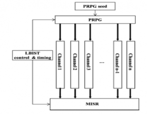
Figure 1: Standard LBIST Implementation
2. Proposed Design Methodology
Logic Built-In Self-Test (LBIST) is implemented by several LBIST controllers which operate independently on different partitions of the device as shown in Figure 2. This is needed to fulfil safety requirements about the independence and diversity of replicated IP, helps in physical flow and helps to avoid exceeding power limits. For applying traditional external scan patterns, LBIST controllers are put into trans-parent mode. Typically scan chains used for LBIST are shorter than scan chains used for compressed ATPG (Automatic Test Pattern Generation). Therefore, in LBIST transparency mode, the short LBIST chains are concatenated during to longer pro-duction scan chains which then are connected to the EDT (Embedded Deterministic Test) scan compression IP.
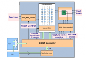
Figure 2: LBIST Architecture
LBIST controller IP itself will become part of the scan chains used for external scan patterns. Certain registers may not change value during LBIST operation but should be part of regular ATPG scan. These registers are put into one or more separate scan chains which are not shifted during LBIST. During LBIST their values are not influenced by shifting. These special scan chains are only used for ATPG. These registers will be identified during implementation. Each of the LBIST controllers is connected independently to the STCU (Self-Test Control Unit). The STCU can either start all LBIST controllers at the same time in parallel or in a sequence defined by the STCU. Only for debug reasons it is possible to access and operate each LBIST controller separately. This is done via JTAG (Joint Test Action Group) and a path through TCU (Test Control Unit) to the selected LBIST controller.
2.1. LBIST Partitioning
According to the safety concept eight LBIST partitions are implemented. They are numbered A0, A1, B0, B1, C0, C1, P0, P1. Each LBIST partition is contained in a separate LBIST island or lake as shown in Table 1. List of blocks where LBIST implementation is exempted:
- JTAG Controller
- TCU
- IO_top level ((Input-Output) / Pad ring
- PMU (Power Management Unit)/ PMU-Controller
- STCU
- PLL (Phase Locked Loop)
- XOSC (Oscillator)
Table 1: Characteristic data of LBIST partitions
| Characteristics | |||||
| Partition | Size | LBIST chains | PRPG
size |
Clock domains | Chain overhead |
| A0 | 77K | 1600 | 46 | System,
tck |
10% |
| A1 | 60K | 1100 | 36 | System,
tck |
10% |
| B0 | 24K | 500 | 24 | System,
tck |
10% |
| B1 | 60K | 1100 | 36 | System,
tck |
10% |
| C0 | 45K | 1000 | 34 | System,
tck |
10% |
| C1 | 60K | 1100 | 36 | System,
tck |
10% |
| P0 | 26K | 600 | 26 | System,
tck |
10% |
| P1 | 60K | 1100 | 36 | System,
tck |
10% |
2.2. LBIST Integration
The design is split into several LBIST islands, where each LBIST island contains the actual LBIST partition, i.e. the logic to be covered by LBIST, a dedicated LBIST controller, dedicated clock and reset control blocks as shown in Figure 3. LBIST Controller:
Essential features of the LBIST controller IP used are:
- External clock control.
- Serial and parallel interface (to simplify communication, both functional and test/debug).
- Neg-edge lockup registers after PRPG and before MISR (to simplify LBIST scan chain timing)
With the introduction of lockup registers after PRPG and before MISR all LBIST scan chains must begin and end with a pos-edge flop. With this architecture all LBIST clock domains with less than half a cycle clock skew can be handled safely.

Figure 3: Basic Blocks per Physical Partition
LBIST Controller Hierarchy: The controller needs to be generated with the following parameters:
set rtl hierarchy -Clk_mux Out -external_clk_enables
set lbist Controller -programmable_shift_rate ON
set shift_rate Divisor 8
This generates the LBIST controller IP in a hierarchy. The LBIST clock controller is entirely based on clock enable rather than the clocks generated by the LBIST IP in order not to generate a new clock path. Figure 4 gives an overview of the generated Controller IP and its hierarchy.
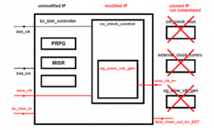
Figure 4: LBIST Controller IP Hierarchy
2.3. LBIST Controller Clocks
The LBIST controller operates on three different clocks, the LBIST engine clocks, bist_clk, and slow_clk, as well as the STCU communication clock bist_tck. The LBIST engine clocks bist_clk and slow_clk must fulfill the following requirements:
- The clock source for ‘bist_clk’ and ‘slow_clk’ must be identical.
- The clock source for ‘bist_clk’ and ‘slow_clk’ must be the fastest clock used inside the LBIST partition.
- The clock source for ‘bist_clk’ and ‘slow_clk’ must be the clock with the highest clock insertion delay used inside the LBIST partition.
2.4. LBIST Interface Dummy
The LBIST interface dummy propagates a standard LBIST interface into the LBIST partition, to ensure, that all relevant signals are present and preserved through synthesis and scan insertion. The LBIST interface dummy combines the following interfaces / features:
- LBIST controller IP interface
- LBIST clock interface
- LBIST clock gating control (‘ipt_cg_bypass’ and ‘ipt_se_gatedclk’)
- Test points that can be connected by the physical team to improve coverage if required
- Production Scan: Launch-Off-Shift (LOS) per clock domain and blocking of LBIST control signals for at-speed scan.
The LBIST interface dummy is protected during synthesis because connections to the module are created during scan chain stitching and automatic clock gate insertion only.
2.5. LBIST Interface Dummy
For direct execution of LBIST, the optional parallel interface of Mentor’s LBIST controller is used. It provides the following interface signals:
- bist_run_input- triggers LBIST run
- bist_done – flags a finished LBIST run
- misr_value – vector output providing parallel read access to MISR value
Debug and diagnosis require access to LBIST control registers. It is done through LBIST’s serial interface. Writing and reading control registers happens in a JTAG-like serial mode. The LBIST serial debug interface is used by the STCU to con-figure LBIST run parameter, such as pattern count. Full debug and diagnosis are performed through the TCU only. The interface is based on a JTAG-like protocol with shift- and update-DR states. Both TCU and STCU share the interface to the LBIST controller IP, where the muxing between TCU and STCU is performed inside the STCU controlled by ‘tcu_lbist_direct_ctrl’. The actual TCU access is performed though the TCU external TDR mechanism based on the register selection through the LBIST TDR (LTDR). Expected LBIST signatures are kept in the Non-Volatile Memory (NVM). Through STCU programming the required signature is fetched from the NVM for comparison.
2.6. LBIST Clock and Reset Control
LBIST Clock Control: All LBIST clocks are controlled through the Magic Carpet Clock Gating Logic (MC_CGL) associated with each LBIST partition. The clock control by the MC_CGL is purely based on clock enables rather than the clocks generated by the LBIST IP. Figure 3 shows the modules relevant for LBIST clock control for one LBIST partition ‘C0’.
The LBIST controller, as well as the blocks lbist_clock_control, lbist_cgl_control, and cgl_lake exist local to all eight LBIST partitions. The LBIST controller with its modified co_clock_control block is connected to the main lbist_clock_control module, that combines the shift and capture enable signals. The lbist_cgl_control block switches between the clock enables generated by the TCU and by the LBIST controllers depending on the mode setting. The clock gate inside the MC_CGL will generate the slow bist clock based on the enable provided by the LBIST IP. The LBIST clock control will provide punch out clocks, not 50% duty cycle clocks.
Slow Clock Generation: The LBIST slow clock (‘slow_clock’) is a punch out clock divided down from bist_clk (== fast_clk) using a programmable clock divider inside the ‘sg_slow_clock_gen’. It is used to control several key LBIST functions, such as PRPG, MISR, pattern counter etc. The same slow clock divider is used to program the shift clock frequency. The default divider ratio of the ‘sg_slow_clk_gen’ module is set to 8 but can be reprogrammed via the LBIST control registers.
LBIST Reset Control: To control all resets within the LBIST partition, all resets must be routed through the LBIST reset control block. The block allows reset control for LBIST, while the system resets are not gated. This is to make sure, that a system reset is not blocked during device startup.
LBIST reset requirements are:
- All asynchronous resets of an LBIST partition must be routed through the LBIST reset control block.
- All functional resets must be in off state during LBIST execution.
- No LBIST partition output to MC_RGM/MC_RSL must have an influence on self-test / LBIST execution.
The original reset control logic provided by the LBIST controller IP is an active-high reset (clock) signal multiplexed into the functional reset path. With the non-blocking reset control, where the functional reset is not blocked by LBIST a new reset control is introduced replacing the original one. To pre-vent reset glitches from propagating into the LBIST partition in scan mode, the LBIST reset control must be bypassed by a scan mode reset. The non- blocking reset control dictates, that all functional resets are off during LBIST execution, otherwise the LBIST MISR becomes invalid.
2.7. Making the LBIST Partitions LBIST Ready
The interface of the LBIST partitions need special attention to ensure that there is no X poisoning into the LBIST partition. All critical signals causing problems in the standard X-bounding flow will be X-bound in RTL. Mentor Testkompress fault simulation is used to identify missing X-bounds. The decision on whether an input is to be X-bounded is taken based on the partition input signal categories shown in Table 2.
The X-bounds inserted in RTL will instantiate a MUX controlled by lbist_en from the LBIST controller IP. Whenever possible the partition outputs are used as inputs to the MUX. This increases coverage as it provides toggling and not constant inputs to the MUXes, while at the same time adding observability to the partition outputs.
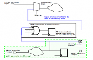
Figure 5: X-bounding to avoid multi-cycle path generation
Figure 5 shows a concept used to avoid multi-cycle path generation on known critical input – output combination. The LBIST interface dummy module will include several XOR gate FF combinations as shown below. The RTL X-bounding flow uses and connects these structures. In a later stage the automatic RTL x-bounding flow might also include instantiation of these structures instead of using predefined ones.
Table 2: LBIST partition input categories
| Category | LBIST Control | Bound |
| Reset input | Via LBIST reset control | No |
| Clock input | Via LBIST clock control | No |
| Clock gate control | Via LBIST interface dummy | No |
| Common Digital Input | Yes | |
| Selected Tied Digital Input | Yes | |
| Unconnected Digital Input | None required | No |
| Digital Input from TCU – no influence on LBIST | yes | |
| Digital Input from TCU – influence on LBIST | Constant from TCU | No |
| Bidirectional | NA | No |
| Analog/Special Nets | All hard IP in LBIST mode | No |
| LBIST Controls | From LBIST control IP | No |
3. Implementation Details
LBIST scan chain insertion and concatenation to top level LBIST chains including lockup-FF insertion followed these basic steps in the DFT and physical flow.
- DFT flow – Generated EDT controllers everything pos-edge based w/o lockup-FFs
- DFT flow – Generated LBIST Controller and connected internal LBIST chains at the BIST controller to form ATPG scan chains. Modified LBIST controller to provide ATPG chain outputs with LBIST controller interface. Connecting ATPG chain inputs and outputs of LBIST controller to EDT controllers using IPXACT flow. (Assigned fixed value to EDT controller pins for remaining chains outside LBIST to protect them in synthesis)
- Physical flow -One step scan insertion: Building LBIST chains, connecting them to the LBIST controller. Building ATPG chains for logic outside LBIST, connect-ed them to the EDT controller using the pins with fixed value assigned by IPXACT.
- Physical flow – Post processing step to insert lockup FFs, including required lockup-FFs in concatenated LBIST chains.
- Checked for missing lockup-FFs on
- change of clock name or clock polarity in scan cell report – DFT flow
- clock hierarchy change – Physical flow
Figure 6 depicts concatenation of four LBIST scan chains to form one production chain with input and output available at the LBIST controller boundary for hook up to the EDT controller. Also shows where lockup FFs are placed by the physical flow.
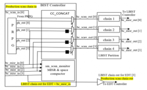
Figure 6: LBIST chain concatenation and lockup latch insertion
3.1. LBIST Dummy Netlist Integration at RTL
Integrating a dummy netlist in the design at RTL level with the same number of scan chains, scan clocks and scan resets is done. This dummy netlist should only be visible to the verification environment, in the LBIST testcases expect the MISR calculated for the dummy netlist.
Flow: Generate a dummy netlist (with scan chains) à Generate the MISR value for the same dummy netlist àIntegrate this dummy netlist into the actual design RTL à run the testcases for verifying the complete start-up sequence. Details of each step are described below:
Step1: Generate a dummy netlist using “skeleton design creation”.
create_skeleton_design -o lbist_for_verif -i skeleton_design.txt
Step2: Generate MISR for dummy netlist by doing fault simulation using LBIST Architect
lbistarchitect -fault_simulation \
lbist_for_verif.v -verilog \
-lib skeleton.fslib -nogui \
-dofile lbist_for_verif.dofile
Step3: Integrate the dummy netlist into the lbist partition using “ifdef”
Step4: Perform RTL simulations for LBIST based start-up sequence using the com-pilation argument:
+define+LBIST_DUMMY_SIM
3.2. LBIST Direct Control Mode
For LBIST debug purposes there is a ‘LBIST direct control’ mode, where the different LBIST partitions can be run stand alone or in parallel. Which LBIST partitions are run, as well as LBIST parameters like pattern count, MISR start value etc., are programmed via JTAG. The LBIST Direct Test Mode Entry uses the LBIST Test Data Register (LTDR) to select the LBIST controllers, start the LBIST run. The following sequence shown in Table 3 is used in the Teskompress setup as well is in the Verilog stimuli for LBIST direct mode verification and pattern generation.
Table 3: LBIST direct mode entry
| Step | Description |
| 1 | Common steps to TCU based mode entry |
| 2 | Load and update the Generic TCR |
| 3 | Load and update the RGMTDR to disable gating reset phase 3. |
| 4 | Load and update the CLK TDR to program the PLL0 clock source for LBIST execution |
| 5 | Set LBIST direct control: Load and update LTDR
LBIST direct mode: tcu_lbist_testmode=1; tcu_lbist_direct_control=1; |
| 6 | Turn TEST mode on to be able to program LBIST Controllers |
| 7 | Program LBIST controllers
Select the LBIST controllers: Load and update the LTDR: ipt_lbist_sel[4:0]=<controller id>Program controller settings like pattern start/end counter using the steps in Table V. |
| 8 | Deassert RESET and apply EXTAL clock pulses to get rgm state machine to stabilize. |
| 9 | Start LBIST run on selected controllers: Load and update
LTDRipt_lbist_sel[3:0]=<selected controllers> and ipt_lbist_run=1. |
| 10 | 2 cycles for LBIST finder PRPG and MISR recognition |
| 11 | Deassert RESET_B |
The following Table 4 describes the sequence of Writing to / Reading from an LBIST controller register in LBIST direct test mode and Table 5 describes the sequence to read out the MISR values after completion of an LBIST run in LBIST direct test mode.
Table 4: Writing to / reading from an LBIST controller register
| Step | Description |
| 1 | Write register address to LBIST controller dselect register:
a. Load and update the LTDR to select dselect register: ipt_lbist_reg_sel=1 b. Send JTAG instruction 6’d5 to access external LBIST controller register. Write value to LBIST controller dselect register. E.g. ‘0110’ to map pattern count end value into data register. |
| 2 | Write value to / read value from an LBIST controller data register
a. Load and update the LTDR to select data register: ipt_lbist_reg_sel=0. b. Send JTAG instruction 6’d5 to access external LBIST controller register. Write value to / read value from LBIST controller data register |
Table 5: Reading out MISR values
| Step | Description |
| 1 | Read the LTDR to observe LBIST done flags lbist_done [3:0] |
| 2 | Turn off EXTAL before switching from bist_clk to TCK |
| 3 | Load and update LTDR: ipt_lbist_run=0. This switches from bist_clk to TCK |
| 4 | Read MISR registers
a. Select the LBIST controller: Load and update the LTDR: ipt_lbist_sel[3:0] b. Read the MISR value using the steps in Table V. |
4. LBIST verification results at RTL
Verification of all different partitions are carried out with four different testcases listed below running parallelly with respective MISRs generated during LBIST Fault simulation using LBIST Architect tool [18].
- Testcase with PLL clock
- Testcase with EXTAL clock
- Scan chain mask decoder
- MISR exposed on PADs
4.1. Testcase with PLL clock frequency
LBIST controller logic/integration reset and clocks of the respective partitions, mode entries are verified at lbist_fast_clk = 320MHz & lbist_slow_clk = 80 MHz frequencies. Figure 7 shows one of the issues identified for a partition.
- MISR mismatching is observed after pattern count value 237, expected MISR value is 415B3579F4B1C0DA, simulation result MISR value is DE2F87E1C111F4D1.
- Analysis: Capture window for pattern count value after 237 is as below but from waveform we can see along with below 4 clk_domain clk_domain_58 is also pulsed which is causing the MISR mismatch.

Figure 7: MISR mismatch issue caught during RTL verification
4.2. Testcase with EXTAL clock Frequency
LBIST controller logic/Integration reset and clocks of the respective partitions, mode entries are verified at EXTAL = 100MHz frequencies. As shown in Figure 8 MISR is observed after pattern count value 260, expected MISR value is B8D5_F506_668B_F517, simulation result MISR value is B8D5_F506_668B_F517.

Figure 8: LBIST Verification with EXTAL clock frequency 100MHz
4.3. Scan Chain Mask Decoder Testcase
LBIST controller logic/Integration, reset and clocks of the respective partitions, verified at lbist_fast_clk = 320MHz & lbist_slow_clk = 80 MHz frequencies. As shown in the Figure 8 chain_0 is masked for every LBIST partition and pattern lbist_si[980:0] toggles for mask decoder lbist_si[980:1] and lbist_si[0] will be static 1.
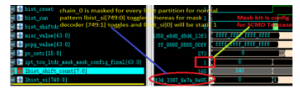
Figure 9: Scan chain mask decoder testcase result
4.4. MISR Expose at PAD Testcase
LBIST controller logic/Integration, reset and clocks of the respective partitions, verified at lbist_fast_clk = 320MHz & lbist_slow_clk = 80 MHz frequencies along with MISR value is exposed at PAD during end of the pattern count using lbist_misr_word_sel bit to expose 1st 32 -bit and later 32 -bit values respectively. As show in Figure 10 MISR value DCCF_7DA6_225C_9279 at program counter value 272 is exposed on PAD pins using lbist_misr_word_sel (0/1).
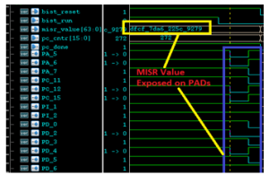
Figure 10: MISR exposed at PAD testcase result
5. Conclusion
The proposed methodology for verifying LBIST implementations at RTL in SoCs is not a replacement for gate level verification of LBIST implementations, with this approach a significant effort and design cycle time can be reduced by moving the verification process early into the SoC design cycle. The results are proven with measurable improvements on real design where the flow/methodology was implemented and helped in identifying the bugs & fixing them before logic freeze, thereby avoiding ECOs.
- Andal Jayalakshmi and Tan Ewe Cheong, “A methodology for LBIST logic diagnosis in high volume manufacturing,” 2012 4th Asia Symposium on Quality Electronic Design (ASQED), Penang, 2012, 249-253, doi: 10.1109/ACQED.2012.6320510.
- K. Butler, “ATPG versus Logic BIST -Now and in the Future,” in 2013 IEEE International Test Conference (ITC), Baltimore, Maryland, 2001 1181. doi: 10.1109/ITC.2001.10048
- P. Maxwell, I. Hartanto and L. Bentz, “Comparing functional and structural tests,” Proceedings International Test Conference 2000 (IEEE Cat. No.00CH37159), Atlantic City, NJ, USA, 2000, 400-407, doi: 10.1109/TEST.2000.894231.
- S. Carbonara, P. Bernardi and M. Restifo, “A Hybrid In-Field Self-Test Technique for SoCs,” 2019 14th International Conference on Design & Technology of Integrated Systems In Nanoscale Era (DTIS), Mykonos, Greece, 2019, 1-6, doi: 10.1109/DTIS.2019.8735075..
- International Standard – IEC61508 – Functional safety of electrical/electronic/programmable electronic safety-related systems, International Electrotechnical Commission, 2010.
- ISO Standard 26262, Part 5, “Road vehicles— functional safety,” 24 May 2016.
- Y. Sato et al., “A circuit failure prediction mechanism (DART) for high field reliability,” 2009 IEEE 8th International Conference on ASIC, Changsha, Hunan, 581-584, 2009, doi: 10.1109/ASICON.2009.5351352.
- H. Iwata and J. Matsushima, “Multi-configuration Scan Structure for Various Purposes,” 2016 IEEE 25th Asian Test Symposium (ATS), Hiroshima, 2016, 131-131, doi: 10.1109/ATS.2016.32.
- S. Wang, Y. Higami, H. Takahashi, H. Iwata and J. Matsushima, “Automotive Functional Safety Assurance by POST with Sequential Observation,” in IEEE Design & Test, 35(3), 39-45, June 2018, doi: 10.1109/MDAT.2018.2799801.
- Wu-Tung Cheng, Manish Sharma, T. Rinderknecht, Liyang Lai and C. Hill, “Signature based diagnosis for logic BIST,” 2007 IEEE International Test Conference, Santa Clara, CA, 2007, 1-9, doi: 10.1109/TEST.2007.4437703.
- M. Abramovici, M. A. Breuer, and A. D. Friedman, “Digital System Testing and Testable Design”, AT&T Bell Laboratories and W. H. Freeman and Company, 1990.
- H. D. Schnurmann, E. Lindbloom and R. G. Carpenter, “The Weighted Random Test-Pattern Generator,” in IEEE Transactions on Computers, C-24(7), 695-700, July 1975, doi: 10.1109/T-C.1975.224290.
- G. Kiefer and H. -. Wunderlich, “Using BIST control for pattern generation,” Proceedings International Test Conference 1997, Washington, DC, USA, 1997, 347-355, doi: 10.1109/TEST.1997.639636.
- Y. Maeda, J. Matsushima and R. Press, “Automotive IC On-line Test Techniques and the Application of Deterministic ATPG-Based Runtime Test,” 2017 IEEE 26th Asian Test Symposium (ATS), Taipei, 237-241, 2017, doi: 10.1109/ATS.2017.52.
- M. Sadi, G. K. Contreras, J. Chen, L. Winemberg and M. Tehranipoor, “Design of Reliable SoCs With BIST Hardware and Machine Learning,” in IEEE Transactions on Very Large Scale Integration (VLSI) Systems, 25(11), 3237-3250, Nov. 2017, doi: 10.1109/TVLSI.2017.2734685.
- P. Wohl, J. A. Waicukauski, G. A. Maston and J. E. Colburn, “XLBIST: X-Tolerant Logic BIST,” 2018 IEEE International Test Conference (ITC), Phoenix, AZ, USA, 1-9, 2018, doi: 10.1109/TEST.2018.8624738.
- E. Moghaddam, N. Mukherjee, J. Rajski, J. Solecki, J. Tyszer and J. Zawada, “Logic BIST With Capture-Per-Clock Hybrid Test Points,” in IEEE Transactions on Computer-Aided Design of Integrated Circuits and Systems, 38(6), 1028-1041, June 2019, doi: 10.1109/TCAD.2018.2834441.
- LBIST Architect process guide Manual Mentor Graphics, Software Version 2018.1.
No related articles were found.