Low Power Fast Settling Switched Capacitor PTAT Current Reference Circuit for Low Frequency Applications

Adv. Sci. Technol. Eng. Syst. J. 5(6), 865–870 (2020);
 DOI: 10.25046/aj0506103
This paper presents a low voltage, low power, fast settling switched capacitor based Proportional to Absolute Temperature (PTAT) current reference circuit. Unlike in a conventional resistor based PTAT current source, the proposed circuit saves a significant amount of silicon area on chip and hence the circuit becomes less susceptible to process variations. It creates a reference current of 1 nA from a 0.5 V power supply at room temperature (27°C). It has PTAT characteristics in the temperatures from 10°C to 80°C. The circuit draws a very low power of 1.5 nW and exhibits a good supply voltage sensitivity of 3.2 %/V. A startup circuit connected to the PTAT source improves the transient response by reducing the settling time. To test the PTAT current reference circuit, a low power log-domain filter which can be used for biomedical applications is realised and biased with the proposed PTAT current source. Results show that the filter cutoff frequency is constant over temperature variations. The CMOS technology used for designing the circuits is UMC 65 nm and tool used for simulations is Cadence Virtuoso.
1. Introduction
Portable and wearable/implantable devices are gaining worldwide acceptance among consumer/biomedical electronics. Circuit de- signs in such devices have a bottleneck on power dissipation and chip area. Log-domain circuits are one of the best possibilities in ex- ploring low power, high dynamic range analog designs. Log-domain filters and transconductance-capacitor (Gm C) filters can be used in biological data acquisition system which involves low frequency signals like ECG (electrocardiogram) and EEG (electroencephalo- gram). Since the transistors in these log-domain filters are working in sub-threshold mode of operation (weak-inversion), a low cutoff frequency can be achieved with low values of bias currents (order of nA). This paper is an extension of work originally presented in [1].
The cutoff frequency ( fo) of log-domain and Gm C filters is given by (1) [2, 3]. where k, T and q have their usual meanings.
Equation (1) shows the direct relation between cutoff frequency and bias current. Io is usually generated from a current reference circuit. The current reference should be stable against variations in process and supply voltage. Supply voltage sensitivity is the parameter which shows the stability of the current reference against supply voltage variations. Lower supply voltage sensitivity indicates a better current reference. Depending on the mode of operation of transistors in the circuit or the topology of the filter architecture, the current reference can be a temperature independent or Propor- tional to Absolute Temperature (PTAT) current reference. From (1) and (2), in log-domain and Gm C filters, it is evident that fo has an inverse relationship with temperature. To fix this problem, Io is generated in such a way that it has also a linear relationship with temperature. Thus a PTAT current reference is used to bias log-domain/Gm − C filters. As a cumulative effect, the filter cutoff

where η, Io and VT are sub-threshold slope factor, bias current and thermal voltage respectively. Equation (2) gives the expression for thermal voltage.
frequency remains constant over temperature variations.
Many PTAT current reference designs are explored in the lit- erature. Beta-multiplier based circuits discussed in [4]–[5] have adequate PTAT current characteristics. However, to generate low reference currents under low supply voltage for low frequency fil- ters used in biological data acquisition system, larger values of
resistors are needed which occupies large area on chip. Moreover the control over temperature coefficient of resistance also becomes difficult. A comprehensive research has been carried out on the region), (3) can be approximated to (4). conventional PTAT designs to tackle such shortcomings [6]–[7]. In [7], self-cascode transistors are used instead of resistor. This improves supply variation rejection, but linearity in current versus temperature characteristic has been compromised. In [8], compos- ite transistors are used in the PTAT circuit to enhance the supply voltage sensitivity, but large resistor values are needed to generate smaller currents. In [2, 9], switched capacitors are used in place of resistor. But PTAT current is generated from PTAT voltage us- ing opamp circuits like voltage to current converter which in turn increases the overall power dissipation of the circuit. [1] shows a good switched capacitor based PTAT reference. But the settling time of the reference current is compromised.
Settling time of current reference becomes a significant aspect especially in high speed applications. When the settling time of the reference current increases, the circuit which uses this reference current to generate its bias current also takes a significant amount of time to settle its bias current to steady state value. In case of a filter used in a wireless communication system, it takes a significant time to fix its cutoff frequency which may lead to attenuation of relevant
signal information. For example, the circuit presented in [1] requires 8 ms to stabilise its current which means that it takes around 8 ms for the subsequent filter to fix its cutoff frequency which is biased by this reference current source. This work proposes a feasible solution
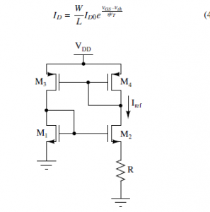
Figure 1: Beta-multiplier circuit
From Figure 1, the reference current Ire f which is also the drain current of M2 (ID2) can be written as (5). to this problem.
In this paper, a fast settling PTAT current source is proposed.
A startup circuit added to the PTAT source improves the settling time of reference current. The proposed circuit exhibits good PTAT characteristics and better stability against power supply fluctuations. This can be used to bias low frequency filters in biomedical appli- cations. A low power log-domain filter is also designed and biased using the proposed PTAT current source. Results show that the cutoff frequency of the filter remains constant irrespective of tem- perature variations. This paper is organized as follows. Details of the proposed PTAT circuit along with the results are given in Section
- Log-domain filter realisation and filter response are detailed in Section 3. Finally conclusions are drawn in Section 4.
2. Proposed Improved PTAT Reference
When transistor operates in weak-inversion region, its drain Voltage across resistor R (VR) can be given as (6).A conventional beta-multiplier based current source circuit [5] is shown in Figure 1. Depending on the mode of operation of transis- tors, it can be a constant-Gm biasing circuit [5] or a PTAT current source. It acts as former if all the transistors work in strong-inversion saturation region (VGS > Vth and VDS VGS Vth) and as latter if all the transistors work in weak-inversion saturation (VGS < Vth and VDS ≥ 3VT ).

Using (4), gate-source voltages of M1 and M2 can be expressed as (7) and (8) respectively.
Vth2j can be written as (9) [11] to include the body effect of By substituting (7) and (8) in (6) and by assuming Vth1 = Vth2, VR can be derived as following.
Thus, Ire f can be expressed as (11). current [10] can be expressed as following.
Assuming R is thermally stable, Ire f is directly proportional to
where ID0 = µnCox(η 1)VT 2; µn and Cox are electron mobility and gate oxide capacitance per unit area respectively. Other terms have their usual meanings. For VDS ≥ 3VT (weak-inversion saturation temperature thereby giving PTAT characteristics. For lower val- ues of currents (order of nAs), large values of resistors are needed. For example, to generate a reference current of 1 nA using circuit shown in Figure 1, a 10 MΩ resistor is required if p is chosen as 1.5. To accommodate such large resistors on chip, huge area is needed which makes the circuit more process dependent, hence reducing the accuracy of Ire f . In a typical SoC (System-on-Chip), where digital circuits and analog circuits co-exist together, a stable and precise clock will be available. In such systems, the resistor R in Figure 1 can be replaced by a switched capacitor driven by this clock which significantly enhances accuracy of Ire f . Improved PTAT current reference

Figure 2: Block diagram
The entire block diagram of the circuit setup explained in this paper is shown in Figure 2. The startup circuit is added to the PTAT current generator to reduce the settling time of Ire f thereby improving the transient response.
By substituting Req (12) in place of R in (11), we get (13).
![]()
From (13) it can be seen that, Ire f is directly proportional to C1.
If fclk and p are chosen properly, smaller capacitor values can be obtained for the currents in the order of nA.
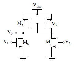
Figure 4: Error amplifier
The purpose of error amplifier which is shown in Figure 4 is to make the drain voltages of M1 and M2 equal thereby making currents through them equal. This kind of biasing minimises the de- pendency of Ire f on VDD which improves supply voltage sensitivity. It takes around 8 ms for the reference current to settle to the steady state value of 1 nA in the circuit presented in [1]. To reduce this delay, a startup arrangement comprising of M10, M11 and CS is added to the circuit. A similar kind of startup circuit is discussed in [12]. In Figure 3, when the circuit is switched on and before it reaches the steady state, initially the gates of M1,2 and M3,4 are at zero volt and VDD respectively. Assuming zero initial voltage across
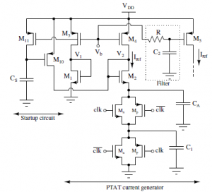
Figure 3: Proposed improved PTAT current reference
The transistor level implementation of PTAT current reference along with startup arrangement is shown in Figure 3. In the pro-
the capacitor CS , M10 turns on and pulls up the gates of M1,2 to VDD. M1,2 start conducting and Ire f rises. Then, potential at the gates of M3,4 drops and M11 turns on. CS starts to charge towards VDD and potential at the gate of M10 increases and once the circuit reaches steady state, M10 turns off. M10 and M11 do not have a static current path from VDD to ground. Hence startup circuit dissipates zero static power.
Value of capacitor CS and sizes of M10 and M11 determine how fast startup circuit can initialise the main circuitry and how fast it can be disconnected once main circuitry reaches the steady state. Transistors M10 and M11 operate in linear region and the linear on resistance of these transistors are given by (14).

posed circuit, every transistor is working in weak-inversion region. The value of p is chosen as 1.5 which means that the size of M2 is 1.5 times the size of M1. A switched capacitor comprising of capacitor C1 and transmission gate switches (Mn and Mp) is used in place of resistor. Mp is selected 4 times larger than Mn in the transmission gate so that its on resistance does not depend on the voltage across it. Two clocks (‘clk’ and ‘clk’) which are complementary to each other and having frequency fclk are used for the switching operation. When ‘clk’ becomes high (‘clk’ becomes low), capacitor C1 charges and when ‘clk’ becomes low (‘clk’ becomes high), it discharges. The average resistance (Req) of the switched capacitor is given as in (12) [5].
How fast startup circuit is switched on depends on how fast transistor M10 turns on. The on time of M10 is limited by the input capacitance of M10 which comprises of gate to source and gate to drain capacitances. By properly choosing the size of M10, the on time can be optimised.
When it comes to disconnection of startup circuitry, assuming M11 as a linear resistance given by (14), the RC time constant (τ) of the branch consisting of M11 and CS is given by (15).
![]()
When capacitor CS charges above the voltage (VDD Vth), M10 turns off. (VDD Vth) is approximately 150 mV in this design and time for CS to charge to this voltage (30 % of final value) from 0.5 V supply through M11 is nearly 0.4τ.
A low pass filter which comprises of R and C2 is added to main- tain the ripple content in the output reference current within the accepted level. Capacitor C2 is chosen as 0.1 pF and resistor R is tuned to obtain the ripple content in Ire f less than 1 %. To remove high frequency noise during switching operation, capacitor CA is used at the source of M2. A 100 kHz clock is selected for this work. The capacitors, C1, CA, CS are taken as 0.8 pF, 10 pF, 1 pF respectively. By substituting (13) in (1), fo can be expressed as (16).

From (16), it can be seen that fo is independent of temperature.
2.1 Simulation results
The proposed circuit is designed using UMC 65 nm CMOS process with a supply voltage of 0.5 V. Periodic Steady State (PSS) analysis is carried out to plot the reference current. Figure 5 shows the out- put current generated (1 nA) for one clock period (10 µs) at room

Figure 7: Ire f for different supply voltages

Figure 8: Ire f across the process corners
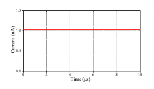
Figure 5: Ire f at VDD= 0.5 V
Figure 6 shows Ire f variations when temperature is varied from linearly with temperature and thus has a good PTAT characteristics over the range of temperature.

Figure 9: Transient response of the current flowing through M2
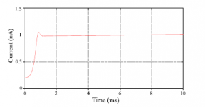
Figure 10: Transient response of the current flowing through M5
Ire f is plotted for different values of VDD at room temperature as shown in Figure 7. Ire f is 0.996 nA and 1.018 nA for VDD of 0.4 V and 0.9 V respectively. The supply voltage sensitivity of Ire f is found to be 3.23 %/V by considering these extreme values.
Figure 8 plots Ire f for various process corners at room tempera- ture and VDD = 0.5 V. Ire f deviates maximum in ss and ff corners (1.034 nA and 0.968 nA). The maximum deviation is less than 3.6
The current flowing through the source of M2 is shown in Figure
- It has ripples having peak to peak magnitude of approximately
where Iin contains both dc current Idc and input current Isignal. IK is the current flowing through M3 which contains both capacitor current IC and Idc. Iout is the output current. Equation (19) can be realized using a translinear loop having four transistors. These equations can be implemented in the form of a translinear circuit as shown in Figure 11 [15]. 0.1 nA. The ripple free current flowing through M5 is shown in Figure 10. The settling time is found to be approximately 1 ms.
Table 1: Comparison of the proposed work with other similar works
|
The improved PTAT reference consumes a power of 1.5 nW at room temperature from a supply voltage of 0.5 V. The proposed circuit along with existing PTAT current references in the literature are listed in Table 1 and a fair comparison is done. The proposed
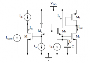
Figure 11: First order log-domain filter
In this circuit, the MOSFETs M1–M4 form the translinear loop. These transistors are working in sub threshold saturation region. The cutoff frequency of the filter can be tuned by varying the DC current and is given by following [16].
PTAT circuit functions under the lowest supply voltage and has a very low supply voltage sensitivity and settles faster than [1] (nearly 87 % improvement in settling time).

3. Log-Domain Filter Realization
The proposed PTAT current source shows excellent PTAT character- istics. To verify this, a low frequency log-domain filter is designed and biased with the proposed switched capacitor based PTAT cur- rent reference. This log-domain filter can be used in low power biomedical applications like processing of ECG, EEG signals. The expectation is that the cutoff frequency of the filter remains the same irrespective of the variations in temperature.
The transfer function of a first order low-pass filter is The ideal DC current sources shown in Figure 11 can be re- placed by current sources implemented using MOSFETs. In this work Idc is taken as Ire f (1 nA). The cutoff frequency of 100 Hz is obtained by choosing C=37 pF. time domain differential equation is given by
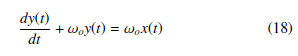
where x(t) and y(t) represent the input and output currents of the filter respectively. By solving the differential equations and relating the current-voltage in transistor operating in subthreshold operation, we get
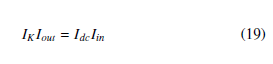
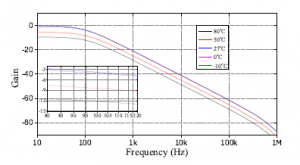
Figure 12: AC response of the filter biased with temperature independent current reference
3.1 Simulation results
The filter is designed using UMC 65 nm CMOS technology with a supply voltage of 0.5 V. For a comparison, Idc is generated from a temperature independent current reference and ac response of the filter is plotted. Figure 12 shows the variation of cutoff frequency in the temperatures ranging from 10◦C to 80◦C. The maximum deviation is found to be 16 %. To verify the PTAT characteristics, Idc is generated from the proposed PTAT source and ac response is plotted. Figure 13 shows that deviation of cutoff frequency is negligible and maximum deviation is found to be less than 2 %. The band transitions are enlarged in corresponding inset graphs. Table 2 shows the deviation of filter cutoff frequency for both temperature independent and the proposed PTAT references.

Figure 13: AC response of the filter biased with PTAT current reference
Table 2: Cutoff frequency deviation
| Temperature
(◦C) |
Cutoff frequency (Hz) | |
| Temp. independent | PTAT | |
| -10 | 116 | 101.9 |
| 0 | 107 | 101.2 |
| 27 | 100 | 100 |
| 50 | 93 | 99 |
| 80 | 88 | 98.4 |
Table 3 lists the parameters of the filter designed in this work.
Table 3: Parameters of the filter
| Technology | 65 nm CMOS |
| Supply voltage | 0.5 V |
| Power | 2.5 nW |
| Cutoff frequency | 100 Hz |
| DC gain (at 27◦C ) | 0.94 |
| Iin pp at 25 Hz for 1% THD | 0.82 nA |
| Input referred noise from 1 Hz to 100 Hz | 3.26 pArms |
| Dynamic range | 48 dB |
4. Conclusion
This paper proposes a low voltage, low power, fast settling switched capacitor PTAT current reference circuit. Settling time is reduced with the aid of a startup circuit. The PTAT circuit exhibits good PTAT characteristics in the temperatures ranging from 10◦C to 80◦C while operating under a very low power. The circuit is less susceptible to power supply fluctuations and can work at supply voltages as low as 0.4 V. To test the PTAT source, a low power log- domain low frequency filter is also designed and biased with PTAT reference. Simulation results imply that the filter cutoff frequency remains unchanged irrespective of temperature variations and this validates the theory explained in the paper.
- H. G. Rao, S. Rekha, “A 0.5 V, 1 nA Switched Capacitor PTAT Current Refer- ence Circuit,” in 2019 IEEE Conference on Modeling of Systems Circuits and Devices (MOS-AK India), 51–54, 2019.
- A. Gerosa, A. Maniero, A. Neviani, “A fully integrated dual-channel log- domain programmable preamplifier and filter for an implantable cardiac pace- maker,” IEEE Transactions on Circuits and Systems I: Regular Papers, 51(10), 1916–1925, 2004.
- R. Schaumann, H. Xiao, V. V. Mac, Design of Analog Filters 2nd Edition, Oxford University Press, Inc., 2009.
- E. Vittoz, J. Fellrath, “CMOS analog integrated circuits based on weak inver- sion operations,” IEEE journal of solid-state circuits, 12(3), 224–231, 1977.
- P. R. Gray, P. Hurst, R. G. Meyer, S. Lewis, Analysis and design of analog integrated circuits, Wiley, 2001.
- B. Razavi, Design of analog CMOS integrated circuits, Tata McGraw-Hill, 2002.
- L. Magnelli, F. Crupi, P. Corsonello, C. Pace, G. Iannaccone, “A 2.6 nW, 0.45 V temperature-compensated subthreshold CMOS voltage reference,” IEEE Journal of Solid-State Circuits, 46(2), 465–474, 2011.
- F. Serra-Graells, J. L. Huertas, “Sub-1-V CMOS proportional-to-absolute tem- perature references,” IEEE Journal of Solid-State Circuits, 38(1), 84–88, 2003.
- E. M. Camacho-Galeano, C. Galup-Montoro, M. C. Schneider, “A 2-nW 1.1-V self-biased current reference in CMOS technology,” IEEE Transactions on Circuits and Systems II: Express Briefs, 52(2), 61–65, 2005.
- H. G. Rao, C. B. M. Mansoor, S. Rekha, “A 0.8 V, 5 nA PTAT current reference circuit with improved supply voltage sensitivity,” in 2019 Global Conference for Advancement in Technology (GCAT), 1–4, 2019.
- S. Malik, M. Schlarmann, R. Geiger, “A low temperature sensitivity switched- capacitor current reference,” in Proceedings of the European Conference on Circuit Theory and Design (ECCTD), 269–272, Citeseer, 2001.
- Y. Tsividis, C. McAndrew, Operation and Modeling of the MOS Transistor, Oxford Univ. Press, 2011.
- L. H. Ferreira, T. C. Pimenta, R. L. Moreno, “An ultra-low-voltage ultra-low- power weak inversion composite MOS transistor: Concept and applications,” IEICE transactions on electronics, 91(4), 662–665, 2008.
- S. Kumar, H. G. Rao, S. Rekha, “A 1-V, 8.6-nA Resistor-less PTAT Current Reference with Startup Circuit,” in 2018 15th IEEE India Council International Conference (INDICON), 1–4, 2018.
- Y. Osaki, T. Hirose, N. Kuroki, M. Numa, “1.2-V supply, 100-nW, 1.09-V bandgap and 0.7-V supply, 52.5-nW, 0.55-V subbandgap reference circuits for nanowatt CMOS LSIs,” IEEE Journal of Solid-State Circuits, 48(6), 1530– 1538, 2013.
- V. Jorge, A. L. Aita, “A 1-V PTAT current reference circuit with 0.05%/V current sensitivity to VDD,” in Proceedings of IEEE International Symposium on Circuits and Systems (ISCAS), 502–505, 2016.
- A. Patil, C. B. M. Mansoor, H. G. Rao, S. Rekha, “Low power log-domain filter,” in 2019 IEEE 16th India Council International Conference (INDICON), 1–4, 2019.
- J. Mulder, W. A. Serdijn, A. C. van der Woerd, A. H. van Roermund, Dy- namic translinear and log-domain circuits: analysis and synthesis, volume 481, Springer Science & Business Media, 2012.