
Design and Implementation of Quad-Site Testing on FPGA Platform
Volume 5, Issue 5, Page No 789-798, 2020
Author’s Name: Basavaraj Rabakavi1,a), Saroja V Siddamal2
View Affiliations
1Department of Electronics and Communication, Government Engineering College, Haveri, 581110, India
2School of Electronics and Communication, KLE Technological University, Hubli, 580021, India
a)Author to whom correspondence should be addressed. E-mail: bsrabakavi@gmail.com
Adv. Sci. Technol. Eng. Syst. J. 5(5), 789-798 (2020); ![]() DOI: 10.25046/aj050596
DOI: 10.25046/aj050596
Keywords: Multi-Site Testing, Concurrent Testing, Propagation Delay, Quad IC Tester, VLSI, ATE, FPGA, IC Packages

Export Citations
As manufacturing efficiency has become a main focus of today’s business, it is very critical to surge the throughput by developing different test strategies. With throughput, testing cost also has been recognized as the major challenge in the future of leading semiconductors. Reducing test time is a significant effort to maximize throughput as the complexity increases in future generation outcomes and devices. So, low-cost Automatic Test Equipment (ATE) with parallel test can be promoted as the obvious solution for challenges said above. In parallel testing, multiple devices-under-test (DUT) can be tested at a time that enhances way of testing by increasing product flow, limiting gross test times, and efficient usage of tester. The proposed Integrated Circuit (IC) tester is used to implement multi-site testing (Quad-Site testing) and concurrent testing. It exhibits multi-site efficiency which substantially enhances the throughput by reducing test time. Modular, re-configurable test system provides cost-saving solution. To confirm these effects, authors have presented experimental results for Quad site testing of different ICs namely Decoder, Buffer, Multiplexer and Logic gates. This portable IC Tester handles variety of IC packages like Dual Inline Package (DIP), Small Outline Integrated Circuit (SOIC), Thin Shrink Small Outline Package (TSSOP). With functional test, the proposed tester also verified the AC Parametric tests (i) Propagation Delay is 20ns (ii) Operating frequency with 50MHz for Decoder IC (74HC138). The proposed IC tester consumes 70% less power and throughput enhanced by 11% compared to existing IC testers.
Received: 17 August 2020, Accepted: 21 September 2020, Published Online: 12 October 2020
1. Introduction
This paper is an extension of previous work originally presented in the 3rd IEEE International Conference on Electrical, Electronics, Communication, Computers and Optimization Techniques [1]. Integrated Circuits which are more commonly known as ICs, are the central components of every electronic circuits present in modern times. Though it is one of the most important and vital part of the circuit, these ICs are most prone to be the cause of the malfunctioning of the whole design. With the advent of the complex integrated circuits, the problem arises after production of digital circuits to verify its functionality towards the meeting specifications. While delivering a product to market, testing plays an important role in the overall process. It is impossible to dispatch quality chips to the customer without proper testing. However, testing cost is also part of the overall product cost. Since it is very essential to test the IC before actually using them in any applications, an IC tester has been developed in order to eliminate the complex process of circuit troubleshooting [2, 3].
1.1. Types of testing
There are three types of testing: (i) Functional (ii) Parametric (iii) Structural tests. Functional testing is carried out by assigning specific test vectors to device under test, measuring the circuit response and device’s functionality. Parametric tests are performed to determine the basic electrical characteristics of the device. DC parametric tests verify threshold levels of voltages and currents, in addition to open/short circuit tests and DC parameters are independent of time. AC characterization tests verify time dependent properties like propagation delays, transition signals (rise and fall) and operating frequency range. In structural testing, test inputs are designed to find out particular faults that might have occurred in circuit due to manufacturing deficiencies. During a structural verification, it is assumed that the circuit design is proper and the intention of the testing is to detect faults because of failures in processing [4].
1.2. Stages of testing
There are four different stages of Very Large-Scale Integration (VLSI) testing; (i) Characterization (ii) Production (iii) Burn-in (iv) Incoming inspection. A characterization test measures the true operating limit values of the product. Before manufacturing, this test is carried out on a current design. Manufacturing test undergoes for smaller duration but checks all relevant parameters of the product. This test covers maximum number of standard faults but all expected functions may not be covered by test inputs. Burn-in makes sure the safety of devices by verifying the devices for longer duration, either continuously or regularly, and causing the wrong products to really fail. System manufacturers carry out incoming inspections on the purchased devices before incorporating them into the system [5].
1.3. Traditional method of testing
Everywhere digital circuits are growing consistently in case of both quantity and complexity. Meantime, automated circuit testing is going tougher, costly and critical. Manufacturing test plays a key role in ensuring the standard of the ICs supplied to the consumer. While ICs consistently integrating greater Built-In Self-Test (BIST) approaches, external testing instrument is still required in case of manufacture testing such as reading of specific configuration data or IC characteristics for assessment of ICs performance. Manufacturing test is carried out by advanced ATE, designed to work consistently with high quality standards. These High performance ATEs (HATEs) are costly and high-power consuming machines [6].
Now a day, there are two major types of ATE instruments exist in market: Highly sophisticated ATE and Low-price ATE. Instruments belongs to highly sophisticated ATEs are Verigy, Advantest, Teradyne etc. and normally used in testing industries and their functioning is closely related to manufacturing stage. Highly sophisticated ATE manufactured by industries such as Advantest are costlier (millions of dollars) and need specialized technical skills to be utilized with precision [7]. Costs can be decreased much further by using Field Programmable Gate Array (FPGA) based hardware and computer software in combination. The advances in FPGA technology supports the development of FPGA based low cost ATE. Low cost FPGA based ATE case study can perform functional tests of digital circuits [8].
1.4. Advanced method of testing
Present product trends need greater parallelism in testing methods and flows of VLSI. The overall price of both wafer and production testing will be increased by high-end ATE. So, the increased price of System on Chip (SoC) testing and the ATE cost are two major worries for the semiconductor companies. Multi-site testing with available low-price ATEs is the only solution to resolve this issue by reducing the cost of test. In both wafer and package stage testing methods, multi-site testing can be utilized [9]. Increasing the degree of parallelism can reduce testing price by decreasing the recognizable test time for every product. Multi-site testing is a classic parallel test method where many devices are tested at the same time. Concurrent method of testing is another parallel technique, in which two or more operational modules related to same product are verified in parallel. If the product and test design engineers are able to make sure that independence in their designs individually, then the testing can be carried out simultaneously [10].
1.5. Necessity
The VLSI circuit manufacturer cannot guarantee the defect free integrated circuits (ICs). It is not feasible for small-scale industries investing huge amounts of money to buy sophisticated IC testers. Similarly, directly replacing ICs mounted on a board may not be desirable solution to repair a malfunction. The limitations of high end ATE machines are high price instrument, imprecision and need large memory. Therefore, all the limitations indicated above lead to the way for designing a new IC tester with low price, high accurate with maximum speed, otherwise advantages of semiconductor technology are purposeless [11].
1.6. Contributions
In previous work [1], Dual IC testing of digital ICs was implemented with feature of functionality test only. In this paper, work is extended to perform propagation delay test, operating frequency test with Quad IC testing simultaneously and also to analyze the power consumption and throughput of the proposed testing system. This paper describes a FPGA based reconfigurable, inexpensive, high speed, indigenous testing platform for standard digital ICs (74/54- types). This IC tester can be implemented with low budget for small or medium-scale industry customers of these ICs & offers fast and detailed check-out functions with minimal operator action.
Rest of the paper is organized as follows. Section 2 describes motivation for designing the multi-site tester. In section 3, concept of multisite testing is discussed. Proposed methodology is described in section 4. Results are discussed in section 5 and followed by the conclusion.
2. History and Motivation
2.1. Manufacturing Process Defects
Various types of defects can occur during the manufacture of any circuit, this leads to errors. There are four categories of defects as age defects, process defects, material defects and package defects. Process defects and material defects arise due to material imperfection during manufacture of the circuit. Age defects arise due to usage of device for longer duration and also with over time. Physical assembling of the circuit can cause package defects and other defects can be caused due to opening or breakage of pins [12]. Addition to mentioned defects, the person working on testing can also cause defects by testing the devices with incorrect test program or sometimes testing procedure itself can cause faulty components. Test instrument without calibration leads to wrong results. The person working on production lab can put good devices in the incorrect bin and also possible that a good device can be stamped with wrong part number [13].
2.2. Need for FPGA
Earlier digital IC testers were implemented using micro-processor or microcontroller family. Test vectors stored in the memory as lookup table are assigned to every IC to be tested. Reconfigurable logic system has programmable interconnections to allow the user to perform required operation within it and it is known as Programmable Logic Device (PLD) or FPGA. Now a day, PLD’s logic density has become more sufficient to implement lot of data processing operations within it. Even though ASICs achievement is more compared to PLD, when same application is realized in both devices, PLD’s re-configurability has many advantages. PLD System with applications having high parallelism can be quicker more than hundred times than the microcontroller-based system. FPGA produces the test patterns by using Test Pattern Generator (TPG), rather than storing the test patterns as a lookup table for specific IC [11, 14].
FPGAs provide a greater number of tested devices in the specified period of duration. FPGA supports high standard of parallelism while generating various test vectors that varies in properties, ranging from simple digital circuits to highly complicated digital products [15]. FPGAs have many benefits which consist of more speed, large number of input and outputs, less power consumption, less size, enhanced time-to-market and increased flexibility and re-configurability. The number of I/O pins differs between one device to another device. Additionally, the interconnection between DUT pins and test equipment also varies from device to device. Hence, to perform the tests, the test device must be wise enough to handle pin configurations and input/output allocation of the DUT. For I/O handling issue, FPGA based ATE with reconfiguration property is the solution [16].
2.3. Tester requirement
All devices are not identical even though they pass in production tests. When actually used in the field, some will function for longer time and some will fail early. Out of four testing stages, incoming inspection is one of them. Incoming inspection can be conducted for arbitrary samples depending on the standard device and the system specifications. As the cost of incoming inspection is much less compared to the cost of testing in assembled system, the incoming inspection of components is much necessary in the industry [5]. To carryout incoming inspection, digital IC testers are required in various electronics laboratories and industries during design, after manufacturing stage of different electronics devices [6]. As small-scale industries or assembly housing units cannot offer large amount of investment for high end ATEs, less price ATE or IC testing device is the solution for incoming inspection. The requirement of low-cost tester is not only in industries but also in the academics. The low-cost tester can be achieved by implementing multisite and concurrent testing.
3. Concept of Multi-site Testing
IC testing is an important method to create insulation between good and poor components to make sure the quality of the outgoing goods. Traditionally single site testing method was used for testing. In single site method one DUT was verified at given instance using ATE [17]. Reduction in the testing cost is the repeated challenge of the semiconductor manufacture, and the test time has become important part of the Cost of Test (CoT). Because of high competency, system design companies have low profit margins in market, a continuous check on the low average price and quick time to market is very important [18]. Multi-site parallel testing provides the greatest enhancement to throughput on test, irrespective of the particular task. The multi-site parallel test concept has throughput advantages over traditional parallel test methods. In traditional parallel testing, multiple devices are tested on the same site. Once all testing on one site is completed, the prober indexes to the next site. By contrast, the multi-site parallel testing method is performed on multiple devices on different (multiple) sites at the same time as shown in the Figure.1. This eliminates all dead time between tests, and means there is no waiting for any one test to complete before the prober indexes to the next site. The test program is written so that at a time all similar DUTs are tested.
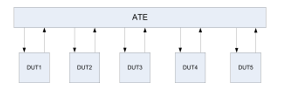
Figure 1: Multi-Site with parallel DUT testing
The total time taken for the group of devices tested at the same time is the addition of the index time ti and the production test time tp as shown in the Figure 2. The index time ti is the time duration to build contact between the bonding pads of the DUTs and the probe interface by making proper positioning. The index time ti differs on the type of probe station used and it is fixed for each probe station. A normal value of ti is 0.7sec [19]. The production test tp is the sum of different tests performed on DUT which may include functionality and characterization test.
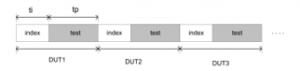
Figure 2: Testing time of DUT consists of index time ti and test time tp
If there is no waiting time between replacement of chip being tested is completed with new chip to be tested, then only index time was considered as valid. If immediate replacement of a new chip after the chip being tested is completed, then the indexing time is ignored. If there are no issues like tester downtime and chip contacting problems then test time was considered as valid [20]. The total testing time of a device Ts (Single site test time) can be written as shown in equation (1).
Ts = ti + tp (1)
The Multi-Site-Testing is the test method for simultaneous testing of multiple similar DUTs on single ATE. The test time spent on one device of the Multi-Site-Test is 1/N of the Single-Site-Test. So, Multi-Site-Test testing time is close to time taken by Single-Site-Test. Earlier this test method was utilized for the testing memory devices, but now almost all semiconductor devices are tested with this strategy to decrease the testing cost. The Multi-Site-Test needed times of the tester resources. Relationship between Multi-Site-Test and Single-Site-Test test timings can be given by Multi Site Efficiency (MSE). MSE is calculated as shown in equation (2).
MSE = ((N – Tm/Ts)/(N-1))x100 (2)
Where N is the number of devices that can be tested in Multi-Site test, Tm is time consumed for Multi-Site-Test and Ts is time taken for Single-Site-Test. Generally, Digital circuits MSE is higher than the MSE of analog circuits. i.e. MSE of Digital tests is about 95% and Analog mixed signal MSE is around 60 to 85% [21]. Considering the maximum usage of the ATE, total devices tested per hour i.e. for multi-site testing with N number of devices or throughput can be given as in equation (3).
Dth = (3600 x N)/Tm (3)
4. Proposed Architecture for Quad IC Tester
The proposed architecture of FPGA based Quad IC tester is shown in the Figure 3. It contains FPGA device, devices under test, power supply device and peripheral Interfaces such as switches, LEDs and Displays. In this design, Altera Development board is used for FPGA device (Cyclone II – family) and also for user I/O interfaces. FPGA design consists of various modules as Test Pattern Generation (TPG), Output Response Analyzer (ORA), Input/output compatibility, Frequency Synthesizer and peripheral interface modules.
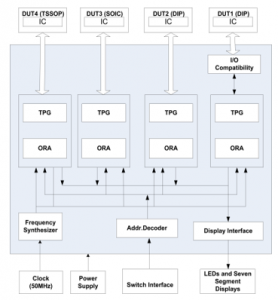
Figure 3: Proposed architecture of Quad IC Tester.
Different test vectors required to test the functionality of the DUT are generated by TPG module. The outputs of the DUT are latched by ORA module to verify with expected ones. If the actual results are similar to the expected results, IC tester displays (PASS), or else (FAIL). Frequency Synthesizer is used to produce various frequencies, which is required for TPG module to generate test vectors and to maintain synchronization among different blocks. As ICs will differ in their Input/Output (I/O) configurations, the I/O compatibility module is required to use single slot for testing different ICs. All the modules are described in the remaining sections.
4.1. Test Pattern Generation
Test Pattern Generation module produces desired test vectors for the device under test. Deterministic, exhaustive, random generations are different ways of producing the test patterns. In present work, exhaustive test patterns are utilized for 100% fault coverage during the testing of IC. In the case of logic gate IC, all quad gates are applied with the same patterns and tested simultaneously. Each different combinational circuit or sequential circuit will have different test patterns generated by Finite State Machine (FSM). Figure 4 shows the FSM for generating test patterns for dual 4:1 multiplexer. This FSM has eight states (S0 to S7) controlled by master clock. FSM is in initial state S0 as long as reset and ebar signals are held high.
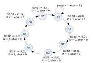
Figure 4: FSM for Generation of Test Patterns for Dual 4:1 MUX
4.2. Output Response Analyzer
The ORA module receives the actual outputs from the DUT and compared with desired values stored in register. Depends on the comparison result, specific bit say R1 will be set as ‘1’ if the result exactly same as desired one, or else it is declared as ‘0’. In view of complex digital circuits, ORA module is used to verify whole data given in truth table or sequence table of DUT’s datasheet with its real outputs, prior to setting of R1 bit. Choice of expected values stored in register is done by setting the switches at the beginning of test, based on the IC inserted in the specific socket. By considering dual 4:1 Multiplexer IC, outputs of multiplexer are captured and stored on every negative edge of input clock into temporarily register i.e. temp [7:0]. This process is continued until input patterns are reached to DUT by FSM in TPG module. Figure 5 shows the FSM for latching the outputs of dual 4:1 MUX.
4.3. Frequency Synthesizer and Input/output Compatibility
The proposed IC tester tests various ICs of different frequencies. Frequency Synthesizer is needed to produce clocks with different frequencies like 2Hz, 0.5MHz, 1.567MHz, 3.125MHz, 6.25MHz, 12.5 MHz, 25MHz. Altera FPGA board consists of 50MHz and 27MHz as master clocks. Binary counters are used to generate various frequencies. Frequency synthesizer module is utilized to calculate propagation delay and operating frequency range of particular IC. Depending upon the modes of operation like user mode or fast mode, specific frequency is selected for IC testing. IC results are monitored using LEDs with help of 2Hz frequency in user mode. Figure 6 shows frequency generation of 25MHz and 12.5MHz, similarly other frequencies are also generated.
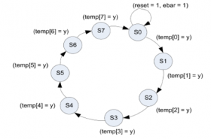
Figure 5: FSM shows output latching of Dual 4:1 MUX
Provision of single slot for testing of various ICs with different I/O connection is the complex problem. If different ICs are to be tested using single socket, then each pin of particular IC need I/O compatibility. This issue is solved by designing I/O compatibility module using multiplexers and tristate buffers. The Figure 7 represents the I/O compatibility logic for single pin. Similarly, all other pins of ICs can be configured as input/output based on the IC selection.
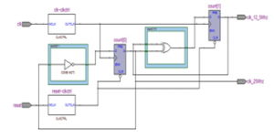
Figure 6: Frequency generation of 12.5MHz and 25MHz
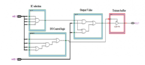
Figure 7: I/O handling logic for single pin of IC
4.4. Propagation delay test and Functional speed test
Propagation delay test is one of the AC Parametric Test of IC. Propagation delay is the addition of switching delay of device and transport delay of interconnects on the track [5]. The process of finding the propagation delay is shown in the Figure 8. Once the test vector of DUT is active i.e. transition from low to high, one pulse is generated. At this time, high frequency counter is started and continues to count till it come across change in output of the device to be tested. The change in output of the device is recognized by pulse generated due to the low to high transition occurs at the device output. Propagation delay is calculated by multiplying the number of counts with time period of master clock used for counter. The equation (4) shows calculation of the propagation delay, where Pd represents propagation delay, C indicates the number of counts from change of input value to the change of output value and T is the time period of the high frequency clock used to run the counter.
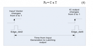
Figure. 8: Process to calculate the propagation delay
Functional Speed Test or Operating Frequency Test of device under test is also one of the AC Parametric tests. Here, the specific test inputs are produced and verified for the performance of the device. The speed at which functionality results of device meet the expected values is called functional speed of the device. The propagation delay test and functionality speed test results are shown in the section 5.
4.5. Quad IC Testing
Most of the existing single IC testers are made up of microprocessor or microcontroller device. The limitations of these testers are sequential execution and a smaller number of input/outputs. In the presented work, the above limitations are overcome by developing test logic with individual FSM for each device. All the FSMs will run in parallel, because of this feature proposed Quad-IC tester can test four different ICs simultaneously.
5. Results and Discussion
The proposed IC tester is designed and developed on target Altera FPGA Development board (Cyclone II – family). The testing logic is developed using Verilog HDL. The design is synthesized using Altera Quartus-II 9.1 tool. Test vectors are produced by TPG modules according to the truth table or sequence table of individual ICs. The functional test of four different ICs, namely Logic gate, Multiplexer, Decoder and Buffer is performed simultaneously and details of the testing is given in Table 1. Simulation results of TPG and ORA modules are verified for all Digital ICs with respect to its functionality through waveforms. All four ICs are tested in parallel with one-time test and loop test facility by selecting switch as 0/1 respectively. Results are verified through LEDs using IC selection values with fast mode or user mode facility. Status of the result shown in the seven-segment display as IC1P (i.e. First IC is PASS).
Functional test of ICs is carried out with different frequencies by frequency synthesizer to find out the testing speed of IC. Buffer IC is tested with four values namely as 0xff, 0xaa, 0x00, 0x55 in a loop test with 50MHz. Similarly, Decoder IC is tested according to its truth table sequence with 50MHz successfully. Logic gate ICs outputs are verified with 12.5MHz. Multiplexer IC is tested for all combinations of test vectors with 6.25MHz successfully. All the ICs are powered with 5V supply. Table 2 shows the operating frequency and total time required to complete the functionality test of particular IC for all combinations of test vectors.
Propagation Delay test is performed on ten ICs individually and measured values of propagation delays of each IC is given in Table 3. The ICs having ‘HC’ (High speed CMOS) symbol in their names operate with both voltages ‘2V’ and ‘5V’. Propagation delay values of ICs differ with respect to supply voltages.
In this work, system clock 50MHz is used to find out the propagation delay. The count value represents the delay between rising edge of test vector to rising edge of gate output. The count value is multiplied with clock period of master clock (i.e. 20ns) which gives the switching delay of the device. In this work, transport delay is considered as negligible (usually in terms of Pico Secs) and it is fixed value. For example, for 74HC86 IC the propagation delay is calculated by using equation (4) i.e. Pd = C x T = 2 x 20ns = 40ns. In which, C is count value and T is time period of 50MHz clock. Similarly, propagation delay is calculated for all other ICs. Out of ten ICs, eight ICs results are almost similar to the respective datasheet values except two ICs (74HC266 and 74HC153). Reasons may be because of EX-NOR IC has open collector pins, the delay depends on pull up resistor values and MUX IC depends upon its switching activities.
Proposed IC tester also aims to test functionality of ICs with low power consumption. The power consumed by testing logic with respect to each IC is given in the Table 4. Power consumption of developed testing logic is calculated using Powerplay Early Power Estimator Spreadsheet provided by respective FPGA IC vendor (Altera Cyclone II spreadsheet- Now Intel). It will be achieved by filling the utilization of FPGA device i.e. LUTs, FFs, Input/output pins used, clock rate and total fanouts details in the spreadsheet of FPGA family.
The top verilog module or integrated module gives overall power consumption for testing four ICs simultaneously. Power consumption calculated using spreadsheet is static or offline method and for top module it is 169mW. Table 5 shows the power consumed by proposed system in real time during Quad IC testing. The power consumed by FPGA board is calculated by multiplying Icc with Vcc (5V). The current Icc is measured through ammeter placed on power supply path of hardware during Quad IC testing and it is 0.30A. Similarly, board power is calculated before downloading the testing logic onto FPGA device. So, the power consumption of testing logic is calculated by subtracting board power consumption (powered on condition i.e. without code) from power consumed during testing of Quad ICs i.e. 1.5W-1.25W = 0.25W. Total power consumed during testing is 1.5W which is less compared to commercial testers. In the Table 6, the power consumption of the proposed tester is mentioned approximately as 2W by considering enhancement of testing logic to cover variety of ICs.
Table 1: Functional test of Quad ICs
| Quad IC Testing (Functionality Test – Simultaneously) | ||||||||
|
Sl. No |
Device Name (IC name) | Package | IC Pins | IC Selection | Fast mode (1)/User mode (0) | Loop test (1)/One time test (0) | Expected Result | Actual Result |
| 1 |
74HC244 (8bit Buffer/Driver) |
TSSOP | 20 | 1 (001) | 0 | 0 | IC1-PASS | IC1-PASS |
| 2 | 74HC138D (3:8 Decoder) | SOIC | 16 | 2 (010) | 0 | 1 | IC2-PASS | IC2-PASS |
| 3 |
74HC153N (Dual 4:1 MUX) |
DIP | 16 | 3 (011) | 1 | 1 | IC3-PASS | IC3-PASS |
| 4 |
SN74HC86N (Quad XOR Gate) |
DIP | 14 | 4 (100) | 1 | 0 | IC4-PASS | IC4-PASS |
Table 2: Operating Frequency test
| Operating Frequency Test | |||
| Sl.No | Verilog Module name | Operating Frequency for Loop Test | Time required complete functionality test (Power supply – 5V) |
| 1 | Buffer module | 50MHz | 80ns (4 values – write and read) |
| 2 | Decoder module | 50MHz | 160ns (8 test vectors) |
| 3 | Gate module | 12.5MHz | 320ns (4 test vectors) |
| 4 | MUX module | 6.25MHz | 1280ns (8 test vectors) |
Table 3: Comparison of Real time Propagation Delays with Datasheet values
| Propagation Delay Test | ||||||||
| Sl. No | Device (IC) | Values measured using Proposed IC Tester (Actual values) |
Values given in Datasheet |
|||||
| Power supply (2V) | Power supply (5V) | 2V | 5V | |||||
|
Count value |
Time taken by devices |
Count Value |
Time taken by devices | Expected values | ||||
| 1 |
74HC86 (EXOR gate) |
2 | 2x20ns = 40ns | 1 | 1×20 = 20ns | 40 | 12 | |
| 2 | 74HC138 (Decoder) | 2 | 2x20ns = 40ns | 1 | 1×20 = 20ns | 40 | 15 | |
| 3 | 74HC244 (Buffer) | 2 | 2x20ns = 40ns | 1 | 1×20 =20ns | 30 | 11 | |
| 4 | 74HC153N (Mux) | 4 | 4x20ns = 80ns | 2 | 2×20 = 40ns | 50 | 17 | |
| 5 |
74LS00 (NAND gate) |
NA | NA | 1 | 1×20 = 20ns | NA | 22 | |
| 6 |
74LS02 (NOR) |
NA | NA | 1 | 1×20 = 20ns | NA | 10 | |
| 7 |
74LS08 (AND) |
NA | NA | 1 | 1×20 = 20ns | NA | 15 | |
| 8 |
74LS32 (OR) |
NA | NA | 1 | 1×20 = 20ns | NA | 15 | |
| 9 |
74LS04 (NOT) |
NA | NA | 1 | 1×20 = 20ns | NA | 10 | |
| 10 | 74HC266 (EX-NOR) | 18 | 18×20 = 360ns | 18 | 18×20 = 360ns | 150 | 30 | |
Table 4: Power Consumption of Testing Logic
| Power Calculation Through PowerPlay Early Power Estimator Spreadsheet (Offline) | |||||||
| Individual Modules | |||||||
| Sl.No | Verilog Modules | Logic | Input/ Output | Clocks | Total (mW) | ||
| 1 | Bufer module | 1 | 36 | 3 | 40 | ||
| 2 | Decoder module | 0 | 32 | 3 | 35 | ||
| 3 | MUX module | 0 | 34 | 3 | 37 | ||
| 4 | Gate module | 0 | 32 | 3 | 35 | ||
| 5 | Clock module | 0 | 29 | 3 | 32 | ||
| Total = 97 (Pstatic) + 0.179 = 276mW | |||||||
| Integrated Module | |||||||
| Sl.No | Module name | P static | Logic | I/O | Clocks | Total (mW) | |
| 1 | Final module | 97 | 2 | 63 | 7 | 169 | |
5.1 Simulation Results
The Simulation results of TPG and ORA logic modules for each IC under test are verified by using Xilinx ISE 14.3 version through testbench module. Simulation results are described with case study of 74HC138 IC. In TPG module, address and control inputs of decoder are generated at each positive edge of clock. All possible combinations of test vectors are generated as shown in the Figure 9. The outputs from decoder are latched at the falling edge of each clock and stored in register. The 8th output of decoder labeled as y7, latched value shows 0xfe during its active state as shown in the Figure 10.
Similarly, each TPG and ORA module of different ICs are simulated and verified by writing testbench modules. These modules are verified in hardware by implementing on FPGA and tested with physical ICs by sending test vectors to and read the outputs from ICs and compared with expected values.
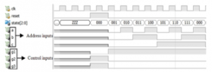
Figure 9: Test Pattern Generation for 3 : 8 Decoder (74HC138 IC)
Table 5: Power consumption in real time testing
| Power Values during testing (Real time condition) | ||||
| Sl.No | Module Name | Powered on state (No code) | Running State (With code) | Designed module Power |
| 1 | Final code | 0.25Ax5V = 1.25W | 0.30Ax5V = 1.50W | (Running code ) – (Powered on condition) = 1.50 – 1.25 = 0.25W |
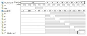
Figure 10: Latching of IC outputs is verified through testbench
Propagation Delay test concept is verified through simulation results as shown in Figure 11. The signal ‘edge_det2’ shows rising edge of input test vector and signal ‘edge_det5’ shows rising edge of IC output. The ‘count time’ register gives the number of counts between the change in the input and output of DUT. The number of clocks marked in the waveform is matched with value stored in the ‘count time ’register. This logic is verified through hardware and found the count time value for each IC to be tested. This count time value is multiplied with clock period to get the propagation delay as mentioned in Table 3.

Figure 11: Finding the time between change of input to change of output
5.1. Implementation Results
- Dual IC Testing (DIP and SOIC Package)
Dual IC testing presented in paper [1], the Decoder (74138-SOIC) and XOR (7486-DIP) ICs were tested simultaneously. The 7486 – XOR IC was tested by applying all possible test vectors to each gate simultaneously and latched outputs were compared with desired values. ‘P’ on the seven-segment display represents result status of the individual gate in IC. Figure 12 shows Dual IC testing setup. Results of both ICs were verified through LEDs.

Figure 12: Results of Dual IC tesing (74HC138 and 7486 ICs)
- Quad IC testing (TSSOP,SOIC,DIP,DIP- Package)
In Quad IC testing, Buffer – 74HC244 (TSSOP), Decoder – 74HC138 (SOIC), Dual 4:1 MUX – 74HC153 (DIP), XOR Gate – 74HC86 (DIP) ICs with various packages are tested simultaneously. The Figure 13 shows the results of Buffer IC among four ICs. ‘IC1P’ on the seven segment display represents result status of particular IC as free of error. Buffer IC is tested with fast mode, one time execution method and results shown on LEDs are last combination of test vector i.e. 0x55. IC selection should be set to ‘001’ to monitor Buffer IC result. Similarly, decoder IC also tested in fast and one time execution mode. Both multiplexers in dual 4:1 MUX IC and quad gates in XOR IC are tested at same time. All ICs results are monitored through LEDs by setting switches. Quad IC testing is verified simultaneously without modifying source code.
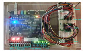
Figure 13: Buffer IC (74HC244) result during Quad IC Testing
The comparison is made between FPGA based Quad-IC tester and available IC testers in market and it is shown in Table 6. The Quad IC tester is having all existing features like multi package support, loop test capability, truth table verification etc. except unknown IC identification. With additional to these features, the Quad IC tester has capability of testing four ICs at a time (parallel execution) with more speed. Throughput calculation is made for single IC and Quad IC testing by using equation (3). The comparison results are demonstrated in the Figure 14 with respect to number of ICs tested per hour. The speed of proposed IC tester is about 0.01sec, which is much lower than speed of existing IC tester i.e. 0.8 sec. Also, Quad IC tester has some more features like Propagation delay and operating frequency range test. The Altera FPGA Cyclone II EP2C20F484C7 device’s (Now its Intel) utilization summary for quad IC testing logic is given in the Figure 15. Implementation of quad IC testing has utilized about 1% of logic and 32% of I/O pins of cyclone II device. So, to provide highly extended support still lot of ICs can be included into tester.

Figure 14: Throughput comparison between Single IC and Quad IC Testing
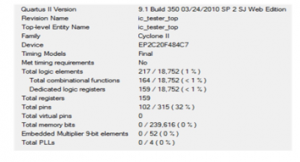
Figure 15: Device Utilization summary for Quad IC Testing
6. Conclusion
In this paper, portable Quad-Site Tester for digital ICs is implemented with automatic testing approach on FPGA. Testing has been carried out on Quad ICs simultaneously with features such as Propagation Delay and Operating frequency test along with Functional test. The concurrent testing with true parallel execution is the main key of proposed IC tester which greatly reduce the test time and cost compared with traditional testing. The proposed Quad IC tester improves throughput by 11% compared with existing IC testers. In this context, considering index time as 7secs as it is done by manually and testing time is 1sec. If index time becomes less than the execution time, then there will be significant change in throughput. This can be achieved by automatic replacing of ICs using hardware setup.
Also, throughput can be further increased by enhancing the work to Octal-Site testing. The proposed IC tester consumes 70% less power compared to existing IC testers.
In future, proposed work can be enhanced to include analog ICs (ADC, DAC, Opamps, and Analog MUX etc.), peripheral ICs (UART, level translators, drivers etc.) and memories with support of different packages like Thin Small Outline Package (TSOP), Thin Quad Flat Package (TQFP), and Plastic Leaded Chip Carrier (PLCC) etc.
Table 6: Comparison with existing testers
| Features | IC Tester (Outside INDIA) | IC Tester (INDIA) | FPGA based Proposed Tester |
| Quad IC testing (Different type) | No | No | Yes |
| Package Support | DIP/SOIC | DIP | DIP/SOIC/TSSOP |
| Parallel Execution | No | No | Yes |
| Propagation Delay Test | No | No | Yes |
| Testing Speed | 0.8sec | Not shown | 0.01sec |
| Power Consumption | 5W | 6W | 2W |
| MC/FPGA based | MC based | MC based | FPGA based |
| Battery operated | Yes | Yes | Can be incorporated in the system |
| Loop-test capability | Yes | Yes | Yes |
| Truth table observation | No | Yes | Yes |
| Counting process observation | No | Yes | Yes |
| Unknown IC identification | Yes | Yes | Can be enhanced to this feature as proposed IC tester is reconfigurable |
Conflict of Interest
The authors declare no conflict of interest.
- B. Rabakavi, Saroja Siddamal, “Design of High Speed, Reconfigurable Multiple ICs Tester using FPGA Platform”, IEEE, ICEECCOT, 909-914, December, 2018. https://doi.org/10.1109/ICEECCOT43722.2018.9001588.
- M. S. Zaghloul and M. Saleh, “Implementation of FPGA for decision making in portable automatic testing systems for ICs library & Digital Circuits ,” IEEE Applied Imagery Pattern Recongnition Workshop, 2011. https://doi.org/10.1109/AIPR.2011.6176361.
- B. Vermeulen, Camelia Hora, Bram Kruseman, Erik Jan Marinissen, Robert van Rijsinge, “Trends in Testing Integrated Circuits”, International Test Conference, IEEE, 2004. https://doi.org/ 10.1109/TEST.2004.1387330.
- I.A. Grout , Integrated Circuit Test Engineering: Modern Techniques, Springer, 2006.
- M.L. Bushnell, Vishwani D. Agrawal, Essentials of Electronic Testing for Digital, Memory and Mixed-Signal VLSI Circuits, Kluwer Academic Publishers, 2002.
- S. Fransi, G. L. Farré, L. G. Deiros, and S. B. Manich, “Design and Implementation of Automatic Test Equipment IP Module”, ETSYM, 2010. https://doi.org/ 10.1109/ETSYM.2010.5512749.
- L. Mostardini, L. Bacciarelli, L. Fanucci, L. Bertini, M. Tonarelli, and M. De Marinis, “FPGA Based Low Cost Automatic Test Equipment for Digital Integrated Circuits”, IEEE International Workshop on Intelligent Data Acquisition and Advanced Computing Systems: Technology and Applications, 21-23 September 2009.https://doi.org/ 10.1109/IDAACS.2009.5343031.
- A. A. Bayrakci, “ELATE: Embedded low cost automatic test equipment for FPGA based testing of digital circuits”, 2017 10th International Conference on Electrical and Electronics Engineering (ELECO), Bursa, 2017, pp. 1281-1285.
- H. Kim, Yong Lee, Sungho Kang, “A Novel Massively Parallel Testing Method Using Multi-Root for High Reliability”, IEEE Transactions on Reliability, 64(1), March 2015.https://doi.org/10.1109/TR.2014.2336395.
- T. Nakajima, Takeshi Yaguchi, Hajime Sugimura, “An ATE Architecture for Implementing Very High Efficiency Concurrent Testing”, International Test Conference, IEEE, 2012. https://doi.org/ 10.1109/TEST.2012.6401551.
- Gary L. West, H. Troy Nagle, Jr., Victor P. Nelson, “A Microcomputer-Controlled Testing System for Digital Integrated Circuits”, IEEE Transactions on Industrial Electronics and Control Instrumentation, IECI-27, No. 4, Nov. 1980.https://doi.org/10.1109/TIECI.1980.351644.
- J. Dunbar, “FPGA Based Design for Accelerated Fault-testing of Integrated Circuits” , Master’s Theses, Bucknell University, 2010.
- A. L. Boudreault, “Automatic Test Equipment in the Production Process”, IEEE Transactions on Manufacturing Technology, Volume-4, No.2, December 1975.https://doi.org/10.1109/TMFT.1975.1135861.
- Takashi Kitagaki, “Flexible ATE Module with Reconfigurable Circuit and Its Application”, International Test Conference, IEEE, 1999.https://doi.org/10.1109/TEST.1999.805826.
- J. Romoth, M. Porrmann, and U. Ruckert “ Survey of FPGA Applications in the period 2000-2015”, Center of Excellence Cognitive Interaction Technology, Bielefeld University, Germany. https://doi.org/10.13140/RG.2.2.16364.56960.
- S. S. Tripaliya and P. P. Bansod, “FPGA based IC Tester,” IJEEDC, ISSN: 2320-2084 , 3(5), May-2015.https://doi.org/10.1109/ITC-Asia.2019.00018.
- N. Velamati, Robert Daasch, “Analytical Model for Multi-site Efficiency with Parallel to Serial Test Times, Yield and Clustering”, 27th IEEE VLSI Test Symposium, 2009.https:doi.org/10.1109/VTS.2009.42.
- Y. Lee, Inhyuk Choi, Kang-Hoon Oh, James Jinsoo Ko and Sungho Kang, “Test Item Priority Estimation for High Parallel Test Efficiency under ATE Debug Time Constraints”, Teradyne inc. 2017. https://doi.org/10.1109/ITC-ASIA.2017.8097131.
- S. Kumar Goel, Erik Jan Marinissen, “On-Chip Test Infrastructure Design for Optimal Multi-Site Testing of System Chips” , Proceedings of the Design, Automation and Test in Europe Conference and Exhibition, 2005. https://doi.org/10.1109/DATE.2005.231.
- K. Voon Ching, “A Case Study of Return on Investment for Multi-sites Test Handler in The Semiconductor Industry Through Theory of Industry 4.0 ROI Relativity”, International Journal of Recent Contributions from Engineering, Science &IT, 7(3), 23-40, July 2019. https://doi.org/10.3991/ijes.v7i3.11057.
- Y. Takahashi, Akinori Maeda, “Multi Domain Test: Novel Test Strategy to reduce the Cost of Test”, 2011 29th IEEE VLSI Test Symposium, 2011. https://doi.org/10.1109/VTS.2011.5783738.