Shape Optimization of Planar Inductors for RF Circuits using a Metaheuristic Technique based on Evolutionary Approach
Volume 5, Issue 5, Page No 426-433, 2020
Author’s Name: Imad El Hajjami1,a), Bachir Benhala1, Hamid Bouyghf2
View Affiliations
1Faculty of Sciences, Moulay Ismail University, Meknes, 50050, Morocco
2FSTM Mohammedia, Hassan II University, Casablanca, 20000, Morocco
a)Author to whom correspondence should be addressed. E-mail: i.elhajjami@edu.umi.ac.ma
Adv. Sci. Technol. Eng. Syst. J. 5(5), 426-433 (2020); ![]() DOI: 10.25046/aj050553
DOI: 10.25046/aj050553
Keywords: Optimization, Integrated Inductors, Evolutionary Algorithms, Quality Factor, RF Circuits

Export Citations
In this article, we concentrate on the use of a metaheuristic technique based on an Evolutionary Algorithm (EA) for determining the optimal geometrical parameters of spiral inductors for RF circuits. For this purpose, we have opted for an optimization procedure through an enhanced Differential Evolution (DE) algorithm. The proposed tool allows the design of optimized integrated inductors not only with a maximum quality factor(Q), but also with a maximum self-resonant frequency (SRF), and a minimum surface area, in addition to being adapted to any model of any technology. This paper presents also a comparison between performances of the optimized inductors (inductor square shape and inductor circular shape), in terms of the quality factor, SRF, and circuit size. For the purpose of mitigating the impact of parasitic effects, design basics have been taken into consideration. Then, in order to investigate the efficacy of evaluated results, an (EM) simulator has been employed.
Received: 14 July 2020, Accepted: 08 September 2020, Published Online: 21 September 2020
1. Introduction
Integrated Inductors are of paramount importance elements, layout-optimization for spiral inductors has been the focus issue of several studies for the last few years, as for application, the four main characteristics that are required for the design of spiral inductors are: high inductance, high current capability, energy density, and low losses, with the inductors properties being identified by its geometrical and technological parameters [1].
For the sizing of spiral inductors, the designer should consider three main parameters [2], [3], the inductance value which is one of the most sensitive parameters, then, the quality factor (Q), and finally the self-resonant frequency (SRF).
Many works have been conducted for the sake of modeling and optimizing of spiral inductors. Formulation, modeling, and implementation remain the main steps for designing an integrated inductor [4], [5]. However, to ameliorate the optimization, the operation could be repeated many times till an acceptable solution is found.
Metaheuristic’s techniques are especially applied to the optimal sizing of analog circuits [6], such techniques have proven to be efficient in solving difficult problems because they necessitate less time to converge and yield better solutions.
In this field, the methods mostly used are EA: ‘Evolutionary Algorithms ’ [7], such as the Differential Evolution (DE) Algorithm [8], and the Genetic Algorithm (GE) [9], [10], but in the last two decades, a new group of nature-inspired heuristic optimization algorithms have been introduced as SI: ‘Swarm Intelligence Techniques’, such as Ant Colony Optimization (ACO) [11], [12], Gravitational Search Algorithm (GSA) [13], Artificial Bee Colony (ABC) [14], Dragonfly Algorithm (DA) [15], Particle Swarm Optimization (PSO) [16], Grey Wolf Optimizer (GWO) [17], and Bacterial Foraging Optimization (BFO) [18].
Nevertheless, for the sake of achieving the optimal sizing of the (RF) spiral inductors, the Differential Evolution (DE) is to be the focus technique in this paper since it has been widely used in circuit design in the last decade.
In order to design circular and square spiral inductors for operating frequencies around 2.5 GHz, the inductor π-model has been embedded in the improvement device.
The next sections of the paper layout introduce as follows: Section 2 is devoted to the descriptions of the inductor π-model used, afterward, section 3 provides the synopsis of the DE
algorithm, while the optimal values of DE parameters have been determined by a proposed technique. Then, section 4 highlights the inductor sizing-optimization method, the technological parameters, and the design constraints as well, besides, the optimization results are presented, where analytical results obtained with DE are investigated by ADS momentum simulation software. Last and not least, the conclusion is offered in section 5.
2. Planar Spiral Inductors
All the shapes of spiral inductor known by four main geometrical parameters, the spacing between lines (s), the number of turns (n), the line width (w), and the outer length of a side (dout), while the inner length of a side (din) defined by: din = (dout – 2.(n .(s + w) – s)).
There are other important geometry parameters such the inductor length, while: L = 4.n.davg for the square shape, and L = 4.n.davg for the circular shape, then, the inductor area: A=dout2, and finally, the average diameter: davg = 0.5.(dout + din).
Layouts of the circular and the square inductor have been showing respectively in Figure 1 and Figure 2 [19].
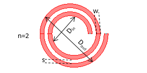
Figure 1: Layout of the Circular Integrated Inductor
2.1. The electrical Model of Integrated Inductors
It is important, thus, to present the expressions of the electrical model components for the inductor π-model, Figure 3 presented the electrical circuit for this type, while, Cs, Csi, Cox, Rs, and Rsi are respectively the substrate capacitance, the series capacitance between the spiral and the metal underpass, the substrate-oxide capacitance, the series resistance, and the substrate resistance, these parameters are determined by equations (1 2,3,4,5,6,7,8, 9):
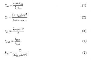
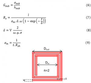
Figure 2: Layout of the Square Integrated Inductor
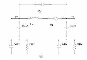
Figure 3: Integrated Inductor Electrical π -Model
where (t) is the turn thickness, (tox) is the oxide thickness between the spiral and the substrate, (σm) is the conductivity of the metal, (ω) is the frequency, (tox, M1-M2) is the oxide thickness between the spiral and the under-pass, (εox) is the oxide permittivity, (Gsub) is the substrate conductance per unit area, (Csub) is the substrate capacitance per unit area, (hsub) is the substrate height, (σsub) is the substrate conductivity, (δ) is the skin depth, (µ) is the magnetic permeability of free space, and finally, (Rsh) is the sheet resistance.
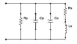
Figure 4: The Parallel π-Equivalent Circuit of Integrated Inductors
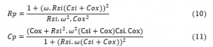
A similar inductor model has been shown in Figure 4, the quality factor (Q) was calculated by equations (10) and (11), where (Cp) is the shunt capacitance, and (Rp) is the shunt resistance.
2.2. Inductance Ls
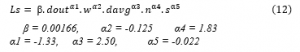
The model of the inductance Ls for the square inductor is expressed [19], [20] in equation (12):
The expression of the inductance Ls for the circular inductor is given in equation (13) [21]:
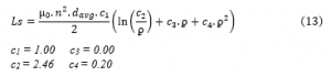
The coefficients ci, β, and αi are not depending on the technology but on the structure of the inductor. With ϼ is the fill ratio, inductances in nH, and dimensions in μm.
The expression of the inductance for a given frequency (f) for two ports [20] defined as follow:
2.3. The Quality factor (Q)
The quality factor is presented as follows:
An ideal inductor has an infinite Quality factor [19].
When the peak magnetic energy is the same as the electric energy, the Q-Factor is equal to zero, this phenomenon is defined as the self-resonant frequency phenomena.
The energy stockpiled in the inductor is attached to the imaginary part of the input admittance (Yin), whereas the real part of (Yin) is proportional to the energy dissipated in resistances, with this approach is abridged to [20]:
![]()
3. The Differential Evolution Algorithm
It is possible to say that the DE algorithm, as is the genetic algorithm, is a population-based using identical operators’ mutation, crossover, and selection. However; what makes the genetic algorithms yield a better solution is the fact that it builds on the crossover operation while the DE builds on the mutation one [8].
At the beginning of the DE process, the population of the n-pop solution vectors is randomly selected. This population is then ameliorated by stratifying mutation, crossover, and selection operators. First, the algorithm uses the mutation process as its search mechanism. Then, the DE uses crossover (recombination) operators, and the child vector that takes parameters from one parent more than the other. Afterward, a selection process is carried out in order to change the parent vectors if their fitness is less than of the newly generated child vectors. This three-stage process is repeated until a better solution is found [22].
The principal steps of the DE algorithm are defined mathematically as follows:
3.1. Mutation
For each objective vector xj, k ,a mutant vector is generated by (18):
![]()
where ?, ?1, ?2, ?3 ∈ {1, 2,…, ??} are arbitrary chosen and must be different from each other. In equation (18), (β) is the scaling factor which affects the difference vector .
3.2. Crossover
The trial vector is produced by the mixture of the parent vector with the mutated vector:
![]()
where (Pc) is the crossover probability parameter.
3.3. Selection
The comparison between a parent and its identical offspring called the selection and can be expressed as:
![]()
where g(x) is the objective function value of the trial vector. The DE algorithm can be declared in 1:
3.4. The DE Algorithm Parametrization
To determine the optimal values of DE parameters, the Ackley function presented in equation (21) was investigated for 100 population and 1000 number of iterations.
| Algorithm 1: Differential Evolution Algorithm | ||||
| Begin | ||||
| T=0; | ||||
| Generate the initial population of individuals N; | ||||
| Evaluate g (xj, k) | ||||
| For each individual i in the population do | ||||
| Choose r1, r2, r3 within the range [1, N] randomly; | ||||
| For each parameter j do | ||||
| Generate the mutant vector with equation (18) ; | ||||
| Generate a new vector with equation (19); | ||||
| end for | ||||
| if g (uj, k+1) ≤g (xj, k) then | ||||
| xj,k+1= uj,k+1 | ||||
| else | ||||
| xj,k+1= xj,k | ||||
| end if | ||||
| end for | ||||
| T=T+1; | ||||
| end | ||||
The Ackley function has one global minimum at: f ( xj ) = 0; for xj = ( 0 , … , 0 ).
The function evaluated on xj ∈ [ − 32, 32] for all (j = 1 , … , 32) .
Figure 5 displays the variation of fitness convergence according to the crossover probability Pc and the upper bound of the scaling factor betamax (with the lower bound of the scaling factor-beta min equal to 0,1). The cost function versus the number of iterations presented in Figure 6.
From Figure 5, the values of DE parameters that gave the best convergence are presented in Table 1.
4. Inductors Sizing
In the following section, we aim to maximize the Q-Factor for a specific value of the inductance for two structures, square and circular, by combining the inductor π-model and the DE optimization procedure. Afterward, simulations with ADSEM are adopted.
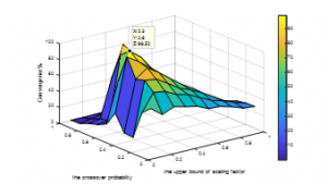
Figure 5: Convergence Rate versus the Crossover Probability and the Upper Bound of the Scaling Factor, with betamin=0.1.
4.1. Constraints of the study
To minify the parasitic phenomena [20], [23], the liaison between geometry parameters in (22) is well respected as a sort of included design-rules [20], [23].
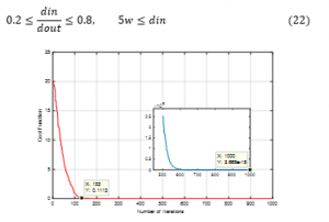
Figure 6: The Cost Function versus the Number of Iterations for the Ackley Function.
Table 1: Parameters Values of the Differential Evolution Algorithm.
| Parameter | Value |
| The crossover probability | 0.6 |
| The lower bound of the scaling factor | 0.1 |
| The upper bound of the scaling factor | 0.3 |
| Population size | 100 |
| The number of iterations | 500 |
- The SRF Constraint
The condition for a minimum self-resonant frequency which SRF SRFmin can be formed as [20]:
4.2. Optimization Procedure
The goal of this optimization is to find the optimum geometrical parameters of the spiral inductor to get a higher value of Q-Factor, the problem can be formulated as follows:
The objective function for the DE was defined as the following:
where (si) is the penalty coefficient, and P(x) is the sum of constraints.
Constraints g8(x), g9(x), g10(x), and g11(x) are boundary constraints, as result, they can be examined, while the DE was not allowed to generate a candidate vector farther these limitations.
Equations of constraints g4(x), g5(x), g6(x), and g7(x) have been shown in Table 2.
4.3. Results and Discussions
In the following, we will be adopting a sizing of square and circular inductors, with distinct values of the inductance Lsreq in the field beyond 2.5 GHz, as shown in Table 3 the technological and physical parameters have been well presented, while Table 4 represents the geometry parameter boundaries.
The details of the optimization have been presented in Table 5 and Table 6. On aim to verify our procedure, Figure 7 gives the cost function versus the number of iterations for square inductors, in this case, the constraint for minimum self– resonant frequency is added as SRFmin=22 GHz. The optimization results of the maximum Q-Factor and area (A) for both circular and square inductors versus the inductance obtained using the DE algorithm are presented in Figure 8.
The Q-Factor versus frequency for each value of the inductance has been shown in Figure 9 and Figure 10. The simulation using momentum software has also been shown in Figure 11, Figure 12, Figure 13, and Figure 14.
The comparison between optimization results and simulations is presented in Table 7 and Table 8.
Table 2: Equations of Constraints.
| Constraint | Equation |
| g4(x) | (Din/Dout)-0.8 |
| g5(x) | 0.2-(Din/Dout) |
| g6(x) | (2.n+1).(s+w)-Dout |
| g7(x) | (5.w-Din) |
Table 3: The values of technological parameters.
| Symbol | Parameter | Value |
| t | Metal thickness | 2.8 μm |
| s | Metal conductivity | 4 ´ 107 Ω/m |
| ϼ | Substrate resistivity | 0.2 Ω.m |
| tsub | Substrate thickness | 600 μm |
| tox | The thickness of the oxide | 6.42 μm |
| εr | The relative permittivity of the silicon | 11,9 |
| m | The magnetic permeability of free space | 4p ´ 10–7 H/m
|
| tox_m1-m2 | Oxide thickness between spiral and underpass | 0.66 μm |
| εr | The relative permittivity of the Oxide | 4 |
| ε0 | Permittivity of vacuum | 8.85 ´ 10–12 F/m |
Table 4: Sizing Variables and their Allowable Ranges.
| Sizing variable | Lower bound | Upper bound |
| w | 1 μm | 12 μm |
| dout | 140 μm | 280 μm |
| s | 2 μm | 2.5 μm |
| n | 1.50 | 12.00 |
Table 5: Optimization Results of Circular Inductors using the DE Algorithm.
| Lsreq | LsAn | Dout | w | s | n | Q |
| 1.00 | 1.00 | 166.12 | 12.00 | 2.38 | 3.50 | 8.26 |
| 3.00 | 3.00 | 220.00 | 12.00 | 2.32 | 5.50 | 11.44 |
| 5.00 | 5.00 | 238.85 | 11.30 | 2.03 | 7.00 | 12.91 |
| 7.00 | 7.00 | 261.11 | 11.10 | 2.00 | 8.00 | 13.34 |
| 9.00 | 9.00 | 268.03 | 10.13 | 2.00 | 9.00 | 12.90 |
| 11.00 | 11.00 | 265.34 | 8.81 | 2.00 | 10.00 | 12.16 |
| 13.00 | 13.00 | 280.00 | 8.60 | 2.00 | 10.50 | 11.57 |
| 15.00 | 15.00 | 273.35 | 7.66 | 2.00 | 11.50 | 11.13 |
Table 6: Optimization Results of Square Inductors using the DE Algorithm.
| Lsreq | LsAn | Dout | w | s | n | Q |
| 1.00 | 1.05 | 140.00 | 12.00 | 2.00 | 2.50 | 9.74 |
| 3.00 | 2.97 | 201.00 | 11.99 | 2.00 | 3.50 | 13.13 |
| 5.00 | 4.99 | 230.00 | 10.14 | 2.00 | 4.00 | 13.22 |
| 7.00 | 7.00 | 240.00 | 8.37 | 2.00 | 4.50 | 12.48 |
| 9.00 | 9.00 | 250.20 | 7.69 | 2.00 | 5.00 | 12.28 |
| 11.00 | 11.00 | 260.00 | 7.45 | 2.00 | 5.50 | 12.21 |
| 13.00 | 13.00 | 267.00 | 7.24 | 2.00 | 6.00 | 12.01 |
| 15.00 | 15.00 | 272.00 | 7.01 | 2.00 | 6.50 | 11.69 |
Figure 7: The Objective Function versus Iterations Number for a Square Inductor.
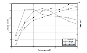
Figure 8: The Quality Factor and Inductors Area versus Inductance.
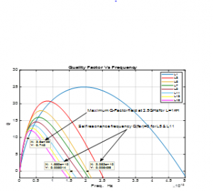
Figure 9: The Quality Factor of Square Inductors versus Frequency.
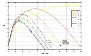
Figure 10: The Quality Factor of Circular Inductors versus Frequency.
What the results show is that when the inductance value increases, the quality factor decreases, and the self-resonant frequency decreases as well.
However, the results are very good in terms of the circuit’s size, and the constraints are very robust.
The DE algorithm provides better results concerning the circuit’s size and has a faster convergence as shown in the results.
We can notice that the simulation of square inductors is very accurate, with an error below 8.50% for the inductance value, and 5.21% for the quality factor for Ls less than 11 nH. It is possible to explain the increase of the error when the value of inductance is greater than 11 nH, in that we have taken similar limits of geometrical parameters for all values of the inductance, when the value of Ls has augmented, the number of turns became higher and Dout increased with a small percentage, in such
circumstances, the quality factor decreases owing to the parasitic phenomena effects, this problem can be solved by increasing the parameters of the allowable range in the proportion of the outer diameter.
As for the circular inductor, generally, the error is below than 5.66% for inductance value, and 21.56% for the quality factor, Although, this type has the shortest perimeter, and with a circular configuration, a higher quality factor (Q) is obtained. Yet, this type shows a response to the parasitic phenomena effects.
We notice through the simulation that the circular inductor is not significantly affected by parasitic phenomena in terms of the self-resonant frequency. From Figures 10 and 13, we observe that the inductor of Ls equal to 11 nH reaches its maximum of Q-Factor when fmax ~ 2 GHz, the area on the left of fmax, is an area where the Q-Factor is fundamentally affected by the magnetic induced losses, skin and proximity effects, and the DC resistance [24],[25]. On the opposite side of fmax, in addition to the preceding effects, the Q-Factor is also affected by the substrate noise coupling [23]. The evaluated SRF equal to 10.1 GHz, and the SRF obtained via simulation equal to 8.5 GHz, at this time, the Q-Factor is equal to 0, starting from this point, the peak magnetic energy is less than the electric energy, due to the perturbation of this last because of the parasitic phenomena.
The layout constraints for circular inductors required extensive research, in order to mitigate the parasitic phenomena effects.
Moreover, the degradation of the Q-Factor can be seen more clearly for square inductors, from Figures 9 and 11, for Ls equal to 11 nH, the Q-Factor equal to 0 when the evaluated SRF equal to 15.59 GHz and the SRF obtained via simulation equal to 7 GHz, we conclude that this type is extremely influenced by the parasitic phenomena.
Table 7: Comparison between Optimization Results and Momentum Simulations for Circular Inductors.
| LsAn | LsEM | ϵ% | QAN | QEM | ϵ% |
| 1.00 | 1.25 | 25.00 | 8.26 | 9.20 | 11.80 |
| 3.00 | 2.96 | 1.33 | 11.44 | 10.82 | 5.41 |
| 5.00 | 4.81 | 3.80 | 12.91 | 11.34 | 12.16 |
| 7.00 | 6.72 | 4.00 | 13.34 | 10.94 | 16.50 |
| 9.00 | 8.49 | 5.66 | 12.90 | 11.29 | 12.48 |
| 11.00 | 11.32 | 2.90 | 12.16 | 9.86 | 18.91 |
| 13.00 | 13.28 | 2.15 | 11.57 | 9.40 | 18.75 |
| 15.00 | 15.35 | 2.33 | 11.13 | 8.73 | 21.56 |
Table 8: Comparison between Optimization Results and Momentum Simulations for Square Inductors.
| LsAn | LsEM | ϵ% | QAN | QEM | ϵ% |
| 1.05 | 0.96 | 8.50 | 9.74 | 10.09 | 3.59 |
| 2.97 | 2.78 | 6.39 | 13.13 | 13.65 | 3.96 |
| 4.99 | 4.74 | 5.01 | 13.22 | 13.66 | 3.32 |
| 7.00 | 6.78 | 0.80 | 12.48 | 13.97 | 4.25 |
| 9.00 | 8.72 | 3.14 | 12.28 | 13.12 | 5.21 |
| 11.00 | 10.79 | 1.90 | 12.21 | 12.15 | 0.49 |
| 13.00 | 12.74 | 2.00 | 12.01 | 10.81 | 10.00 |
| 15.00 | 14.85 | 1.00 | 11.69 | 9.67 | 17.27 |
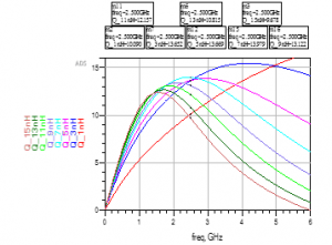
Figure 11: Simulation of the Quality Factor versus Frequency in Momentum for Square Inductors.
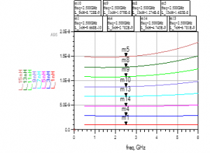
Figure 12: Simulation of the Inductance versus Frequency in Momentum for Square Inductors.
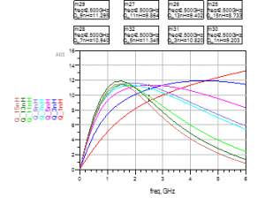
Figure 13: Simulation of the Quality Factor versus Frequency in Momentum for Circular Inductors.
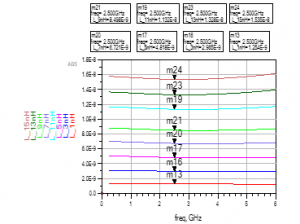
Figure 14: Simulation of the Inductance versus Frequency in Momentum for Circular Inductors.
5. Conclusion
For dealing with the optimal sizing of spiral inductors for (RF) circuits, we proposed on this paper an application of the Differential Evolution (DE) algorithm. Two inductor structures have been optimized i.e. shape square and shape circular, with a maximum Q-Factor, a maximum self-resonant frequency (SRF), and a minimum surface area. The performances of optimized inductors showed good results in terms of the Q-Factor, with the square inductor presenting a higher SRF and a smaller area (A) than the circular one.
The π-model does not allow for the assimilation of noises parasitic effects in a good way, leading to a lower SRF value, that is why we are focusing on using the double π-model, instead, for the integrated inductors optimal sizing.
- J. M. Lopez-Villegas, J. Samitier, C. Cane, P. Losantos, J. Bausells, “Improvement of the quality factor of RF integrated inductors by layout optimization,” IEEE Transactions on Microwave Theory and Techniques, 48(1), 76–83, 2000, https://doi.org/10.1109/22.817474
- H. M. Hsu, K. Y. Chan, H. C. Chien, H. C. Kuan, “Analytical design algorithm of planar inductor layout in CMOS technology,” IEEE Transactions on Electron Devices, 55(11), 3208–3213, 2008, https://doi.org/10.1109/TED.2008.2004248
- J. N. Burghartz, B. Rejaei, “On the design of RF spiral inductors on silicon,” IEEE Transactions on Electron Devices, 50(3), 718–729, 2003, https://doi.org/10.1109/TED.2003.810474
- Y. Yorozu, M. Hirano, K. Oka, Y. Tagawa, “Improvement of the quality factor of RF integrated inductors by layout optimization,” IEEE Transactions on Microwave Theory and Techniques, 48(1), 76–83, 2000, https://doi.org/10.1109/22.817474
- S. Abi, H. Bouyghf, A. Raihani, B. Benhala, “Swarm intelligence optimization techniques for an optimal RF integrated spiral inductor design,” in 2018 International Conference on Electronics, Control, Optimization and Computer Science (ICECOCS), Kenitra, Morocco, 1–7, 2018, https://doi.org/10.1109/ICECOCS.2018.8610524
- P. Siarry, Z. Michalewicz, Advances in metaheuristics for hard optimization, Natural Computing Series, Springer, 2008.
- M. Crepinsek, S. H. Liu, M. Mernik, “Exploration and exploitation in evolutionary algorithms: A survey,” ACM Computing Surveys, 45(3), Article 35, 2013, https://doi.org/10.1145/2480741.2480752
- R. Storn, K. Price, “Differential evolution: A simple and efficient heuristic for global optimization over continuous spaces,” J. Global Optimization, 11(4), 341–359, 1997, https://doi.org/10.1023/A:1008202821328
- A. El Beqal, B. Benhala, I. Zorkani, “A Genetic algorithm for the optimal design of a multistage amplifier,” International Journal of Electrical and Computer Engineering, 10(1), 129–138, 2020, http://doi.org/10.11591/ijece.v10i1.pp129-138
- M. Mitchell, An introduction to genetic algorithms, The MIT Press, 1998.
- B. Benhala, “Sizing of an inverted current conveyors by an enhanced ant colony optimization technique,” in 2016 Conference on Design of Circuits and Integrated Systems (DCIS), Granada, Spain, 1–5, 2016, https://doi.org/10.1109/DCIS.2016.7845271
- L. Kritele, B. Benhala, I. Zorkani, “Ant Colony Optimization for Optimal Low-Pass Filter Sizing,” in: E. G. Talbi, A. Nakib. (Eds.), Bioinspired Heuristics for Optimization, Studies in Computational Intelligence, Springer, Cham, 283–299, 2019, https://doi.org/10.1007/978-3-319-95104-1_18
- E. Rashedi, H. Nezamabadi, S. Saryazdi, “GSA: A gravitational search algorithm,” Information Sciences, 179(13), 2232–2248, 2009, https://doi.org/10.1016/j.ins.2009.03.004
- C. J. Lin, M. L. Huang, “Modified artificial bee colony algorithm for scheduling optimization for printed circuit board production,” Journal of Manufacturing Systems, 44(1), 1–11, 2017, https://doi.org/10.1016/j.jmsy.2017.04.006
- S. Mirjalili, “Dragonfly algorithm: A new meta-heuristic optimization technique for solving single-objective, discrete, and multi-objective problems,” Neural Computing and Applications, 27(4), 1053–1073, 2016, https://doi.org/10.1007/s00521-015-1920-1
- B. Benhala, P. Pereira, A. Sallem, Focus on swarm intelligence research and applications, Nova Science Publishers, 2017.
- S. Mirjalili, S. M. Mirjalili, A. Lewis, “Grey wolf optimizer,” Advances in Engineering Software, 69, 46–61, 2014, https://doi.org/10.1016/j.advengsoft.2013.12.007
- K. M. Passino, “Biomimicry of bacterial foraging for distributed optimization and control,” IEEE control systems Magazine, 22(3), 52–67, 2002, https://doi.org/10.1109/MCS.2002.1004010
- C. P. Yue, C. Ryu, J. Lau, T. H. Lee, S. S. Wong, “A physical model for planar spiral inductors on silicon,” in International Electron Devices Meeting, Technical Digest, San Francisco, USA, 155–158, 1996, https://doi.org/10.1109/IEDM.1996.553144
- S. S. Mohan, M. del Mar Hershenson, S. P. Boyd, T. H. Lee, “Simple accurate expressions for planar spiral inductances,” IEEE Journal of Solid-State Circuits, 34(10), 1419–1424, 1999, https://doi.org/10.1109/4.792620
- B. Rejaei, J. L. Tauritz, P. Snoeij, “A predictive model for si-based circular spiral inductors,” in Topical Meeting on Silicon monolithic integrated circuits in RF systems, Ann Arbor, 148–154, 1998, https://doi.org/10.1109/SMIC.1998.750210
- D. Karaboga, B. Akay, “A comparative study of Artificial Bee Colony algorithm,” Applied Mathematics and Computation, 214(1), 108–132, 2009, https://doi.org/10.1016/j.amc.2009.03.090
- P. Pereira, M. H. S. Fino, F. V. Coito, M. V. Neves, “RF integrated inductor modeling and its application to optimization-based design,” Analog Integrated Circuits and Signal Processing, 73, 47–55, 2011, https://doi.org/10.1007/s10470-011-9682-x
- J. Aguilera, R.Berengue, Design and test of integrated inductors for RF applications, Dordrecht: Kluwer Academic Publishers, 2004.
- Y. Cao , R. A. Groves, X. Huang, N. D. Zamdmer, and al, “Frequency-independent equivalent-circuit model for on-chip spiral inductors,” IEEE Journal of Solid-State Circuits, 38(3), 419–426. 2003, https://doi.org/10.1109/JSSC.2002.808285
Citations by Dimensions
Citations by PlumX
Google Scholar
Scopus
Crossref Citations
- S. Akkader, H. Bouyghf, A. Baghdad, A. Kchairi Belbachir, M. El Bakkali, "Fabrication of compact substrate integrated waveguide dual band bandpass filter using complementary split-ring resonators for C and X band applications." e-Prime - Advances in Electrical Engineering, Electronics and Energy, vol. 9, no. , pp. 100739, 2024.
- Imad El Hajjami, Bachir Benhala, "Simulation Experiments of Different Metaheuristics Algorithms using Benchmark Functions: A Performance Study." In 2022 International Conference on Intelligent Systems and Computer Vision (ISCV), pp. 1, 2022.
- Halil Alpaslan, Erkan Yuce, Shahram Minaei, "A New Active Device Namely S-CCI and Its Applications: Simulated Floating Inductor and Quadrature Oscillators." IEEE Transactions on Circuits and Systems I: Regular Papers, vol. 69, no. 9, pp. 3554, 2022.
- Xiaobing Shen, Yu Zuo, Jiaze Kong, Wilmar Martinez, "Artificial Intelligence Applications in High-Frequency Magnetic Components Design for Power Electronics Systems: An Overview." IEEE Transactions on Power Electronics, vol. 39, no. 7, pp. 8478, 2024.
- Imad El hajjami, Bachir Benhala, Hamid Bouyghf, "Comparative Study between the Genetic Algorithm and the Artificial Bee Colony Technique: RF Circuits Application." In 2020 IEEE 2nd International Conference on Electronics, Control, Optimization and Computer Science (ICECOCS), pp. 1, 2020.
No. of Downloads Per Month
No. of Downloads Per Country