Design and Implementation of Reconfigurable Neuro-Inspired Computing Model on a FPGA

Adv. Sci. Technol. Eng. Syst. J. 5(5), 332–341 (2020);
 DOI: 10.25046/aj050541
In this paper we design a large scale reconfigurable digital bio-inspired computing model. We consider the reconfigurable and event driven parameters in the developed field-programmable neuromorphic computing system. The various Intellectual Property (IP) cores are developed for the modules such as Block RAM, Differential Clock, Floating Point, and First In First Out (FIFO) for the design of the neuron model in Xilinx ISE, with exploration of register transfer logic (RTL) and hardware synthesis using Verilog code. The architecture for design at device level offers the best possible design tradeoff for specific processor architectures and development choices. In this paper we perform algorithmic design of a large scale reconfigurable logical bio-inspired computing model. The proposed algorithm is implemented on Field Programmable Gate Array (FPGA) to develop a neuron model to be utilized in neuromorphic computing system.
1. Introduction
This research manuscript is an extension of work originally presented in International Conference on Artificial Intelligence and Signal Processing [1]. The bio-inspired computing is achieved with core building blocks of neuromorphic engineering which mainly constitute circuits and systems and is proposed as structures of spin devices [2].
The above direction opens a new path and induces a key approach for developing bio-inspired algorithms for implementations of bio-inspired algorithm based computing systems [3]. In nature the crucial role of learning and memory is achieved with help of synapses. The synapses which are plastic in nature, is formed with inter cellular connections of neurons, and the combination of these biological structures form the basic building blocks of neural networks [4]. Synapses can change their state based on the neural activity of coupled neurons. The functionality of neurons and synapses is mimicked in hardware by utilizing very large scale integration technology, plays a key role in design of neuromorphic computing systems [5]. The pathway to efficient neuromorphic systems is encoding the neural and synaptic functionalities in an electronic spin. It shows the potentials to exploit energy efficiency, performance, reliability, and magnetization using electric fields, and enhanced memory density of spintronic memory devices [6]. The bio-inspired computing systems is presented, with an aim to establish interaction framework, between two directions of natural system computation and artificial system computation [7]. In the in-memory computing for emerging memory devices, there is no separation between memory and logic, to overcome Von-Neumann bottleneck and also in-memory computing devices are designed with zero-off state power and due to this, they have a distinct advantage of the non-volatile state [8]. The in-memory computing is combined with a high gate or synapse density which enables forming of cross-bar array in the device, which can be easily integrated with CMOS with high density, operating with high current and voltage consuming high dynamic power, with In-memory computing device contains long switching time hence they operate with limited speed and have limited endurance, again the cross-bar in-memory computing is highly parallel, operate with low-power, low cost [9]. The verticals of Cross-bar in-memory computing are bio-inspired computing, deep learning, in-memory logic, chip/data security, architecture, device modeling [10]. The static random access memory latches and capacitors are utilized in a very large scale integrated devices, an architecture to implement strewed memory elements is embodied in this in-memory computing device as depicted in Figure 1 is aimed towards supporting the use of memristive devices as digital and synapse-like memory elements. The key contributions of the research manuscript are:
- Algorithmic design of a large scale reconfigurable logical bio-inspired computing model.
- Implementation of bio-inspired model on FPGA.
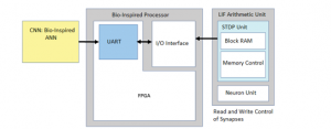
Figure 1: Block Diagram of FPGA based Bio-Inspired Computing System
2. Background
The emerging research architectures which support memory-based computing, exponential performance scaling, which enables mixed mode technology solutions. The problem of establishing the bridge between natural and artificial computation is one of motivation which illuminates the bio-inspired computation in artificial systems [11]. The paradox of programming a bio-inspired computer is the need to figure out the new class of algorithms, we are also missing out some very important basic concepts. The intelligent computational system are initially built with a Boolean logic or functions, next through logical phase, and into semiconductor technology phase, further into computational complexity phase and ends at an experimental computation phase [12]. The lesson learnt here is while dealing with intelligence the first stage is to probe into evolution, complexity, and also thermodynamics which is not an equivalent of a Boolean logic or functions, during the second stage new and novel electronics technology is required which is not an equivalent of electronics technology, which was defined during the computation phase, in the further stage the implementation complexity is not an equivalent to computational complexity, and the final stage is the practical intelligence stage which is also not an equivalent practical computation stage, defined during process of computation [13]. The factor synaptic plasticity, which accounts for the determination of the magnitude of the synaptic weights. The plasticity is also called as the learning of the synaptic junctions which probes the cognitive abilities to the bio-inspired architectures [14]. For analysis, if an experiment is performed considering the circuit with four access transistors to decouple read and write current paths, with the peripheral circuits for timing window, and aimed towards the spike-timing-dependent plasticity (STDP) implementation. Apart from these four transistors, one more transistor named as MSTDP is also connected to pre-charge line in the circuit, which is responsible to implement the STDP and this transistor is biased in the sub threshold saturation regime. The gate voltage of MSTDP transistor is called as PRE voltage, which starts increasing linearly as the pre neuron spikes [15]. As the post neuron is triggered, the POST signal is activated with the current flows through the device. The current is also known as the programming current , which is the 1 ns duration write current and is exponentially related with the magnitude to the delay factor of pre-neuron and post-neuron spikes. As the STDP measurements are taken between the % changes in the synaptic weights with respect to spike timing difference in (ms) , the synaptic weight is updated which depends on difference in the timing of post and pre neuron spikes[16].
3. Algorithm Design
In this section the design of algorithm is enumerated for a FPGA based large scale logical reconfigurable neuron model.
| Algorithm 1: Algorithm for FPGA Top Level Module | ||||||
| Result: Top Level module of IP Block | ||||||
| Model initialization; | ||||||
| while Apply Clock Signal do | ||||||
| Instantiate Clock Signal; | ||||||
| if FSM Instantiation then | ||||||
| Select RAM;
Select MATMUL |
||||||
| Else | ||||||
| Compute:
Communication Unit; Initialize UART; Initialize FIFO; |
||||||
| End
Emulate layer of network; Read Weight RAM; Load input RAM; Process data as perceptron; |
||||||
| End | ||||||
To realize the spiking neural functionalities by utilizing the leaky-integrate magnetization dynamics [17]. To enable the abstraction of the magnetic functions as stochastic spiking neurons, the parameter required is the thermal noise which is prevalent in nano-magnets at certain temperatures which are not equal to zero [18]. The reconfigurable neuron model consists of two units such as finite state machine unit (FSM) unit and communication unit. The Algorithm 1 illustrates the abstract view of the top level model hierarchy. The IP core module as described in Figure 2(a) emulates the layer of the network and loads data (weight or input) and then process the data to obtain the synapse weight output as depicted in Figure 2(b). Further the flag signal is controlled in
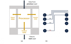
Figure 2: (a) IP-core module (b) Details of synapse weight information
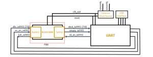
Figure 3: RTL schematic of Top Layer with sub-module Read/Write Memory
order to make the FSM to halt while the other sub programs are running [19]. The layer of the network is mimicked with reading the weight information from weight RAM, along with load input data from input RAM and processing the data as a simple neuron model [20]. The 8 bit parameter data width is applied as input to FPGA from data floating unit of USB module and from FPGA the parameter data is passed to FIFO block. The input data is further connected to din of input RAM, along with connecting row index to address of input RAM, and connection of read data to input of outgoing FIFO [21]. The outputs of last add operation is directly wired to the resultant RAM. The data packets are segmented at this stage and the information of data packets are available at the next stage. In the next stage the packet data is segmented into respective component registers. Write the input and weight data to padded variables when flag is high. The Figure 3 illustrates the above design process as sub-module read and write memory with FSM unit (with block RAM, Transmit FIFO, Receive FIFO) and universal asynchronous receiver and transmitter (UART) unit. Further also describes the communication link between FSM unit and the UART unit. Here the data sent from universal serial bus (USB) transforms to parallel data and is then sent to the FIFO for processing [22]. The Figure 3 can be considered as register transfer logic (RTL) schematic of the top layer module.
4. Implementation
In this section the implementation details of large scale reconfigurable digital bio-inspired computing model is described. The algorithm described is implemented on the hardware FPGA environment satisfying the requirement of hardware combined with the software co-design concept. The hardware used is FPGA ALTERA DE2 with a cyclone chip.
The Figure 4 represents the topology of the FSM of a RAM read/write process with FIFO pop data in sequence. The complete architecture of the bio-inspired computing system consists of system controller based on an advanced reduced instruction set computing (RISC) machine (ARM) processor, core-array of two dimensions, and a UART Controller. The interpretation of data is dependent of the order of popping the data. Sub-module MATMUL contains two dot product operations in parallel, which consists of floating point IPs as shown in Figure 5 in the form of
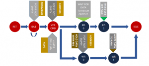
Figure 4: FSM Topology of Read/Write Process
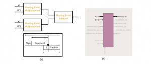
Figure 5: Submodule Dot Product Module/Process

Figure 6: Information Transfer Packet
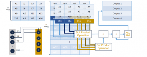
Figure 7: Implementation of a single core consists of 16 inputs and 4 outputs, implying that the weight RAM is 64 rows in depth.
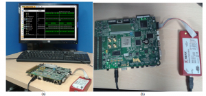
Figure 8: (a) The bio-inspired computing system setup (b) FPGA ALTERA DE2 Board setup with Xilinx JTAG adapter
The implementation of a single core consists of 16 inputs and 4 outputs, implying that the weight RAM is 64 rows in depth as described in Figure 7. The implementation of bio-inspired computing system is done on Altera Cyclone IV FPGA contained as a part of ALTERA DE2 Board. The VERILOG language was used to program the bio-inspired framework and compiled in Xilinx ISE platform with x86 64 bit CPU executing on Linux Ubuntu 16.04 operating system.
5. Results Obtained
In this section the results obtained with various Intellectual Property (IP) cores which are developed for the modules such as Block RAM, Differential Clock, Floating Point, and First In First Out (FIFO) for the design of the neuron model in Xilinx ISE, with exploration of register transfer logic (RTL) and hardware synthesis using Verilog code are presented.
The Figure 8(a) depicts the complete setup of bio-inspired computing system implementation and the Figure 8(b) represents JTAG adapter connection with FPGA ALTERA DE2 Board. The Figure 9 illustrates the behavioral simulation of developed reconfigurable bio-inspired computing is obtained in Xilinx ISE environment. We can look at output ram data out signal to double check if the data is correct in simulation. The execution is based on vector less activity propagation with peak memory and execution is carried out in Vivado-v-2014.2 FPGA has considerable static power consumption, but normally efficient power is measured as difference in idle state and real-time data processing for the machine.
The equation for obtaining the parameters is described in Equation (1).
% Synaptic Pruning = (Number of Neurons pruned) / (Size of Network x Accuracy x Energy) (1)
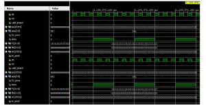
Figure 9: Behavioral simulation of the developed reconfigurable bio-inspired computing architecture
Table 1: Design Trade-off Parameters
| Parameters
[23], [24], [25] |
Existing Neuron Model | Proposed
Neuron Model |
Efficiency Improvement | Performance Improvement |
| 1. Computational Efficiency | 2.3 x Enhanced | 2 x Enhanced | 0.36 % | 89 % |
| 2. Energy efficiency | 2.8 x Enhanced | 3.2x Enhanced | – | High |
| 3. Throughput | High | High | – | – |
| 4. Accuracy | 90.02% | 90.4% | 1.69 % | 90 % |
| 5. Entropy | 10% – 25% for 800 Neurons | 12 % for 100 Neurons | – | 2 % |
On the other hand, a poor input output reflects the system glitch at which glue logic in FPGA DE2 board is affected in worst case, as the system changes the incoming events dynamically. The Table 1 depicts the architecture considerations for design at device level and offers the best possible design tradeoff for specific processor architectures and development choices. The parameters are described in Table 1 such as Computational Efficiency, Energy Consumption, Throughput, Accuracy, Entropy are compared with previous work with existing neuron model with the proposed neuron model. It is noteworthy that in the proposed design except LUT all other parameters have the same value for logic utilization post synthesis and post implementation, the reason behind this is the designed system is more of device specific. During Idle mode, the device does not process events and therefore there is no computation. The ADC14DS065/080/095/105 converts the analog data into 14 bit words, but it outputs the data on 1 or 2 serial data lines per channel. The digital output operates at LVCMOS voltage levels except for the serial signals and clock outputs LVDS signals.
These devices operate up to 65 million samples per second (MSPS) in a single lane mode while the higher data rates operate in a dual lane mode, each lane operates at half the data rate to keep the required clock frequencies from being excessive. Using this technique, the FPGA interface can support the highest data rate of 105 (MSPS) with a high throughput as shown in Table 1. The FPGA then will combine the two data streams appropriately to create the correct signals.
The serial data bus uses less board space for the signals, is easier to route and achieves similar data rates to a parallel interface with less wires for data bus. The parallel data bus from the ADC14155 can be connected to the FPGA using an I/O bank configured for 1.8 LVCMOS inputs. The data rate of this bus is 5-155 MHz, which is well within the I/O capabilities of the FPGA.
The designed FPGA module further consists of the blocks required for interfacing an ADC with the FPGA with 3.2x enhanced energy efficiency and 2x enhanced computational efficiency as described in Table 1.
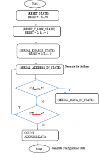
Figure 10: Flow diagram of the FPGA Response mechanism of developed reconfigurable bio-inspired computing architecture
The signals such as RESET and SEN indicate the reset state and serial enable state respectively of FPGA device selected. The serial register reset pulse is greater than 10 ns. If RESET=1; SEN=1 then the FPGA is in the reset state, if the signals RESET=0; SEN=1 then the FPGA is RESET_T_LOW_STATE, and if RESET = 0; SEN= 0, then the FPGA is in serial enable state. The Figure 10 illustrates the flow diagram which forms the basis for algorithm designed to implement a bio-inspired computing system. The A_COUNT is the address count for generating the address and D_COUNT is the data count to generate configuration data. To enable the serial interface of analog to digital converter (ADC), the serial registers were first reset to the default values and the RESET pin was kept low.
Serial enable (SEN), serial data (SDATA), and serial clock (SCLOCK) function as serial interface pins in this mode were used to access the internal registers of the ADC. The registers were reset either by applying a pulse on the RESET pin or by setting RESET bit high.
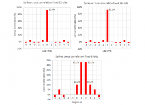
Figure 11: Spike Cross Correlation mechanism of developed reconfigurable bio-inspired computing architecture
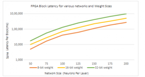
Figure 12: Rate of Change of BRAM generation in Cyclone-V FPGA Block Latency
For the increased flexibility, a combination of serial interface registers and parallel pin controls (CTRL1 to CTRL3) were used to configure the device. To enable this option, RESET pin was configured low. The parallel interface control pins CTRL1 to CTRL3 were available. After power up, the device is automatically configured according to the voltage settings on these pins. In the bus of ADC test for the CYCLONE-V FPGA device, the selected component bus is the 12 channel ADC_RAM component. The data captured through the single clock, the signals included are clock signals such as clk_p, clk_m, the reset signal and the 14 bit input and output data vector signals along with a data type register which is 14 bit vector. The timings of the spikes are analyzed, in a cross correlation of the spikes timings over the FPGA implementation. It is observed that 93% and 92% of the spikes are correlated in the 32 and 16-bits implementation respectively with the implementation with a zero lag delay. On the other hand, 8-bit implementation is slightly different, with 87% of the spike shifted between 0 and 3ms and centered in a 1.5ms shift average with entropy of ~12 % for 100 Neurons with ~2% of performance improvement as described in the Table 1. The analog to digital converter configuration through the serial mode with the signals as seen in spike cross correlation simulation result depicted in the Figure 11. The signals are clock, reset, serial clock, adc_ reset, serial data enable, serial data, and state of the system, the address data consists of a 16 bit vector and these parameters are calculated in terms of rate of change of Block-RAM generation in Cyclone-V FPGA as depicted in Figure 12 and with differential clock simulation time in FPGA based bio-inspired computing module is illustrated in Figure 13.
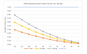
Figure 13: Differential Clock simulation time (in ms) for 1 ms real step in Cyclone-V
6. Conclusions
In this paper the FPGA based algorithmic design of a large scale reconfigurable logical bio-inspired computing model is carried out. The proposed algorithm is implemented on Field Programmable Gate Array to develop a neuron model to be utilized in neuromorphic computing system. The reconfigurable and event driven parameters are considered with the various Intellectual Property (IP) cores are developed for the modules such as Block RAM, Differential Clock, Floating Point, and First in First out (FIFO) for the design of the neuron model in Xilinx ISE, with exploration of register transfer logic (RTL) and hardware synthesis using Verilog code. The architecture for design at device level offers the best possible design tradeoff for specific processor architectures and development choices are summarized. This research paves a way for design of architecture that can be compatible for convolution neural network Artificial Neural Network (ANN).
Conflict of Interest
The authors declare no conflict of interest.
Acknowledgment
The Authors wish to thank School of ECE, REVA University, Bengaluru, India for providing necessary facilities in carrying out this research work.
- B.U.V. Prashanth, M.R. Ahmed, “FPGA Implementation of Bio-Inspired Computing Architecture Based on Simple Neuron Model,” 2020 International Conference on Artificial Intelligence and Signal Processing (AISP), 1–6, 2020, doi:10.1109/AISP48273.2020.9073420.
- B.U.V. Prashanth, M.R Ahmed, “FPGA Implementation of Bio-inspired Computing Based Deep Learning Model,” In Advances in Distributed Computing Machine Learning, Lecture Notes in Networks and Systems, 127. Springer, doi: 10.1007/978-981-15-4218-3_24.
- R.K. Sarma, M.T. Khan, R.A. Shaik, J. Hazarika, “A Novel Time-Shared and LUT-Less Pipelined Arch. for LMS Adapt. Filter,” IEEE Transactions on Very Large Scale Integration Systems, 28 (1), 188–197, 2020, doi:10.1109/TVLSI.2019.2935399.
- Mohammed Riyaz Ahmed B.K Sujatha, “Reinforcement Learning based on Computational Cognitive Neuroscience in Neuromorphic VLSI Chips,” International Journal of Advanced Research in Computer Science and Software Engineering, 2 (8), 2013.
- B.U.V. Prashanth, M.R. Ahmed, “Design and performance analysis of artificial neural network based artificial synapse for bio-inspired computing,” in Advances in Intelligent Systems and Computing, 1108, 2020, doi:10.1007/978-3-030-37218-7_135.
- C. Pan, A. Naeemi, “Beyond-CMOS non-Boolean logic benchmarking: Insights and future directions,” in Proceedings of the 2017 Design, Automation and Test in Europe, 2017, doi:10.23919/DATE.2017.7926971.
- X. Lou, Y.J. Yu, P.K. Meher, “Lower Bound Analysis and Perturbation of Critical Path for Area-Time Efficient Multiple Constant Multiplications,” IEEE Transactions on Computer-Aided Design of Integrated Circuits and Systems, 2017, doi:10.1109/TCAD.2016.2584181.
- A. Agarwal, L. Bopanna, “Low Latency Area-Efficient D.A Based Multi-Rate Filter Architecture for SDR Receivers,” Journal of Circuits, Systems and Computers, 27 (08), 2018, doi:10.1142/S0218126618501335.
- T. Xu, A. Fumagalli, R. Hui, “Efficient R.T Digital Subcarrier Cross-Connect (DSXC) Based on D.A DSP Algorithm,” in Journal of Lightwave Technology, 38(13), 3495-3505, 2020, doi: 10.1109/JLT.2019.2937787.
- D. Datta, P. Mitra, H.S. Dutta, “FPGA implementation of high performance digital down converter for SDR,” Microsystem Technologies, 2019, doi: 10.1007/s00542-019-04579-w.
- B.K. Mohanty, P.K. Meher, “An Efficient Parallel DA-Based Fixed-Width Design for Approximate Inner-Product Comp,” IEEE Transactions on Very Large Scale Integration (VLSI) Systems, 28 (5), 1221-1229, 2020, doi:10.1109/TVLSI.2020.2972772.
- M.R. Ahmed, B.K. Sujatha, “A review on methods, issues and challenges in neuromorphic engineering,” in 2015 International Conference on Communication and Signal Processing, ICCSP 2015, 2015, doi:10.1109/ICCSP.2015.7322626.
- M. D’arco, E. Napoli, E. Zacharelos, “Digital circuit for seamless resampling adc output streams,” Sensors (Switzerland), 20 (6), 2020, doi:10.3390/s20061619.
- H. Jiang, C. Liu, L. Liu, F. Lombardi, J. Han, “A review, classification, and comparative evaluation of approximate arithmetic circuits,” ACM Journal on Emerging Technologies in Computing Systems, 13 (4), 1–34 2017, doi: 10.1145/3094124.
- Md Zahangir Alom, et al., “A state-of-the-art survey on D.L architectures,” Electronics, 8 (3), 292, 2019, doi: 10.3390/electronics8030292
- S. Fukami, H. Ohno, “Magnetization switching schemes for nanoscale three-terminal spintronics devices,” Japanese Journal of Applied Physics, 56(8), 0802A1, 2017, doi:10.7567/JJAP.56.0802A1
- T. Jungwirth, et al., “The multi directions of antiferromagnetic spintronics,” Nature Physics, 14 (3), 200, 2018, doi:10.1038/s41567-018-0063-6
- C. D. Schuman, et al., “A programming framework for neuromorphic systems with emerging technologies,” 4th ACM International Conference on Nanoscale Comp. and Comm., ACM, 2017, doi: 10.1145/3109453.3123958
- G. Sanchez, et al., “A highly scalable parallel spike-based digital neuro architecture for high-order fir filters using LMS adaptive algorithm,” Neurocomputing, 330, 425-436, 2019, doi:10.1016/j.neucom.2018.10.029.
- M. Sharma, S.K. Singh, “New Tech. Peasant Multiplication for Efficient Signal Processing Applications”, Indonesian Journal of Elect. Engineering Comp Science, 8 (3), 726-729, 2017, doi: 10.11591/ijeecs.v8.i3.pp726-729.
- W. Zhao et al., “A division-free and variable-regularized LMS-based generalized side lobe canceller for adaptive beamforming and its efficient hardware realization,” IEEE Access, 6, 64470–64485, 2018, doi: 10.1109/ACCESS.2018.2875409
- S. Dixit, D. Nagaria, “LMS Adaptive Filters for Noise Cancellation: A Review,” International Journal of Electrical and Computer Engineering (IJECE), 7 (5), 2017, doi:10.11591/ijece.v7i5.pp2520-2529.
- A. Mahabub, “Design and implementation of cost-effective IIR filter for EEG signal on FPGA,” Australian Journal of Electrical and Electronics Engineering, 17 (2), 83-91, 2020, doi:10.1080/1448837X.2020.1771662.
- B. Khurshid, R.N. Mir, “An Efficient FIR Filter Structure Based on Technology-Optimized Multiply-Adder Unit Targeting LUT-Based FPGAs,” Circuits, Systems, and Signal Proc.,36, 600–639,2017, doi:10.1007/s00034-016-0312-9.
- W. Guo, H.E. Yantır, M.E. Fouda, A.M. Eltawil, K.N. Salama, “Towards efficient neuromorphic hardware: Unsupervised adaptive neuron pruning,” Electronics (Switzerland), 9 (7), 2020, doi:10.3390/electronics9071059.