
Laser Deprocessing Technique and its Application to Physical Failure Analysis
Volume 5, Issue 5, Page No 1273-1281, 2020
Author’s Name: Yanlin Pana), Jia Rui Thong, Pik Kee Tan, Siong Luong Ting, Chang Qing Chen
View Affiliations
GLOBALFOUNDRIES Singapore Pte. Ltd., QRA-EFA, Singapore, 738406, Singapore
a)Author to whom correspondence should be addressed. E-mail: yanlin.pan@globalfoundries.com
Adv. Sci. Technol. Eng. Syst. J. 5(5), 1273-1281 (2020); ![]() DOI: 10.25046/aj0505153
DOI: 10.25046/aj0505153
Keywords: Laser deprocessing, PFA, Bit-counting, TEM

Export Citations
This paper is an extension of work originally presented in IPFA 2019. In the original work, a new memory bit-counting method in physical failure analysis (PFA) using laser deprocessing technique (LDT) is introduced. In the present paper, LDT will be further exploited and the methodology applied to PFA will be fully discussed. Compared to the conventional methods that involve high-cost equipment such as focused ion beam (FIB) and reactive ion etcher (RIE), the novel LDT method using a laser system instead lowers the cost by more than 5 times and shortens the failure analysis (FA) cycle time by up to 45%. The new improved methodology can significantly increase PFA throughput especially in semiconductor foundries, and facilitate more applications in other types of FA labs.
Received: 26 August 2020, Accepted: 18 October 2020, Published Online: 24 October 2020
1. Introduction
In modern electronic industry, the development of the integrated circuit (IC) design and technology node of semiconductor devices poses increasing challenges to PFA techniques due to the higher density of transistors and metal layers in a chip [1]. As one of the failure analysis (FA) branches for defect identification and yield improvement, PFA acts an important role in analyzing memory failure devices, where bit-counting and marking on the failed bits are necessary for the final physical imaging of the defect in transmission electron microscopy (TEM).
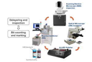
Figure 1: Illustration of typical PFA workflow for memory failure devices.
A typical PFA workflow for memory failure devices is illustrated in Figure 1. The workflow starts from RIE removing the inter-metal dielectric to expose the metal of each layer. Then it is followed by mechanical polishing using polisher with polishing slurry on the rotating cloth platen. During the polishing, optical microscope (OM) and scanning electron microscope (SEM) inspection are engaged to monitor and inspect the sample surface. When the sample reaches certain layers, bit-counting in the memory blocks of the device will be attempted to locate and mark the failed bits for TEM analysis.
In static random access memory (SRAM) devices, bit-counting in the memory blocks can be done as the sample reaches Metal2 (M2) or lower metal layer in which both bit lines (BLs) and word lines (WLs) are identifiable and countable. However, in the cases that request for critical dimension (CD) measurements on Via2 (V2) layer or cases where V2 deformation/void defect is highly suspected, traditional method of mechanically delayering away M3 that will damage part of V2 is no longer suitable. In non-volatile memory (NVM) devices, the memory bit-counting is even more challenging, since the metal layer (here it is M5) blocking the WLs directly lands on the memory cells (Figure 2a, b). There have been numerous FA studies on SRAM/NVM devices, from hard short/open failure [2-4] to subtle defect induced marginal failure [5-7]. After the electrical fault isolation (EFI) or bit-map analysis, memory bit-counting is the key step for TEM analysis or transistor-level probing to locate the defect. Prior to the laser deprocessing technique (LDT) assisted method was developed, there were two conventional methods of bit-counting used in SRAM/NVM device.

Figure 2: Typical circuit diagram (a) and bit-counting (b) of memory arrays in NVM devices.
One method is using focused ion beam (FIB) to remove M5 near the target BL to count the exposed cells as counting WLs. The other method is over-RIE the sample surface to expose and count the Memory Via (Mvia) as WLs (Figure 3). The first method has the advantages of real-time monitoring and localized milling, however it requires a FIB-SEM dual-beam system of which the cost is much higher than that of a SEM single-beam system, and much longer FA cycle time when the target memory bit is long distance from the memory block edge. The second method needs only a SEM single-beam system, but it comes with possible sample damage from the Pt protective pad missing the target memory bit. Besides this, for advanced technology node such as 28nm or below, the Mvia size deceases smaller than that of M5, which makes the method by over-RIE not workable. Therefore, new methods with fast cycle time and low cost for the bit-counting in memory devices are highly desired.
In this paper, we will introduce an innovative LDT assisted memory bit-counting method that is applicable to both SRAM and NVM devices. LDT is fast, simple, and has been used to secure an uneven sample surface and remove unwanted layers [1, 8]. LDT employs pulse laser with high peak power to irradiate the sample and physically remove material from the surface, which is economical, efficient, and user-friendly. Moreover, through a systematical parametric study, LDT is able to create uniform deprocessed surface in a large area on various types of materials.
2. Experiments
The experiments were conducted on a 40 nm SRAM device and a 28 nm NVM device. A mechanical polisher (ALLIED HighTech TwinPrep 5) with polishing cloth (Spec-Cloth), and polishing slurry (0.05 μm or 3 μm diamond suspension) was used for mechanical polishing. A SEM single-beam system (FEI MagellanTM 400L) equipped with a gas injection system was used for sample inspection and Pt marking. An optical microscope (ZEISS Axiotron) was used for optical inspection on the sample surface. For LDT, a laser system (New Wave Research Ezlaze3) was used for the sample deprocessing. The laser source emits a pulse laser (wavelength: 532 nm, energy range: 0 to 0.6 mJ, pulse width: ~5 ns) which was integrated into a probe station (Cascade Microtech PM5).
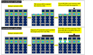
Figure 3: Conventional bit-counting methods for NVM devices.

Figure 4: Schematic illustration of LDT in NVM devices.
Parameters including laser output power, number of laser shots, and magnification of optical lens were studied on the dummy area of the NVM sample at M5 level. For different devices and materials, the same workflow can be followed to obtain the optimal parametric condition for laser deprocessing in each case. The window size of the laser is adjustable without power shift. Maximum size for 20× lens magnification was 150 μm × 150 μm. TEM sample preparation was performed using a FIB-SEM dual-beam system (FEI Helios NanoLab 450S). TEM analysis and energy dispersive X-ray (EDX) mapping were performed using a 200 kV Field Emission TEM (JEOL JEM-2100F) equipped with a SDD-EDX detector (Oxford X-MaxN 100TLE).

Figure 5: LDT assisted PFA workflow for memory failure devices.
2.1. Methodology
A schematic illustration of LDT in NVM devices is shown in Figure 4. Before the laser deprocessing on the target location, a series of parametric experiments were carried out on the dummy area. Figure 5 shows the LDT assisted PFA workflow for memory failure devices. Here the parametric variables include the work mode of laser energy, attenuation level, lens magnification, and the number of laser shots. For the selection of each parameter, we used parametric arrays to determine the optimal condition in terms of the surface uniformity of the deprocessed sample. A uniform sample surface is critical to the bit-counting accuracy. Any false counting could result in missing the defect.
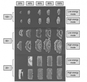
Figure 6: SEM images of the laser deprocessed surfaces of the NVM devices under different energy mode, attenuation level (%), and lens magnification.
2.2. Selection of laser power and lens magnification
Figure 6 shows the SEM images of the laser deprocessed surfaces of the NVM devices under different laser power and lens magnification. From the results, we can see that 100× and 50× lens created a very uneven and deformed surface with multiple layers exposed, regardless of energy mode and attenuation level. So we narrowed down the selection to 20× lens arrays. In low energy mode, 80% attenuation level delivered the most uniform deprocessed surface at the NVM cell level. In high energy mode, the best results were delivered by 40% attenuation level.
The surface uniformity of low energy mode at 80% attenuation level and high energy mode at 40% attenuation mode are comparable for the bit-counting, as shown in Figure 7. However, in low energy mode, the 100% attenuation level makes use of 0.2 mJ of energy while in high energy mode, at 100% attenuation level, the machine makes use of 0.6 mJ of energy. Therefore, output energy of 80% attenuation level in low energy mode is 0.8 × 0.2 mJ = 0.16 mJ, which is lower than 0.4 × 0.6 mJ = 0.24 mJ for 40% attenuation level in high energy mode. Considering the fact that lower laser energy is safer for the sample, low energy mode and 80% attenuation level were selected for the laser deprocessing for memory bit-counting.

Figure 7: High magnification SEM images of the laser deprocessed surfaces of the NVM devices under 40% attenuation level in high energy mode and 80% attenuation level in low energy mode.

Figure 8: SEM images of the laser deprocessed surfaces of the NVM devices under different number of laser shots.
2.3. Selection of number of laser shots
The experiments above were all from a single laser shot. In this section, using the lens and the attenuation level selected for each energy mode, a boundary test was performed on the maximum number of laser shots on the same surface before the surface becomes uneven again. In some cases, the layer on top of the bit-counting layer might be too thick and need more than one shot of laser to remove. Figure 8 shows the SEM images of the laser deprocessed surfaces of the NVM sample under different numbers of shots. It can be seen that the surfaces for each shot started to become uneven after the second shot was made on the same surface. This could be due to that the third shot was shone on the critical interface between the non low-k dielectric layer (memory cells and Mvia) and the ultra low-k dielectric layer (M4 and below). The unevenness was greatly increased during the third shot because of the big difference in the mechanical removal rate (up to 10 times) between the non low-k and the ultra low-k materials [9]. The experimental results would differ from case to case. For this NVM device, one shot of laser which created uniform bit-counting area (Figure 7) was selected.
2.4. Boundary limitations of laser shots
To understand the damage induced by laser shots to the memory bits, TEM analysis was done on the boundary of the laser deprocessed area. The results (Figure 9) show that four bits (Bit 1, 2, 3, 4) adjacent to the deprocessing area were damaged by the laser shot due to the thermal effect. Similar to other parameters, boundary limitations are dependent on the sample materials and surface conditions, and should be studied on the dummy area first to avoid damaging to the target bits.

Figure 9: SEM images of the laser deprocessed surfaces of the NVM devices under different energy mode, attenuation level (%), and lens magnification.
2.5. Operation procedure of LDT assisted memory bit-counting
The procedure steps below describe how to utilize LDT to perform the memory bit-counting in SRAM/NVM devices.
- Delayer the sample and stop at one layer before the bit-counting layer (M5 for NVM, M3 for SRAM) by mechanical polishing and inspection.
- Make a SEM Pt mark at the target BL as a “sight” for the laser deprocessing process in OM (this step can be skipped for SRAM devices with small memory blocks).
- Remove M5 (NVM) or M3 (SRAM) layer at certain distance (referring to the boundary limitations of laser shots) from the target BL to expose the memory cells by laser deprocessing (Figure 4). For SRAM devices, an extra deprocessed area for counting WLs is needed.
- Water-polish the sample to clean the laser burst debris off the deprocessed area.
- In the deprocessed area, count the exposed memory cells as WLs and M5 lines as BLs to locate the target bit from the NVM memory block (Figure 4). For SRAM devices, both WLs and BLs will also be identifiable and countable from M2 or below.
- Make SEM Pt marks on the located target bit accordingly for TEM analysis (Figure 4).
Table 1: Operation time usage (in hours) of the conventional methods and the new LDT method for NVM devices.
| Pt mark target BL | Deposit Pt protection layer | Over RIE | FIB milling | Laser deprocessing | Counts WLs | Total | |
| Conventional method 1 | N/A | ~0.6 | ~0.2 | N/A | N/A | ~0.7 | ~1.5 |
| Conventional method 2 | ~0.3 | N/A | N/A | ~0.8 | N/A | ~0.5 | ~1.5 |
| New method | ~0.3 | N/A | N/A | N/A | ~0.1 | ~0.5 | ~0.9 |
In Table 1, the operation time usage of the conventional methods and the new LDT method for NVM devices are compared, which is evaluated under the same experimental conditions. The time usage of each operation step may vary with different devices, requirements of the cases and experiences of the operators. It can been seen that the LDT method can shorten the time usage by up to 45%.
Table 2: Summary of the advantages and disadvantages of the conventional methods and the new LDT method.
| Advantages | Disadvantages | |
| Conventional method 1 | Localized milling, real-time monitoring | High cost, Long FA cycle time |
| Conventional method 2 | Low cost | Long FA cycle time, High risk of sample damaging, Not suitable for advanced technology node |
| New method | Low cost, Short FA cycle time | Sample dependent setting of laser parameters |
Table 2 shows the advantages and disadvantages of the conventional methods and the new LDT method. Although the new method needs parametric study on the sample, the one-time effort eventually significantly saves FA time and FA cost.
3. Results and Discussion
3.1. Case study on NVM device
In this case, a 28 nm NVM device was performed with PFA using LDT. Figure 10 is the M5 graphic data system (GDS) layout of the device. After wafer sort, the bitmap information was provided in the data log. According to the e-test results, the NVM chip suffered from single-bit short failure (Figure 10).
The sample was polished to M5 layer, and then continued with LDT for bit-counting (Figure 11). First, a 45° angled e-beam Pt line mark was deposited in SEM as the reference for the laser deprocessing below the target BL (located by M5 GDS layout), and was deposited long and thick (SEM: 10 kV at 0.8 nA; Rate of deposition: 10 μm [length] × 2 μm [thickness] in 5 mins) to be clearly visible in OM. Second, at around 20 BLs to the right of the target bit, LDT was used to create a laser exposed area at the level of memory cells, in which the WLs were counted and marked according to the WL address. Finally, Pt marks were deposited on the located target bit for the following TEM analysis.
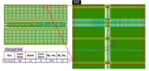
Figure 10: M5 GDS layout of 28 nm NVM device.
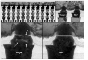
Figure 12: TEM images (Y direction along M5 as shown in Figure 11) of the failed bit and the reference bit.
TEM results of the sample are shown in Figure 12. From the TEM images, metal void and collapsed insulator layer were found at the failed bit. The metal void in the lower cell electrode should form in the first place, and then induce the uneven deposition of the insulation layer and the breakdown of the memory cell.
Figure 13 shows the scanning transmission electron microscope (STEM) images of another case where the TEM sample was cut across M5 to compare between different BLs from
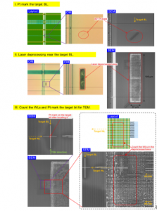
Figure 11: Schematic illustration of LDT assisted bit-counting at M5 in NVM devices.
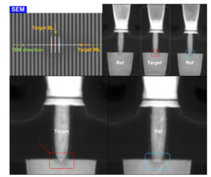
Figure 13: STEM images (X direction across M5) of the failed bit and the reference bit.
the same WL. From the results, abnormal profile at the bottom of the Mvia was found at the failed bit, which caused high landing resistance of the bit. It is worth to mention that, cutting along Y direction, even when the conventional methods aim at wrong WL by a few bits, the real target bit is usually still covered in the TEM sample so it can be corrected in the TEM analysis. However, in the X direction cut, wrong counting due to the insufficient exposing of the memory bits using conventional methods will result in missing the defect. Therefore, the LDT method offers the advantage of efficiently creating a bit-counting area and locating the target WLs in a high success rate.
3.2. Case study on SRAM device
In the SRAM case, a 40nm device with SRAM blocks was found to suffer from a 3-bits cluster failure. Through a series of analysis, Cu void defect in V1/V2 is suspected to result in the random wafer pattern, so the delayering must stop at M3 level to measure the V2 CD. However, without a reference, bit-counting at M3 is not practical, as seen from the GDS layout of SRAM devices (Figure 14). At M3, BLs and WLs are all not able to be properly identified. If we all the way polish to V2, the top portion of V2 will be damaged and the CD measurements will become impossible.
Figure 14: Typical GDS layout of SRAM devices.

Figure 15: TEM/STEM images of a failed SRAM sample preparation. Top portion of V2 has been damaged.

Figure 16: High/low magnification TEM imaging on the failed bits.

Figure 17: EDX mapping analysis on the failed bit. Defect of Cu void is observed, as arrowed in the Cu quant map.
Figure 15 shows a failed SRAM sample preparation. To solve the problem, we used LDT to create two reference areas (one for counting BLs and the other one for counting WLs) near the failed bit (Figure 18). In the reference areas, bits at V1/M1 level are clearly visible for the counting of WLs and BLs, while the target area is still at M3.
By counting and marking the WLs/BLs in the reference area, the failed bit was located and marked. TEM sample preparation was then performed on the marked bit. The TEM results are shown in Figure 16. From the high/low magnification TEM images, metal void was found at the bottom of V1. CD measurement on V2 was also taken. EDX analysis was then performed on the void area (Figure 17), in order to study the mechanism of the void formation. The EDX quant maps showed that Cu diffusion/migration occurred at the arrowed void area. Therefore, oxidation/corrosion
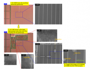
Figure 18: Schematic illustration of LDT assisted bit-counting at M3 in SRAM devices.
of the seed Cu layers could be the root cause of the failure. The high aspect ratio of the metal trench in the dual damascene process could introduce thinner seed Cu layer at the trench bottom. In the subsequent bulk Cu plating, the H+ ions in the electrolyte may attack the Cu seed layer as an acid etchant, since the electrons in the current flowing through the thinning portion were not enough to neutralize the excess H+ ions. This would finally induce the formation of the void at the bottom of either V1 or V2.
4. Conclusion
In this paper, an innovative LDT assisted PFA technique is fully exploited and discussed. Compared to the conventional methods that involve high-cost equipment, this new method employing a pulse laser system instead significantly lowers the FA cost (by more than 5 times) and shortens the FA cycle time (by up to 45%), and facilitates potential applications in other FA areas such as pre-EFI sample preparation, large size cross-sectional analysis, etc. Moreover, only basic FA skills such as using OM and SEM are required to manipulate this new method which is suitable for FA engineers from all different levels.
Conflict of Interest
The authors declare no conflict of interest.
Abbreviations
BL Bit-Line
CD Critical Dimension
EDX Energy Dispersive X-ray
EFI Electrical Fault Isolation
FA Failure Analysis
FIB Focused Ion Beam
GDS Graphic Data System
IC Integrated Circuit
LDT Laser Deprocessing Technique
Mvia Memory Via
Mx Metalx, x is layer number
NVM Non-Volatile Memory
OM Optical Microscope
PFA Physical Failure Analysis
RIE Reactive Ion Etching
SEM Scanning Electron Microscope
SRAM Static Random Access Memory
STEM Scanning Transmission Electron Microscope
TEM Transmission Electron Microscope
Vx Viax, x is layer number
- H. H. Yap, P. K. Tan, L. Zhu, H. Feng, Y. Z. Zhao, R. He, H. Tan, B. H. Liu, Y. M. Huang, D. D. Wang, J. Lam, Z. H. Mai, “Application of Laser Deprocessing Technique in PFA on Chemical Over-etched on Bond-pad Issue,” Microelectronics Reliability, 64, 357-361, 2016, doi:10.1016/j.microrel.2016.07.057.
- S. Ikeda, Y. Yoshida, K. Ishibashi, Y. mitsui, “Failure Analysis of 6T SRAM on Low-voltage and High-frequency Operation,” in 2003 IEEE Transactions on Electron Devices, 1270-1276, 2019, doi:10.1109/TED.2003.813474.
- Z. G. Song, “SRAM Failure Analysis Evolution Driven by Technology Scaling,” in 2014 IEEE International Symposium on Physical and Failure Analysis of Integrated Circuits (IPFA), 2014, doi:10.1109/IPFA.2014.6898207.
- P. Egger, C. Burmer, “SRAM Failure Analysis Strategy,” in 2003 International Symposium for Testing and Failure Analysis (ISTFA), 177-183, 2003.
- C. Q. Chen, P. T. Ng, S. P. Neo, P. K. Tan, A. C. T. Quah, J. Zhu, “Application of Nanoprobing on Subtle Defects in the Embedded Non-volatile Memory Device,” in 2019 International Symposium for Testing and Failure Analysis (ISTFA), 2019.
- W. T. Chang, T. E. Hsieh, “Advance Static Random Access Memory Soft Fail Analysis Using Nanoprobing and Junction Delineation Transmission Electron Microscopy,” Journal of Vacuum Science & Technology B: Microelectronics and Nanometer Structures Processing, Measurement, and Phenomena, 25, 202, 2007.
- T. Mizutani, T. Saraya, K. Takeuchi, M. Kobayashi, T. Hiramoto, “Transistor-level Characterization of Static Random Access Memory Bit Failures Induced by Random Telegraph Noise,” Japanese Journal of Applied Physics, 55, 04ED05, 2016, doi:10.7567/JJAP.55.04ED05.
- Y. Z. Zhao, Q. J. Wang, P. K. Tan, H. H. Yap, B. H. Liu, H. Feng, H. Tan, R. He, Y. M. Huang, D. D. Wang, L. Zhu, C. Q. Chen, F. Rivai, J. Lam, Z. H. Mai, “Application of Fast Laser Deprocessing Techniques on Large Cross-section View Area Sample with FIB-SEM dual beam system,” Microelectronics Reliability, 64, 362-366, 2016.
- Y. L. Pan, P. K. Tan, S. L. Ting, C. Q. Chen, “Advanced Sample Preparation Techniques for Rescuing Damaged Samples with Cracks, Scratches, or Unevenness in Delayering,” in 2020 IEEE International Symposium on Physical and Failure Analysis of Integrated Circuits (IPFA), 2020.