
Essential Features/Issues of a Multi-Phase Switching Synchronous Buck Regulator
Volume 5, Issue 5, Page No 1056-1063, 2020
Author’s Name: Hani Ahmad-Assia), Nour Sultan Gammoh, Mariana Awni Al Bader
View Affiliations
Electrical Engineering Department, King Abdullah II School of Engineering, Princess Sumaya University for Technology, Amman, 11941, Jordan
a)Author to whom correspondence should be addressed. E-mail: h.ahmad@psut.edu.jo
Adv. Sci. Technol. Eng. Syst. J. 5(5), 1056-1059 (2020); ![]() DOI: 10.25046/aj0505130
DOI: 10.25046/aj0505130
Keywords: Multi-phase buck converter, Phase shedding, Fast-transient, Current sensing

Export Citations
This paper addresses essential features/issues and proposes solutions that would improve the overall performance of a multi-phase buck converter. Low efficiency at light load is addressed with phase shedding, load fast transient and regulated output voltage spiking/dipping is addressed with novel helper technique at the point of load (output node). An Integrated current sensing is utilized to implement over-current-protection (OCP), in addition to its inherent function in current mode control. The phase shedding developed technique was used to enhance the efficiency of the converter. The number of phases rather increases or decreases, depending on the desired load. The proposed fast transient helper circuit is tested by inserting a 500mA transient current step in 100µs. Worst case spike of a 79.1mV was achieved at the output node; which is a reduction of 49.4% of the original response (160mV without the helper circuit). Worst case of a 35mV of output voltage dip was achieved; which is a reduced by 45.4% compared to the original response (77.1mV without the helper circuit). An integrated current sensing technique using current mirroring to equalize the drain voltages of main and replica (sense) PMOS devices was utilized. With this technique, the current in the replica (sense) PMOS device is a scaled down version of the current in the main PMOS device. The sensed currents from all three phases are added up and converted to a voltage. This voltage is compared to a reference voltage that represents the limit for over-current. This reference voltage is set to be 20% higher than the average total currents in the three phases combined.
Received: 30 August 2020, Accepted: 28 September 2020, Published Online: 20 October 2020
1. Background
This paper is an extension of work originally presented in Power Electronics and Drive Systems (2019 IEEE 13th International Conference on PEDS). Unlike single phase converters, multiphase buck converters are considered one of the state-of-art regulator topologies that provide high current capability (example, some CPUs requires 10A-15A or even more at their peak performances). Compared to a single-phase converter, multi-phase converters were proven to have many benefits, such as higher efficiency, lower component sizes, and reduced output current and voltage ripple [1].
Different features and techniques are addressed in this paper to study the behaviour of the multiphase buck converter. In [2], phase shedding (PS) is defined as a technique used to improve the converter efficiency by disconnecting some phases at light load. When the load decreases, there is no need for using all the phases in the circuit, however, it is possible to reduce the number of phases as the output current is being distributed between those reduced phases. In [3], fast transient is presented as a technique that will guarantee a low transient spike/dip and preserve a stable supply voltage. The two main objectives for using the fast transient are having the shortest recovery time and having the smallest output voltage spike/dip. In [4], integrated current sensing was presented as a technique to implement over-current protection (OCP), and current-mode feedback control. Many different schemes have been executed to utilize the inductor current sensing techniques. Most of these current sensing schemes have limiting constraints such as high-power dissipation, difficult implementation and control, and process-dependence..
2. Features/Issues
In [1], the single-phase buck converter was used as a first step to develop a functional multi-phase buck converter. In this paper, it was also used to test the features added to the final multi-phase design (consists of power and control stages). The buck converter (the power stage) was designed by sweeping the width of both NMOS and PMOS transistors so that it would handle the current passing through them. The width of the NMOS was chosen to be 23m and the width of the PMOS which is usually 2-3 times larger than the width of the NMOS, was chosen to be 53.2m. These sizes were selected based on RdSon which is designed to be within the typical industrial standard range of (50-100) mΩ.
This paper discusses three features/issues that will be added to the power stage of the design, starting from single phase to the three-phase final design. This is done to observe the impact of the features on each phase. The three features/issues are Phase Shedding, Fast Transient, and Integrated current sensing which will be discussed in the sub-sections A, B, and C.
The schematic design and simulation results of the proposed circuits were done in LTspice using 180nm standard CMOS technology [5].
2.1. Phase Shedding
Phase Shedding technique is defined as the disconnection of phases in multi-phase buck converters when using different loads. This technique is a requirement to achieve the highest efficiency possible. To implement this feature, an NMOS transistor is utilized to realize an ON/OFF switch function as shown in
Figure 1. This NMOS is added to the single-phase buck converter and placed at the output node as shown in Figure 2. An NMOS was chosen due to its smaller size and faster response when it is compared to a PMOS device. To make an NMOS transistor turns on, a voltage source (Vsource) is connected to its gate and to make it turns off, its gate is grounded.
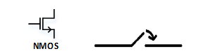
Figure 1: NMOS is used to implement an ON/OFF switch
Vsawtooth in the control stage is adjusted depending on the number of phases in the circuit. In multiphase converter, phase difference is applied to specify the angle that will be used depending on the number of phases in the circuit. Equation 1 was used to define the angle for each implementation. For single phase, the angle is at 0°. For two-phases, the angles are at 0° and 180°. For three-phases, the angles are at 0°, 120°, and 240°. As the number of phases increases, the ripple at the output is reduced.
Single-phase buck converter is utilized to test this phase shedding technique as shown in Figure 2. In this case, Vsawtooth was considered to be at 0°. The parameters used in the single-phase design are listed in Table 1: Parameters for the single-phase buck converterTable 1 with Vin = 3.3V, Vref = 1.2V, and Vsupply = 2.19V.
Table 1: Parameters for the single-phase buck converter
| Power stage | Control stage |
| Inductor (L1) = 2.17µH | Resistor (R2) = 13.3kΩ |
| Capacitor (C1) = 15µF | Resistor (R3) = 12.2kΩ |
| Resistor (R1) = 2.5Ω | Resistor (R4) = 53.7kΩ |
| Capacitor (C2) = 86.07µF | |
| Resistor (R5) = 100kΩ | |
| Capacitor (C3) = 0.318nF |
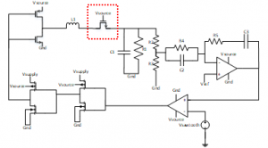
Figure 2: Single-phase Buck converter with NMOS switch used for Phase Shedding
When the NMOS is ON, the output voltage is 2.5V and the output current is 1A as seen in Figure 3.

Figure 3: Output voltage and load current when switch is ON
Since the single-phase converter has the minimum number of phases, there is no need to turn off the NMOS switch. Therefore, a two-phase converter was used next to implement the effect of phase shedding as seen in Figure 4. The resistor R1 is a simple representation of the load impedance. Based on Ohm’s law, and since the voltage is fixed (regulated), the current is changing (due to adding a phase). Since the current is changing, R1 is changed to fit the number of active phases (each phase adds same amount of current in this scenario). For two phase case, R1 is 1.25Ω and Vsawtooth was considered to be the summation of two signals at 0° and 180°.
Figure 4: Two-phase Buck converter with NMOS switches used for Phase Shedding
When both N1 and N2 are ON, this means that both phases are being active. In this case, the output voltage is 2.5V and the output current is 2A, having 1A distributed in each phase as demonstrated in Figure 5. When N1 is ON and N2 is OFF, or vice versa, R1 is changed to 2.5Ω due to the number of active phases being decreased. This is donebased on equation 1 above and it consequently maintains output voltage at 2.5V. The output current is now 1A as observed in Figure 6. The results are summarized in Table 2.
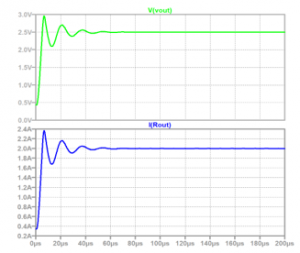
Figure 5: Output voltage and load current when both switches are ON
Table 2: Phase shedding results for two switches
| N1 | N2 | Voltage / V | Current / A |
| ON | ON | 2.5 | 2 |
| ON | OFF | 2.5 | 1 |

Figure 6: Output voltage and load current when one of the switches is ON
Applying this technique to the three-phase buck converter means having different load and different Vsawtooth. In three-phase scenario, R1 is decreased to 0.833333Ω and the summation of three sawtooth signals is used at 0°, 120°, and 240°. Figure 7 depicts this implementation.
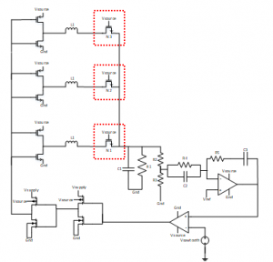
Figure 7: Three-phase converter with NMOS switches used for Phase Shedding
When N1, N2, and N3 are all ON, all phases are used, resulting in having an output voltage of 2.5V and an output current of 3A, having 1A distributed in each phase as shown in Figure 8. When N1 and N2 are ON and N3 is OFF (one phase is OFF), the used R1 is 1.25Ω as it is similar to the two-phase buck converter. The output voltage remains 2.5V and the output current is 2A (1A in each phase) as observed in Figure 9. When N1 is ON and N2 and N3 are OFF (one phase is ON), the simulation results are similar to the single-phase buck converter having 2.5V as an output voltage and 1A as an output current as depicted in Figure 10. The results are summarized in Table 3.
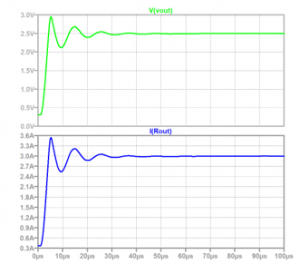
Figure 8: Output voltage and load current when all switches are ON
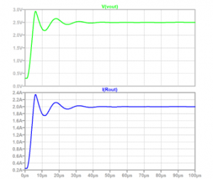
Figure 9: Output voltage and load current when one of the switches is OFF
Table 3. Phase shedding results for three switches
| N1 | N2 | N3 | Voltage / V | Current / A |
| ON | ON | ON | 2.5 | 3 |
| ON | ON | OFF | 2.5 | 2 |
| ON | OFF | OFF | 2.5 | 1 |
2.2. Fast-Transient
As previously discussed, a current source can be used to force a step in the load current which would cause a spike or a dip in the output voltage [1]. The importance of the fast-transient feature is that the current profile of modern high-performance devices (such as a microprocessor) is very dynamic in nature which means a change from few microamps to full peak value within very small interval of time (say microseconds or even less) is expected. This definitely causes a spike/dip in the regulated output voltage. The dip below 10% of the regulated voltage may cause malfunctioning of the devices in the circuit. A spike above 10% of the regulated output voltage may cause damage to some devices (exceeds breakdown voltage).

Figure 10: Output voltage and load current when one of the switches is ON
A transient current was inserted to test the response time that would take the controller to pull back the output to its regulated state and to measure the amount of worst spike/dip of the output voltage. In this paper, the current source with pulse signal of 500mA step (in both directions) was added parallel to the load to force the output voltage spike or dip. To mitigate/prevent this kind of problem, a proposed two-part circuitry was developed to assist in minimizing the voltage spike and dip to stay within the tolerable range. The developed solution is shown in Figure 11. The main job of the resistor voltage divider in helper circuit is to put the initial value for the gate voltage such that the transistor is off in the normal operating conditions (no load transient).
When spike occurs at the Vout node, the capacitor (C1) acts as a short circuit (due to high frequency signal of the fast-current step) which causes the gate voltage to increase. Therefore, NMOS transistor immediately starts to turn on. To overcome the spike, NMOS transistor starts pulling current from Vout node and this brings the spike back toward the regulated value. Results are shown in Figure 12 to Figure 15.
Table 4: Parameters of the helper circuits
| Spike | Dip |
| Resistor (R1) = 30kΩ | Resistor (R3) = 32kΩ |
| Resistor (R2) = 1kΩ | Resistor (R4) = 1kΩ |
| Capacitor (C1) = 10µF | Capacitor (C2) = 1µF |
| NMOS size= 70mm | PMOS size= 200mm |
When dip occurs at the Vout node, the capacitor (C2) acts as a short circuit which causes the gate voltage to decrease. Hence, PMOS transistor immediately starts to turn on. To overcome the dip, PMOS transistor starts pushing current to Vout node and this
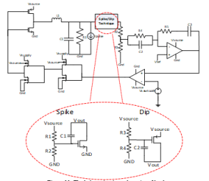
Figure 11: The helper circuits at the point of load
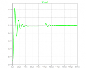
Figure 12: Output voltage spike without the helper circuit

Figure 13: Zoomed-in graph when spike occurs without helper circuit
brings the output voltage back towards its regulated value. Results are shown in Figure 16 to Figure 19. The values of the helper circuits are shown in Table 4.
This fast-transient technique is introduced to the three-phase buck converter. One of the benefits is that the voltage ripple decreases as the number of phases in the circuit increases [1].
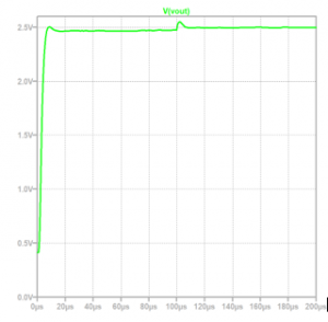
Figure 14: Output voltage spike with the helper circuit

Figure 15: Zoomed-in graph when spike occurs with helper circuit
Table 5: Fast Transient results
| Fast transient | Before the helper circuit | After the helper circuit |
| Spike | 160mV | 79.1mV |
| Dip | 77.1mV | 35mV |
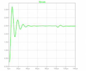
Figure 16: Output Voltage Dip without the helper circuit

Figure 17: Zoomed-in graph when dip occurs without helper circuit
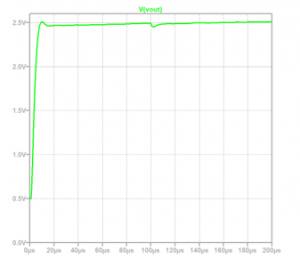
Figure 18: Output voltage Dip with the helper circuit

Figure 19: Zoomed-in graph when dip occurs with helper circuit
2.3. Integrated Current Sensing using Current Mirroring
Current sensing can be achieved using many conventional techniques such as Series-Sense Resistor [6]. This a simple technique that uses a resistor in series with an inductor is depicted in Figure 20. When knowing the value of the resistor, the voltage sensed across it will determine the current flowing through the inductor. This method allows higher power loss therefore, it has negative impact on the efficiency of the converter. The series resistor method can also be used by placing the sense resistor in series with the PMOS or NMOS.
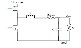
Figure 20: An example of series resistor used in current sensing
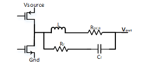
Figure 21: Integrated current sensing by adding a parallel capacitor Cf to the convertor’s inductor L
DC resistance (DCR) of switching inductors with a low-pass RC circuit connected in parallel with the inductor is considered to be another method to sense the current as presented in Figure 21 [4]. The disadvantage of using this method is that the RC circuit has to be chosen based on the inductor and resistor values which is not an easy task as some components are integrated, and others are not.
An Op-Amp can also be used as an additional method for a current sensing technique as shown in Figure 22 [6]. The Op-Amp is used to force the drain voltages of the transistors (power and sense) in the DC-DC converters to be equal. However, if the power and sense transistors width ratio increase (for efficiency reasons), the accuracy of the circuit degrades. The Op-Amp needs to have a high bandwidth and a high gain to have a very accurate current sensing method. Practically, there is not an Op-Amp that complies perfectly to the previous requirements.

Figure 22: Integrated current sensing using op-amp and sense FET
The selected method for current sensing is the current mirroring circuit [7]. This method is selected due to the higher accuracy in addition to higher efficiency it provides compared to the previous mentioned methods. As shown in Figure 23, MP2 was connected to be a replica (sense) device for MP1. The two sources and gates are physically connected. The drains of these two devices are forced to be equal via the current mirror. Of course, each terminal of the main device and the corresponding sense device need to be equal in value since the both main and sense devices act as switches. The relationship between MP1 and MP2 sizes is presented as a ratio of 1: K. The drain currents flowing through MP1 and MP2 then will have a value of Ip1 and Ip2 which equals to Ip1/K.
In this current-sensing circuit, to have accurate current sensing, the voltages at NB and NC need to be almost equal (drain voltages for main and sense devices). As MP1 and MP2 are turned on, then MN1 is turned off, therefore the voltage at NB and NC is high because of currents Ip2 and Isense are equal and vice versa. This method can force the voltages at nodes NB and NC to be equal as noticed in Figure 24. The width of the transistor MP1 was chosen to have a value of W1 and transistor MP2 was chosen to have a width of W2 which equals to W1/K.
For the current mirror transistors, size sweeping/optimization was conducted to equalize both nodes NB and NC.
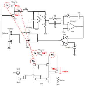
Figure 23: Integrated current sensing based on current mirror

Figure 24: Voltages at Nodes NB and NC
Figure 25 shows the currents Ip1 and Ip2. It can be observed that Ip1 is identical to Ip2 except for the scaling factor of 1: K (Ip2=Ip1/K).
The sensed voltage across Rsense represents the output current of the converter. The output current can be sensed using two different options. The first option is by assuming that all phases are balanced and carry the same current which is 1A per phase. In this case, a single-phase converter can be used to represent whether an over-current condition has occurred or not. Therefore, a single-phase is enough to represent the total current of multi-phase converter. If Isense for the single phase is exceeded by 20% of a reference value, an over-current has occurred and switching will be halted.

Figure 25: Ip1 and Ip2 of main and sense PMOSs

Figure 26: Option two combined sensed current for Three-Phase

Figure 27: Three-Phase OCP indicator
Another option is possible by combining sensed currents of all phases together regardless of having the current being balanced between phases or not. In this case, the combined current, which is the total current of the converter, is 3A. A reference voltage with a value of 1.2V is presented to assist in detecting an over-current. The sensed voltage is compared to the reference voltage, therefore, if the sensed voltage value is higher than the reference voltage, then no over-current has occurred and vice versa. Of course, this 1.2V is a reference voltage that represent 20% higher than typical 3A. When over-current has occurred then the switching must be halted to protect the circuit. The second option was selected in this paper due to its higher practical value with the assumption of no current balancing. As a result, no over-current was detected in the final design as seen in Figure 26 and Figure 27.
3. Conclusion
It is well known that a multi-phase buck converter has higher capabilities, and efficiency compared to the single-phase buck converter. The phase shedding technique was implemented in the three-phase buck converter utilizing NMOS switches as they are used to disconnect some phases at light load. When the load decreases, there is no need for using all the phases in the circuit. It was concluded that by increasing the number of phases, the efficiency would be improved.
The proposed fast transient helper circuit is tested by inserting a 500mA transient current step in 100µs. Worst case spike of 79.1mV was achieved; which is a reduction of 49.4% of the original response (160mV) without the helper circuit. Worst case of 35mV of a voltage dip was achieved; which is a reduced by 45.4% compared to the original response (77.1mV) without the helper circuit. Moreover, the integrated current-sensing technique using current mirroring was used in the three-phase buck converter to detect the occurrence of an over-current, in order to protect the components in the circuit. A reference voltage with 20% higher than typical value is used to indicate an occurrence of an over current.
- N. S. Gammoh, M. A. Al-Bader and H. Ahmed-Assi, “Design and Simulation of a Three-Phase Switching Synchronous Buck Regulator,” 2019.
- A. Costabeber, P. Mattavelli and S. Saggini, “Digital Time-Optimal Phase Shedding in Multiphase Buck Converters,” 2010.
- Y. Zeng and H.-z. Tan, “Fast-transient DC-DC converter using an amplitude-limited error amplifier with a rapid error-signal control,” 2019.
- Y.-S. Roh, Y.-J. Moon, J. Park, M.-G. Jeong and C. Yoo, “A Multiphase Synchronous Buck Converter With a Fully Integrated Current Balancing Scheme,” 2015.
- 6 January 2012. [Online]. Available: http://ptm.asu.edu/modelcard/180nm_bulk.txt.
- H. P. Forghani-zadeh and G. A. Rincon-Mora, “Current-Sensing Techniques for DC-DC Converters,” 2002.
- C.-H. Chang and R. C. Chang, “A Novel Current Sensing Circuit for a Current-Mode Control CMOS DC-DC Buck Converter,” 2005.