Low Power Bulk Driven Series Parallel OTA for Low Frequency Applications

Adv. Sci. Technol. Eng. Syst. J. 5(5), 69–73 (2020);
 DOI: 10.25046/aj050510
Low power OTAs are the most preferred circuits in the realization of continuous time filters of analog front end of wearable healthcare devices. A low transconductance OTA with series parallel current mirror to realize large time constant of the filter is designed. The differential pair of the OTA uses bulk driven PMOSFETs and the subthreshold operation of the circuit achieves 44 nW power with supply voltage of ±0.4 V. The designed OTA has DC gain of 29.59 dB and UGBW of 34.28 KHz. Using the proposed OTA, a multifunction filter which can operate as low pass and high pass filter, having cut-off frequency in the range 25 Hz – 225 Hz is designed in gpdk 180 nm CMOS technology. The simulation is performed using Cadence virtuoso design environment.
1. Introduction
Energy efficient wearable biomedical devices are most widely used in modern healthcare services. In such systems, the design of analog front end (AFE) circuits using existing CMOS technology has multiple design constraints having tradeoffs. As the AFE circuits need to remain on all the time to sense the bioelectric signals continuously, they consume largest share of the overall power budget. So, the energy efficiency of these circuits is major concern along with other performance parameters.
As shown in Figure 1, the analog front end (AFE) consists of low noise amplifier followed by continuous time active filters. Using the sensors or electrodes, biomedical signals such as ECG, EEG, EMG etc. are captured. These signals are having amplitude in the range of µV to few mV and frequencies in the range of dc to few Hz. Therefore, these circuits have to be designed with good low frequency performance. As the signal from the electrodes has dc component, large off chip capacitors are used. However, use of subhertz cutoff frequency high pass filter eliminates these large capacitors. The low pass and band pass filters are used to select the required signal.
The analog filters were designed using opamps. The bandwidth of opamp-RC filters is limited by the excessive gain-bandwidth product requirement for the opamp, to obtain ideal filter response. The high gain-bandwidth product of opamp based topologies consume more power. Therefore, in recent designs, Operational Transconductance Amplifier (OTA) are used in place of opamps. OTAs are also used as the low noise amplifier (LNA), where they need to have high gain and less noise. Therefore, OTA is an important circuit in the analog front end (AFE) of low power systems. OTA is a voltage controlled current source and it converts differential input voltage to output current. The circuit symbol for OTA is shown in Figure 2.
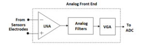
Figure 1: Block diagram of analog front end

Figure 2: Circuit symbol for OTA
Figure 3 shows the circuit diagram of single ended current mirror OTA with bulk driven PMOS differential pair, where all nodes have either drain-gate connected or source connected MOSFETs except for input devices. The diffential input ( Vin+ – Vin- ) is applied to the bulk terminal of PMOSFET pair M1 and M2 that results in output current given by (1). The transconductance of the OTA is constant for the specifies range of differential input and is controlled by bias current Ibias.
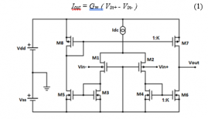
Figure 3: Schematic of current mirror OTA with bulk driven PMOS differential pair
The low voltage operation of OTA is necessary for low power operation. In strong inversion region operating voltage cannot be lowered below the threshold voltage of the MOSFETs. The state of the art digital circuits are operating at 0.3 V to 0.5 V range. To make analog circuits work with same supply voltage range in a chip, they are operated in subthreshold or weak inversion region by choosing appropriate inversion level [1][2]. To lower the operating current level bulk driven MOSFETs are used, resulting in low transconductane and increased linearity. The bulk driven MOSFETs have low cutoff frequency leading to poor frequency response characteristics. The low frequency operation requires large time constants which can be achieved by designing OTAs with small transconductance. In weak inversion gm/Id is high. In order to reduce gm series parallel current mirror [2] is used wherein small bias current and large division factor is used to reduce the output current. Choice of small bias current leads to poor input linear range. Compared to low transconductor design techniques like current division [3], bulk driven [4], attenuator based modular reduction of transconductance [5], current steering [6], source degeneration [7], current cancellation and series parallel current division technique gives lowest transconductance, low offset and better linearity. However, there is trade off with low power.
The proposed series parallel bulk driven OTA (SPOTA) is explained in section 2. The simulation results of the OTA is discussed in section 3. In Section 4, second order multifunction Gm-C filter with tunable cut-off frequency as an application of the proposed SPOTA is explained followed by conclusion in Section 5.
2. Proposed Bulk Driven Series Parallel OTA
In low power analog designs, choice of circuit topology significantly matters for power reduction. In the design of analog filters, OTAs are suitable alternative for opamps. The transconductance of the OTA is an important parameter in the design of active filters. In analog filter applications, the transconductance value is chosen depending on the cutoff frequency range. For low cut off frequency analog filters, large capacitors and resistors are required. As integration of the large resistor is not area efficient, small transconductance cells are designed. In series parallel current division technique, output current is divided by high ratio to achieve very small transconductance [2]. The bulk driven PMOSFET differential pair further reduces overall transconductance.
The OTA shown in Figure 3 is modified to obtain bulk driven series parallel (SP) OTA as shown in Figure 4. The differential input voltage is connected to the substrate of PMOSFETs M1 and M2 and the gates are connected to . Therefore, the transconductance of the OTA depends on , the body conductance which is 0.2 to 0.4 times , the transconductance of the MOSFET. The bulk driven PMOS differential pair at the input with series-parallel current mirror load reduces the transconductance and increases the linearity of the OTA. All devices in the circuit are biased to operate in weak inversion region, by maintaining gate voltage VGS < Vth , the threshold voltage and drain to source voltages . The weak inversion drain current under these condition is as given in (2),
ID = 2 n K VT2 ( W / L ) exp( ( VGS – Vth ) / n VT ) (2)
where K = µnCox, the process dependent parameter which is the product of mobility of charge carrier and the unit gate capacitance, is the volt equivalent of temperature approximately equal to 26 mV at room temperature and n is given by (3),
n = ( gm + gmb ) / gm (3)
The transconductance gm in subthreshold region is as given in (4),
gm = ID / n VT (4)
Also, the drain conductance go is expressed as in (5),
go ≈ λ ID (5)
The current mirror load of the differential pair has series and parallel placed MOSFETs so that output current is small. The overall transconductance of the OTA is calculated using (6),
Gm = gmb1 / N2 (6)
where gmb1 is the body transconductance of PMOS M1 and N is the number of series-parallel connected transistors of current mirror load of the differential pair. The current source Idc is realized using PMOS current mirror to provide bias current.
The voltage gain of the circuit is given by (7), with K=1.
Av = gmb1 / ( go7 + gon ) (7)
where gon is the overall output conductance of series connected NMOSFETs at the output node. The unity gain cutoff frequency is given by (8),
fT = gmb1 / 2 π CL (8)
The transconductance in pS to few nS can be realized when current is divided at the load instead of at the input side. The advantages of series parallel current mirror OTA are low input noise, wide linear input range, small transconductance and nano watt power. This OTA is used as Gm-cells of a second order Gm-C filter.
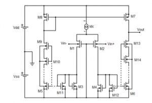
Figure 4: Schematic of proposed bulk driven series-parallel OTA
3. Discussion on Simulation Results of SPOTA
The series parallel current division technique is applied to the current mirror OTA for gate driven and bulk driven input PMOS differential pair. Using the spectre simulation in Cadence Virtuoso tool power dissipation, DC gain, unity gain bandwidth, transconductance, gain and phase margin of circuit are determined and compared. The CMOS technology used is gpdk 180nm. The gate driven SPOTA has power supply of 1.6 V while bulk driven circuit is operated at supply voltage of ± 0.4 V. The input and output waveforms of the bulk driven SPOTA is shown in Figure 5. For ± 1mV input, output voltage of 128 mVpp is obtained. The DC gain is 29.59 dB and 44 nW of power is consumed as can be seen in Figure 6 and in Figure 7 respectively. The SPOTA is stable with 53o of phase margin and has gain margin of 28.2 dB. The OTA has unity gain cutoff frequency of 34. 28 kHz and CMRR of 74.68 dB. The output is linear for ± 50 mV differential input voltage, which is a good range for biomedical applications.
Table 1 gives the comparison of bulk driven SPOTA with gate driven circuit. It is observed that the bulk driven MOSFETs can be operated with supply voltage near the threshold voltage, while for gate driven MOSFETs overdrive voltage requirement has to be met. Therefore, gate driven SPOTA with 1.6 V supply voltage has higher power consumption of 194.336 nW whereas bulk SPOTA power is reduced to 44 nW. The transconductance of the OTA is function of bias current. For bulk driven circuits,

Figure 5: Input and output waveforms of bulk driven SPOTA
Figure 6: Plot of DC gain and phase of bulk driven SPOTA

Figure 7: Power dissipation curve of SPOTA
the operating current can be very small. A transconductance of 6.03 nS for bulk driven and 24.63 nS for gate driven is achieved using series parallel technique for N=7 and can be reduced to pS by choosing large value for N. Hence the transconductance of the bulk driven SPOTA is small compared to that of gate driven at the cost of reduced bandwidth, gain margin and phase margin. The CMRR is improved in bulk SPOTA.
4. Gm-C Filter Design
The SPOTA proposed has small transconductance, hence its use in analog filter design for low frequency applications is demonstrated. The circuit structures in CMOS for active filters include Gm-C, OTA-C, switched capacitor integrator and Opamp-RC structures. The Gm-C filter is preferred because of its simplicity, ease of cascading, less area and minimum power consumption.
Table 1: Comparison of Bulk Driven SPOTA with Gate Driven SPOTA
| Design Parameter | Gate SPOTA | Bulk SPOTA |
| Technology (nm) | 180 nm | 180 nm |
| (V) | 1.6 | 0.4 |
| Bandwidth (kHz) | 74.93 | 3.504 |
| DC gain (dB) | 21.15 | 29.59 |
| Phase Margin | 62.6o | 53o |
| Gain Margin (dB) | 38.1 | 28.2 |
| CMRR (dB) | 62.96 | 74.68 |
| Transconductance | 24.63 nS | 6.03 nS |
| Power (nW) | 194.336 | 44 |
Gm-C filters rely on OTAs and capacitors to realise the transfer function of the filter. Since the transconductance of proposed SPOTA is less than 10 nS and can be even pS if N is chosen large, the integrated capacitor value can be limited in the order of fF to few pF. A second order Gm-C filter realized using biquad structure [8] [9] is shown in Figure 8. It can be set as low pass or high pass filter using the inputs Vin LP and Vin HP. The two OTAs are used in unity gain mode. For low pass filter, the input is connected to Vin LP with Vin HP grounded, whereas it is connected to with grounded for high pass filter. The filter is synthesized by neglecting the nonidealities. In Figure 8, voltage V1 is as given by (9),

Figure 8: Block schematic of biquad Gm-C filter
Also, the output voltage is as given by (10),
Vout = (Gm2V1 + sC2Vin HP ) / (sC2 + Gm2) (10)
Substituting (9) in (10) we obtain the output voltage Vout as in (11),
Vout (s) = ((Gm1 Gm2 / C1 C2 ) Vin LP + S2 Vin HP ) / ( s2 + s ( Gm2 / C2 ) + Gm1 Gm2 / C1 C2 ) (11)
Choosing Gm1 = Gm2 the transfer function of biquad Gm-C low pass filter is obtained by setting Vin HP = 0 and is given by (12),
HLP(s) = (Gm2 / C1 C2 ) / ( s2 + s ( Gm / C2 ) + Gm2 / C1 C2) (12)
Similarly, the transfer function of high pass filter is obtained by setting Vin LP = 0 and is given by (13),
HHP(s) = s2 / ( s2 + s ( Gm2 / C2 ) + Gm1 Gm2 / C1 C2 ) (13)
The 3 dB cutoff frequency and the quality factor of the filter is as given in (14),
fc = (1/ 2π ) sqrt ( Gm2 / C1 C2 ) and Q = sqrt ( C2 / C1 ) (14)
5. Simulation Results of Biquad Gm-C Filter
The simulation of biquad Gm-C filter is carried out using Cadence Virtuoso Tool with gpdk180nm CMOS technology. The magnitude response of the low pass and high pass filter are shown in Figure 9 and Figure 10. The proposed OTA connected as voltage follower is used as Gm cell. The filters have butterworth magnitude response with cutoff frequency in the range 25 Hz to 225 Hz for C1 = 10 pF. Gain and power consumption are around -7.4 dB to -7.8 dB and 91.7 nW respectively.

Figure 9: Magnitude response of low pass filter using bulk driven SPOTA
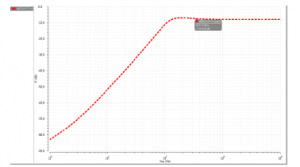
Figure10: Magnitude response of high pass filter using bulk driven SPOTA
By varying capacitor values or by varying the bias current to SPOTA, required cutoff frequency for the filter can be set. When the input signal is applied to Vin LP with Vin HP connected to ground, biquad filter is configured as low pass filter, whose cutoff frequency can be tuned by varying C2 from 25 Hz to 225 Hz. Therefore it can be used to select biomedical signals such as ECG. When the signal is applied to Vin HP with Vin LP connected to ground, it is configured as high pass filter, which can be used to allow signals starting from DC to 225 Hz. The series parallel technique reduces the transconductance of the filter to very minimum value. Implementation of low cut off frequency filters using bulk driven SPOTA, results in small capacitors for the filter because of low transconductance. Also the bulk driven SPOTA consumes low power, hence it is useful in active filter section of the low power biomedical AFE.
Table 2 gives comparison of Gm-C filter implementations with different types of OTA. It can be seen from the table that the series parallel current division technique gives smallest transconductance value. The series and parallel connected unit transistors are used to realize the circuit. The designed Gm-C filter is a multifunction filter as low pass and high pass operations can be realized in the same circuit. Also filter can be electronically tunable if the dc current to the OTA is varied. The range of 3 dB frequency of the filter is suitable for selection of biomedical signals. The circuit operating voltage is less than 0.5V hence can be used in the analog section of low voltage, low power system on chip (SoC).
Table 2: Comparison of Gm-C filter Implementations
|
Parameters |
Ref [3] 2002 |
Ref [1] 2006 |
Ref [5] 2014 |
Ref [6] 2018 |
This work |
|
Technology
|
1.2 µm |
0.8 µm |
0.35 µm |
180 nm |
180 nm |
|
(V) |
±1.35 |
2 |
1 |
1 |
±0.4 |
|
Transconuctance
|
10 nS |
33pS-2.35nS |
33ps |
50pF/pole |
6.03 nS |
|
Power |
8.2µ
(OTA+bias circuit) |
100 nW |
82 n |
1.75µW |
91.7 nW |
|
Type of OTA used in the filter |
Current division, bulk driven current mirror OTA | Series parallel current mirror
OTA |
Preattenuated input, current mirror OTA with bump transistor | Current steering current mirror OTA | Series parallel current mirror
Bulk driven OTA |
|
Cut-off frequency
|
0.17Hz |
10 Hz-1.2 kHz |
0.69 -72 Hz |
0.225- 16 kHz |
25-225 Hz |
6. Conclusion
An OTA operating at ±0.4 V supply, consuming around 44 nW power with transconductance as low as 6.03 pS is designed. Very small transconductance is obtained by series parallel current division technique. Further reduction is transconductance is obtained using bulk driven input PMOS differential pair. The bias current and the number of series-parallel connected NMOS current mirror determine the transconductance of the OTA.
A low cutoff frequency Gm-C biquad filter is then realized using the SPOTA proposed, which can be configured as low pass or high pass filter. The second order filter thus designed consumes 91.7 nW of power. The small value of transconductance of the SPOTA has led to small capacitors in the design. So this multifunction filter can have on-chip capacitors. The filter has Butterworth response with low power consumption, low cutoff frequency and hence suitable for AFE of biomedical devices.
Conflict of Interest
The authors declare no conflict of interest.
- Alfredo Arnaud, Rafaella Fiorelli, Carlos Galup-Montoro, “Nanowatt Sub-nS OTAs With Sub-10 mV Input Offset Using Series-Parallel Current Mirrors,” IEEE Journal of Solid-State Circuits, 41(9), 2009–2018, 2006, doi:10.1109/JSSC.2006.880606.
- A. Arnaud, C. Galup-Montoro, “Pico-A/V range CMOS transconductors using series-parallel current division,” Electronics Letters, 39(18), 1295–1296, 2003, doi: 10.1049/el:20030840.
- Veeravalli, A., Sanchez-Sinencio, E., Silva-Martinez, J., “A CMOS transconductance amplifier architecture with wide tuning range for very low frequency applications,” IEEE Journal of Solid-State Circuits, 37(6), 776–781, 2002, doi:10.1109/JSSC.2002.1004583.
- Daniel Arbet, Matej Rak, Viera Stopjakov,“Comparison of Gate-Driven and Bulk-Driven Current Mirror Topologies,” in 2016 IEEE 19th International Symposium on Design and Diagnostics of Electronic Circuits & Systems (DDECS), 1–4, 2016, doi::10.1109/DDECS.2016.7482457.
- Thanapitak, S., “An 1-V, 74-dB, sub-Hz Gm-C filter based on a modular transconductance reduction technique,” in 2014 IEEE 11th International Conference on Electrical Engineering/Electronics, Computer, Telecommunications and Information Technology (ECTI-CON), 1–5, 2014, doi.org/10.1109/ECTICon. 2014.6839763.
- Perez-Bailon, J., Marquez, A., Calvo, B., Medrano, N., Sanz-Pascual, M.T., “A 1V–1.75μW Gm-C low pass filter for bio-sensing applications,” in 2018 IEEE 9th Latin American Symposium on Circuits & Systems (LASCAS), 1–4, 2018, doi10.1109/LASCAS.2018.8399960.
- Karima Garradhi, Néjib Hassen, Kamel Besbes, “Low-voltage and low-power OTA using source-degeneration technique and its application in Gm-C filter,” in 2016 IEEE 11th International Conference on Integration, Design & Test Symposium (IDT), 221-226, 2016, doi: 10.1109/IDT.2016.7843044.
- Kumngern M., Dejhan K., “Voltage-mode low-pass, high-pass, band-pass biquad filter using simple CMOS OTAs,” in 2009 IEEE International Conference on Instrumentation and Measurement Technology (I2MTC’09), 924-927, 2009, doi: 10.1109/IMTC.2009.5168583.
- Chanapromma, C., Prajong, A., Adirek, S., Wattanasin, W., “High even-order fully-differential biquadratic continuous-time low-pass Gm-C filter,” in 2014 IEEE International Electrical Engineering Congress (IEECON), 1–4, 2014, doi:10.1109/iEECON.2014.6925853.
No related articles were found.