
A Method for Detecting Human Presence and Movement Using Impulse Radar
Volume 5, Issue 4, Page No 770-775, 2020
Author’s Name: Young-Jin Parka), Hui-Sup Cho
View Affiliations
Division of Electronics & Information System, DGIST, Daegu, 42988, South Korea
a)Author to whom correspondence should be addressed. E-mail: yjpark@dgist.ac.kr
Adv. Sci. Technol. Eng. Syst. J. 5(4), 770-775 (2020); ![]() DOI: 10.25046/aj050491
DOI: 10.25046/aj050491
Keywords: UWB Impulse Radar, Machine Learning, Human Detecting, Noncontact measurement

Export Citations
Using non-invasive and non-contact sensors to measure a person’s presence or movement helps improve the quality of life for both healthy people and patients. In this paper, a method of measuring the presence and motion of a person is proposed by utilizing UWB Impulse Radar, which is low power consumption and safe to radiate to the human body. The experimental stage of this study is divided into the stage of extracting features by signal processing from radar signals, the stage of generating datasets with 3~6 kinds of labels, and the stage of performing and verifying machine learning by imaging. In this experiment, a small number of images were used because only good quality signals were selected and used by radiating radar signals to the human body. The experiment result show high accuracy when using neural networks such as GoogLeNet and SqueezeNet. Experiments in this study confirmed that radar signals could be used to detect human presence and motion as a result of studies using the proposed method.
Received: 01 July 2020, Accepted: 24 August 2020, Published Online: 28 August 2020
1. Introduction
Polymer nanocomposites can be prepared through various methods, including physical adsorption, ligand-metal interaction, or by blending nanoparticles with the desired polymers. The inability of nanoparticles to spread uniformly in matrices is one of the key obstacles in the development of polymer nanocomposites
for optoelectronic devices. Besides the size of the nanomaterials, the degree of mixing of the materials influences the polymer nanocomposites characteristics. If the nanomaterials are poorly dispersed, the mechanical properties of the thin films may degrade [1]. The nanomaterials blend affects the movement of electrons and the transport of holes. Current and holes motion cause excess noise in all conducting materials. Various types of electrical noises are present in an electronic system such as Johnson noise, 1/f noise, and generation-combination noise.
Johnson noise, also referred to as thermal noise, is caused by the movement of electrons in a material that produces a fluctuating electromotive force (emf) [2]. The electron scattering creates noise in terms of small net current flow. As the temperature and resistance of the material increases, the noise increases as well.
Johnson noise theory derived by Johnson and Nyquist by stating
![]()
where SV(f) is the power spectral density (PSD) of the voltage noise, k is Boltzmann constant, R is the resistance, h is Planck constant, and f is the frequency. N(f,T) is Planck number representing the energy quanta hf, at frequency f and temperature, T [3,4]. It can also be expressed as,
Equations (3) and (4) valid for frequency below tens of gigahertz over a wide range of temperatures [5].
Johnson noise arises from the random motion of free electrons that leads to temporary electrons agglomeration and voltage fluctuation [6]. The noise can be estimated by analysing the power spectral density (PSD) obtained from low-frequency electrical noise measurement. It is a conventional technique used to study the reliability and quality of electronic devices as the procedure is able to differentiate failed devices. Usually, the impaired devices hold excess noise [7] because PSD of noise increases with stress and damage [8]. Deterioration process of Organic Light Emitting Diode (OLED) utilizing noise measurement has been studied by Rocha et al. and Carbone [9, 10]. Both concluded that noise increases with damage level. Another research group reports that the intrinsic transport mechanism greatly influences low-frequency noise [11].
Polymer nanocomposites are commonly prepared by mixing the polymer with the nanomaterials through various tedious steps. The small introduction of nanomaterials into conjugated polymer matrices causes the modification in the polymers’ properties due to the substantial surface-area-to-volume ratio of nanoparticles [12]. Researches showed that mechanical and optical properties of the polymer were altered as well [13, 14].
However, this method has some drawbacks that hamper the efficiency of the thin film due to the presence of ligand that inhibits charge transfer. Furthermore, the usage of cosolvent to mix the nanomaterials and polymer negatively affect the orientation of the polymer [15]. One way to impede these issues is by growing the nanomaterials in-situ in the matrices.
In the present study, we used poly(3-hyexylthiophene) (P3HT) as the polymer matrix, and the nanomaterials were cadmium sulfide (CdS) and cadmium selenide (CdSe). The nanocomposites were prepared by directly adding CdS or CdSe quantum dots (QD-CdX:P3HT) into P3HT, or by impregnating CdS/CdSe nanoparticles in the polymer matrix in-situ (NP-CdX:P3HT).
Poly(3-hyexylthiophene) is one of the well-studied conjugated polymers. It possesses a relatively strong absorption coefficient, low energy band gap, consequently high absorption even in very thin films [16]. P3HT also has greater hole mobility as compared to poly(phenylene vinylene) (PPV), another material that widely used for solar cells and LED [17]. P3HT is based on thiophene rings (four carbon atoms and one sulfur) and highly soluble in common organic solvents. Studies showed that regio-regular P3HT (rr-P3HT) has a higher degree of polymer chain ordering and electrical conductivity as compared with regio-random P3HT (rra-P3HT) [18, 19]. The CdS and CdSe were chosen because they possess lower HOMO (Highest Occupied Molecular Orbital) and LUMO (Lowest Unoccupied Molecular Orbital) than that of poly(3-hexylthiophene) [20].
The computation of Johnson noise engaged low-frequency electrical noise measurement (LFeNM), and the analysis was done at 25 oC. LFeNM is a method generally employed to verify the reliability of any electronic devices. The relationship of Johnson noise to J-V and optical characteristics will be discussed as well.
2. Experimental Setup
This research involved four types of polymer nanocomposite thin film. The films were composed of II-VI semiconducting materials, CdX (CdS or CdSe), and conjugated polymer Poly(3-hexylthiophene) (P3HT).
2.1. Materials and Sample Preparation
Modified Langmuir-Blodgett method has been adopted to fabricate two types of thin films. The first type is the in-situ method, made by nucleating cadmium sulfide (CdS) and cadmium selenide (CdSe) nanoparticles (NP) directly in the P3HT matrice (NP-CdS:P3HT and NP-CdSe:P3HT). The second type of thin film was made by adding CdS and CdSe quantum dots (QDs) into P3HT (QD-CdS:P3HT and QD-CdSe:P3HT). Before these QDs were incorporated into P3HT, they were treated by refluxing them for 15 minutes in hexanoic acid at 115 oC to remove trioctylphosphine oxide (TOPO) that capped the QDs. All materials were purchased from Sigma Aldrich. The solvent used to dissolve P3HT and stearic acid is chloroform (Mallinckrodt). The substrates used were ITO coated glass (5 Ω/sq) from Nanocs. ITO coated glass also acts as an electrode for electrical characterization. All materials used were as-received unless stated otherwise.
The first type of nanocomposite, NP-CdX:P3HT thin films were prepared by dispensing 0.4 ml P3HT solution (0.2 g/l) and 0.1 stearic acid solution (0.14 g/l) on water subphase that contained 0.5 mM cadmium (II) chloride (CdCl2). Stearic acid possesses amphiphilic properties; hence it acts as a stabilizer to P3HT because P3HT is a non-amphiphilic material, thus not suitable for LB deposition. The stearic acid mixture will lessen the domination of the hydrophobic part of P3HT, and reduce the likelihood of supermonolayer structures formation. It also functioned as a capping agent of a divalent cation, cadmium ion, into its headgroup structure (COOH).
The films were deposited when the Langmuir layer surface pressure is continuously at 27 mN/m at an angle of 45o. The modified LB technique allows us to construct large-area polymeric thin films in a controlled order. After every deposition, each transferred layer was put in the oven for 15 s to dry the film and induce cross-linking in the polymer. The temperature of the oven was 50 oC. Thirteen layers of film (~20 nm) were deposited on the ITO coated glass substrate. After the last film was transferred and dried, the film was put in the chamber of hydrogen sulfide (H2S), or hydrogen selenide (H2Se) for 6 hours. This process was done to nucleate nanoparticles – CdS or CdSe, within polymer layers. Finally, the exposed films were annealed for 10 minutes in an oven at 120 oC.
The second type of nanocomposite, QD-CdX-P3HT thin films, the QDs were added at 25 wt% or 50 wt% of P3HT solution (0.2 mg/ml). The solution was then carefully injected onto the surface of water subphase. Solid-phase optimized for the film 17 mN/m. Similar to the in-situ method, thirteen layers of film were deposited and dried. However, immediately after the last transfer, the film was straight put into an oven for annealing process. All samples were prepared in the cleanroom ISO 6 environment. Samples that will be tested for electrical characteristics were deposited with 150 nm of aluminum layer that serves as an electrode.
2.2. Measurement
Johnson noise measurement utilized current-to-voltage low-noise/low input impedance preamplifier (Signal Discovery), 35670A Dynamic Signal Analyser (Agilent). An interference shield box was used to encase the specimen in order to protect them from external wave or oscillation. The gain of the measurement has been set at 10-8 low noise (LN). The low-level noise signal measured from the sample was then fed to an amplifier, which converts the current power (A2) to voltage power (V2). The amplifier output would later become the DSA input and processed using LabView. The noise current power spectral density, SI(f), was evaluated within the 10 Hz to 1000 Hz frequency range. The noise reading was repeated 200 times.
Keithley 2636A source measure unit (SMU) was used to measure current density-voltage (J-V) characteristics. The SMU was attached to a four-point probe and a solar simulator with a light density of 100 mW/cm2 that complies with the AM 1.5G spectrum. The measurement was carried out by continuously sweeping the feed voltage from -1.5 to +1.5 V.
The spectral absorption measurements were performed using JASCO V570 UV-Vis (Ultraviolet-visible) spectrophotometer operated at a resolution of 1 nm. Perkin Elmer LS 55 Fluorescence Spectroscopy was used to study the PL characteristic of the samples. The samples were excited at 430 nm, and the excitation slit was set at 10 nm, while the laser emission slit was 15 nm. Scan speed was 500 mm/min. The parameters were determined by optimizing the value of a reference sample.
3. Results and Discussion
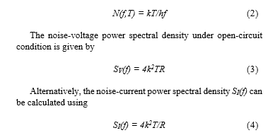
Figure 1 (a) and (b) show the Johnson noise of NP-CdS:P3HT and NP-CdSe:P3HT, respectively. The unexposed film has the greatest resistance expressed as the highest noise level compared to the films exposed to H2S or H2Se gas environment.
The unexposed films are highly resistive due to the presence of stearic acid in the P3HT matrix. Stearic acid hinders efficient electrons movement. However, exposure of the thin film to H2S or H2Se gas, causing nanoparticles to nucleate in between P3HT layers. These nanoparticles facilitate the flow of electron, thus lowering the spectral density of noise. The high noise fluctuation for NP-CdS:P3HT thin film indicates that there could be an aggregation of the charges resulting in more substantial resistance at high frequency [21].
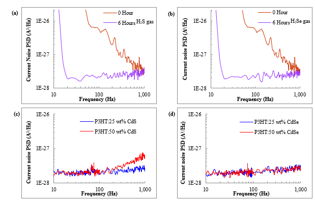 Figure 1: Johnson noise current spectral density of (a) NP-CdS:P3HT (b) NP-CdSe:P3HT (c) QD-CdS:P3HT (d) QD-CdSe:P3HT
On the other hand, as shown in Figure 1 (c) and (d), QD-CdX:P3HT has lower Johnson noise as compared with NP-CdX:P3HT thin films. Among the benefits of thin films formed by directly combining quantum dots with P3HT is that both elements are an exceptional conductor. Therefore the noise for this device is substantially low and stable irrespective of the amount or types of quantum dots. Nonetheless, QD-CdX:P3HT thin films display a growing increase in noise spectra at a frequency greater than 100 Hz, suggests that the thin film is prone to high-frequency degradation.
The noise results were supported by current density-voltage (J-V) measurement. The electrical properties studied were open-circuit voltage (Voc), short-circuit current density (Jsc), fill factor (FF), and maximum power output (Pmax). The fourth quadrant of J-V graphs for NP-CdX:P3HT thin films under illumination were plotted in Figure 2. Excitons are created when incident photons are absorbed in thin films. Then, the excitons dispersed inside the polymer matrix until they reached the interface between polymer/nanoparticles and disassociated into electrons and holes [22]. Consequently, the electric field formed at the boundary layer, pushing electrons and holes to the opposite sides. The nanoparticle’s HOMO and LUMO energy is relatively lower than P3HT. The electrons will then be transported to the cathode while the holes are transferred to the anode, producing photocurrent [23].
The thin films exposed to the gas environment demonstrated greater Jsc as compared to film not treated with gas. When no current is supplied or J = 0 A, Voc can be determined. Figure 2 demonstrated that the value of Voc for the exposed films was twice as large as compared with unexposed thin films. NP-CdSe:P3HT gives the highest Voc , 0.72 V, while the other films are in the range of 0.2 – 0.6 V. Even the principle of Voc is not yell well known, Brabec et al. suggest that it depends heavily on the ionization potential of the donor and the electron affinity of the acceptor; hence the amount energy offset [24]. Meanwhile, Qi et al. show Voc is determined by the composition of the elementals’ mixture even it is not a straightforward relationship [25]. Thus it justifies the low Voc value for thin films before gas treatment due to underdeveloped nanoparticles nucleation in the film matrices.
Short-circuit current density, Jsc, occurs when the current flow through the external circuit without connecting to a voltage source, V = 0 V. Low Jsc value for entire samples imply limited photon absorption by the films. Transportation of the charge is associated with Fill Factor or FF. High charge mobility is desired to prevent significant losses due to recombination [26, 27]. However, calculation shows FF values are small for all samples indicating the considerable recombination level occurs in thin films. The results are as corroborated by low Jsc value. The “squareness” of the FF is contributed by maximum power output, Pmax, that is when the current and the voltage of the device are at maxima, or:
![]()
where VMPP and JMPP are the values of voltage and current density at the maximum power point (MPP). Electronic devices must be operated at the maximum power point to generate maximum energy efficiency and minimize losses. In order to achieve maximum energy performance and, at the same time, reduces losses, the electronic appliances are desired to be operated at the highest power point [28].
The exposure of H2S or H2Se gas nucleated approximately 9% of nanoparticles. Hence the improvements in Pmax for the exposed film were insignificant. Thin films mixed with 50 wt% quantum dots, however, posses even smaller Pmax value. This is contrary to the study by Lek et al. that reports a rise in the weight ratio of nanoparticles would improve electrical performance [29]. Nonetheless, the improvement can only be observed until a certain weight percentage is reached. Whilst the study shows a low amount of quantum dots or nanoparticles causes inefficient pathways for electrons transportation [30], too high nanomaterials loading causing limited mobility of the holes, leading to lower device’s performance. The summary of the J-V analysis is as tabulated in Table 1. The overall results demonstrated that NP-CdSe:P3HT nanocomposite the most reliable performance in both Johnson noise and J-V evaluation of all thin films.
Table 1: The electrical properties of thin films from J-V measurement
| Voc (V) |
Jsc (mA/cm2) |
FF |
Pmax (mW) |
|
| NP-CdS:P3HT | 0.2 | 1.2 × 10⁻³ | 0.18 | 1.2 × 10⁻⁴ |
| NP-CdSe:P3HT | 0.72 | 1.2 × 10⁻³ | 0.15 | 1.3 × 10⁻⁴ |
| QD-CdS:P3HT | 0.32 | 1.1 × 10⁻⁴ | 0.14 | 4.8 × 10⁻⁶ |
| QD-CdSe:P3HT | 0.2 | 7.5 × 10⁻⁵ | 0.21 | 3.2 × 10⁻⁶ |
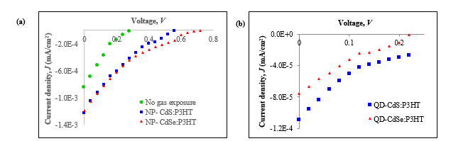 Figure 2: J-V graphs for thin films (a) unexposed sample, sample exposed to H2S gas (NP- CdS:P3HT) and H2Se gas (NP-CdSe:P3HT), and
(b) QD-CdS:P3HT and QD-CdSe:P3HT
Figure 3 (a) displays the absorption spectra of pristine P3HT thin film, thin films before gas exposure, and after exposure to H2S gas and H2Se gas. Conjugation system in P3HT causes two peaks at 522 and 556 nm and a shoulder at 605 nm to appear in the UV-Vis graph. A similar result has been obtained by the Liao research group [31]. The peaks attribute to π-π* transition or the order of intermolecular chains of the polymer, while the shoulder is due to crystallization of polymer [32, 33]. When P3HT were mixed with stearic acid, the absorption spectra are lower than that of pristine P3HT, and its peak shifted towards the red spectrum at 529 and 560 nm, and the shoulder becoming less distinguishable. The shift indicates the presence of Cd2+ ion capped in the stearic acid matrices, as well as reduced P3HT π-conjugation length.
Before the thin films were exposed to the gas, the observable peak is at 560 nm. Nonetheless, exposure to H2S gas environment for 6 hours caused the peak to shift to 556.5 nm. The blue shift of the peaks inkling the quantum confinement effect due to CdS nanoparticles formation in the thin film [34, 35]. The shoulder at 605 nm is more perceptible compared with an unexposed thin film. This shoulder is usually due to an increased crystallization of intra-chain interactions. The exposure to H2S gas causing the absorption intensity to become lesser. This is due to the reaction of cadmium stearate with H2S gas:
![]()
Similar to H2S gas exposure, the absorption intensity of thin films exposed to H2Se gas ambiance decreased compared with the unexposed thin film. One possible reason that contributes to such a profile is the shape and amount of CdSe nanoparticles created. The aspect ratio of CdSe nanoparticles is high, in which it resembles rod-like, and some of the nanoparticles agglomerate, creating a larger cluster.
Photoluminescence (PL) is a process of spontaneous light emission from the material under optical excitation. Ideally, the PL spectrum mirroring the image of the absorption spectrum, hence it clearly can be observed from Figure 3(b) the PL spectra resemble the UV-Vis absorption spectra. PL measurement is an indicator of excitons dissociation and its efficiency to transfer charge in the composite materials. The intensity of PL decreased when exposed to H2S and H2Se gas. The gas exposure caused the peak shifted towards the blue region, from 720 nm to 718 nm and 714 nm, respectively. The deviation suggested the reduction in P3HT aggregation, causing the PL to quench.
The occurrence of PL depends on the distance from the excitons formed to the donor/acceptor interface [36]. If the distance is lesser than the excitons’ diffusion length, charge transfer to the nanoparticle is anticipated, hence the PL is quenched [37]. The more significant range caused recombination to take place. From literature, exciton diffusion length for P3HT is around 8 nm [38]. However, FESEM images in Figure 3 (c) – (e) showed that the distance between nanoparticles was considerably large, ranging from 100 to 150 nm. The number of nanoparticles impregnated in the thin film was small, causing the exciton that is further from the donor/acceptor interface to recombine before reaching the interface.
The UV-Vis spectra when the CdS / CdSe quantum dots were physically mixed into P3HT polymer as shown in Figure 4 (a) and (b). The absorption of pristine P3HT is comparable to the thin film with 25 wt% CdS and CdSe QDs. However, for QD-CdS:P3HT, the absorption is lower when the amount of QDs is doubled. This may be due to a smaller amount of P3HT in the composite [39]. The peaks and shoulders remain at the same wavelength as pristine P3HT. The absence of the CdS QDs absorption band is likely due to the overlapping with the P3HT absorption. While at 50 wt% of CdSe, the absorption is higher, and the shoulder is less distinguishable. The peaks are poorly shifted to red, 524 and 557.5 nm indicating the polymer chains are less crystallized due to QDs added. Both QD-CdS:P3HT and QD-CdSe:P3HT show no significant in amplitude variation with the increment of QDs wt%, comparable to the results reported for P3HT:CdSe TBPO-capped at different weight percentage [40].
 Figure 3: (a) UV-Vis absorption spectra, (b) photoluminescence spectra and (c) FESEM images for thin films not exposed to any gas,
(d) exposed to H2S gas (NP- CdS:P3HT), and (e) H2Se gas (NP-CdSe:P3HT)
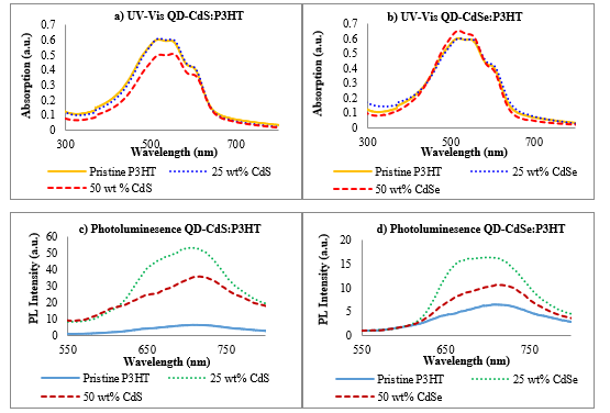 Figure 4: UV-Vis absorption spectra and photoluminescence of QD-CdS:P3HT and QD-CdSe:P3HT
On the other hand, photoluminescence spectra for QD-CdS:P3HT and QD-CdSe:P3HT are shown in Figure 4 (c) and (d), respectively. Both types of thin-film displayed similar characteristics, in which a higher amount of QDs (50 wt%) mixed into P3HT cause the film to quench stronger as compared to films with 25 wt% QDs. The quenching indicates a reduction in the domain size of P3HT blended with nanoparticles [41]. The decrease is owing to a shorter distance for the excitons to travel to the donor/acceptor interface when the weight percentage of nanoparticles in the polymer is doubled. The PL quenching also possibly due to the π-π interaction of P3HT with the nanoparticles [42], creating a new decaying pathway for excitons [43]. Higher excitons dissociation can be justified for better device performance.
Nonetheless, the PL intensity of P3HT:CdS QDs is higher and has a narrower peak than that of P3HT:CdSe QDs. The P3HT:25 wt% CdS has a maximum at 704 nm, while for P3HT:50 wt% CdS, the peak shifted to longer wavelength, 713.5 nm. The shift is also known as Stokes-shift. The redshift implies the increment in polymer aggregation, which can be achieved by the incorporation of QDs into the polymer matrix, as have also been observed by others [44].
4. Conclusion
The analysis has been done on the nanocomposite thin films prepared via two approaches – direct impregnation of nanoparticles in P3HT matrix (in-situ), and by physically mixing quantum dots with P3HT (ex-situ). Results show that QD-CdX:P3HT thin films possess low Johnson noise due to intrinsic properties of quantum dots and P3HT as an excellent conductor. Consequently, the noise is considerably small and stable for this system regardless of the weight percentage or types of quantum dots. However, the increment of noise can be observed at a frequency above 100 Hz for QD:CdX-P3HT thin films. This signifies the thin film is vulnerable to high-frequency degradation. For nanocomposite produced through the in-situ technique, the presence of stearic acid the P3HT matrix curb the free flow of electrons movement.
It can be concluded NP-CdSe:P3HT nanocomposite displayed more reliable performance in both Johnson noise and J-V measurement. Absorbance spectra show higher polymer crystallization NP-CdX:P3HT. The quantum confinement effect due to nanoparticles formation is translated by the shift of peaks and depreciation of absorption intensity. The PL intensity decreased when exposed to the gas. Both the thin films fabricated ex-situ displays similar spectra profile even when the amount of quantum dots was doubled. While the amount of quantum dots did not affect the absorbance significantly, the PL intensity decreased with increment of quantum dots’ weight percentage. Overall, NP-CdX:P3HT showed better performance compared to QD:CdX-P3HT nanocomposite. Such findings have provided a bright prospective to study the nucleation of nanoparticles through gas exposure technique for optoelectronics applications.
Conflict of Interest
The authors declare no conflict of interest.
Acknowledgment
Authors are grateful to Universiti Putra Malaysia for the financial support through IPM Putra research grant 9674000.
- Y. J. Park, H. S. Cho, “An experiment of human presence and movement using impulse radar and machine learning”, 2019 International Conference on Information and Communication Technology Convergence (ICTC), 2019, doi:10.1109/ICTC46691.2019.8939858.
- J. Kwon, S. Lee, N. Kwak, “Human detection by deep neural networks recognizing micro-doppler signals of radar”, in 15th European Radar Conference (EuRAD), 26-28, 2018, doi:10.23919/EuRAD.2018.8546605.
- L. Ren, Y. S. Koo, Y. Wang, A. E. Fathy, “Noncontact heartbeat detection using UWB impulse Doppler radar”, in Proceedings of the IEEE Topical Conference on Biomedical Wireless Technologies, Networks, and Sensing System, 14–16, 2015, doi:10.1109/BIOWIRELESS.2015.7152128.
- R. J. Fontana, “Recent system applications of short-pulse ultra-wideband (UWB) technology”, IEEE Trans. Microw. Theory Tech., 52, 2087-2104, 2004, doi:10.1109/TMTT.2004.834186.
- V. H. Nguyen, J. Y Pyun, “Location detection and tracking of moving targets by a 2D IR-UWB radar system”, Sensors 15(3):6740-62, 2015, doi:10.3390/s150306740.
- Novelda, NVA620x Preliminary Datasheet, Novelda AS, Oslo, Norway, 2013.
- Y. J. Park, H. S, Cho, “Detecting human movement during vital sign measurement using heterogeneous sensors”, ITC-CSCC2019, 2019, doi:10.1109/ITC-CSCC.2019.8793461.
- V. Jakkula, “Tutorial on Support Vector Machine (SVM)”, School of EECS, Washington State University, Pullman 99164.
- Tutorial slides by Andrew Moore. http://www.cs.cmu.edu/~awm
- C. Burges, “A Tutorial on Support Vector Machines for Pattern Recognition”, Data Mining and Knowledge Discovery, Kluwer Academic Publishers, 2, 121-167, Boston, 1998, doi: 10.1023/A:1009715923555.0.
- N. Cristianini, J. Shawe-Taylor, “An Introduction to Support Vector Machines and other Kernel-based Learning Methods”, Cambridge University Press, 2000, doi:10.1017/CBO9780511801389.
- J. P. Lewis, Tutorial on SVM, CGIT Lab, USC, 2004.
- Tutorial slides by Andrew Moore. http://www.cs.cmu.edu/~awm
- M. Sewak, Md. R. Karim, P. Pujari, “Practical Convolutional Neural Networks – GoogLeNet architecture”, 2018, https://subscription.packtpub.com/book/data/9781788392303/4/ch04lvl1sec31/googlenet-architecture.