
Efficiency Enhancement of p-i-n Solar Cell Embedding Quantum Wires in the Intrinsic Layer
Volume 5, Issue 3, Page No 540-546, 2020
Author’s Name: Nahid Akhter Jahan1, M. Mofazzal Hossain2,a)
View Affiliations
1Department of Electrical and Electronic Engineering, Southeast University, Dhaka 1212, Bangladesh
2Department of Electrical and Electronic Engineering, University of Liberal Arts Bangladesh, Dhaka 1209, Bangladesh
a)Author to whom correspondence should be addressed. E-mail: mofazzal.hossain@ulab.edu.bd
Adv. Sci. Technol. Eng. Syst. J. 5(3), 540-546 (2020); ![]() DOI: 10.25046/aj050367
DOI: 10.25046/aj050367
Keywords: Quantum wire, Solar cell, Conversion efficiency, InAs/GaAs, Simulation

Export Citations
A high efficiency InAs/GaAs quantum wire solar cell is modelled embedding periodic array of InAs quantum wires (QW) in the intrinsic layer. The promising low dimensional heterostructure such as Quantum Wells, Quantum Wires, Quantum Dots or Dashed (elongated Dots) based intermediate-band-gap solar cells are recently being grasped the attention for ongoing third generation solar cell studies. In this particular work, we contrive, design and thereby simulate the solar cell incorporating QWs with a view to magnify the efficiency. After implementation of 15 layers of InAs QWs conjugated within the intrinsic layer and with the adaptation of AM1.5 solar irradiance, the proposed cell structure ensued a Voc of 1.26 V, Jsc of 32.83 mAcm-2 and a fill factor of 89.4%, which eventuates an overall cell efficiency of 37%. We achieved an efficiency of 26.98% with the same materials and dimensions without QWs in intrinsic layer. Therefore, it may be optimistically appealed that the insertion of QWs in the intrinsic layer has an affirmative impact on the efficiency of the cell.
Received: 22 May 2020, Accepted: 14 June 2020, Published Online: 25 June 2020
1. Introduction
It cannot be over-emphasized that the want for the development of sustainable energy sources are becoming paramount as the ubiquitous demand for energy supply is ever increasing with the constraint or the limitation of fossil fuel reserves which is indeed exhaustible. Our fixation for fossil fuels date back to industrial revolution and the unbridled consumption of these fuels, have been deliberately forgoing the earth toward climatological cataclysm. In many ways, we ceaselessly pushing our planet’s terrestrial in catastrophic debacle and whacking the earth’s eco-system by these fuel’s burning. Eventually, we ended up making an ozone contraction, causing our climate an ever-hotter with ever-rising sea levels, a toxic muddle of nature, recurrent droughts, and alarming global crisis all owing to the gushing of lethal greenhouse gases (GHG) and air pollutants ensued from combustion of fossil fuels [1]. Therefore, there is no gainsaying the fact that we instead must start switching to non-pollutant sustainable sources of renewable energy and the scientists from all over the world are reiterating the world-leaders to patronize the technologies of non-polluting green-energy harness. Corollary, for combating this staggering climate crisis, solar photovoltaic (PV) cells have been prevalently considered as one of the most promising sustainable green-energy technologies. Depending on the underlying technology, PV cells can be categorized into three generations. The first-generation PV is based on single or multi-crystalline silicon p-n junction cells. Second-generation solar cells are called thin-film solar cells as the semiconductor materials are only a few micrometers thick. However, for single junction solar cells either first- or second-generation, the thermodynamic efficiency limit of sunlight to electric power conversion efficiency (η) is 32.9% [2]. This limitation is well known as the Shockley-Queisser limit [3] which states that the photons with energies less than the bandgap energy are not absorbed and also the photons with energies greater than the bandgap energy release the additional energy in the form of heat which eventuates into thermalization loss. Therefore, the aim of third-generation solar cells is to achieve conversion efficiency which will surpass the Shockley-Queisser limit [4]. In this context, low dimensional hetero-structures (nano-structures), such as Quantum Wells (QWL), Quantum wires (QW), Quantum dots (QD), and elongated Quantum dots (Quantum dash) based solar cells have shown very promising prospect to achieve this expectation. It is worth stating that the QWL assures confinement of excitons in 1-dimension, whereas the QW assures s confinement of exciton in 2-dimension and QDs/dashes establish confinement in all 3-dimensions. Theses nano-structures, specially QW, and QDs exhibit outstanding opto-electronic properties owing to their ability to create veritable confinement with discrete and disparate energy states above the energy gaps of the bulk constituents [5-7].
They possess a unique property that is by changing the diameter of the QDs one can actually modulate their bandgap (the exciton energy-gap) which provides tunability of absorption spectrum [8]. It is seen that as the quantum diameter decreases, the breach or separation between the energy level increases. In line with this, it has been observed that as the separation between adjacent QDs or Quantum dashes is reduced, it results in the formation of coupled confined exciton states among these nano hetero-structures and thereby acts as a channel of charge-carriers transfer from high exciton-energy QDs to low exciton-energy QDs [9, 10]. All these phenomena establish that the exciton-bandgap and the dynamics of charge carriers are the function of size, proximity and positioning for all these QWL, QW, and QDs. Because of these properties, fabricating or positioning of QWL, QW, and QDs inside a semiconductor renders these structures as one of the potential candidates for realizing intermediate band solar cells (IBSCs) [11] as their discrete energy states act exactly like intermediate band (IB). IB utilizes sub-bandgap absorption which can thereby generate additional photocurrent from low-energy photons of the solar spectrum [4,12]. Convinced by this suitability of QDs, the p-i-n InAs/GaAs quantum dot embedded solar cell model was first modelled and proposed by [13]. In his model, by inserting QDs in intrinsic region the cell efficiency was increased from 19.5% (without QDs) to 25%. Since then quite a lot of studies have been done on InAs/GaAs QD solar cells to improve its efficiency compared to GaAs solar cells using the same structure [14-19]. Those reports demonstrate the achievement of circa 17% conversion efficiency in InAs/GaAs QD solar cell containing five stacks of QDs in intrinsic (i)-region by doping the InAs QDs with Si during the fabrication process.
In this work, we particularly intended to study the effect of Quantum Wire (QW) on the performance of intermediate band solar cell (IBSC). We investigated the plausible chance of increasing the efficiency of InAs/GaAs QW embedded intermediate band solar cell (IBSC) by stacking multiple InAs QW layers within the intrinsic layer. The modelling and simulation was performed using Silvaco TCAD software. Initially, the simulation was conducted without QWs in the intrinsic layer with an intention to compare this structure with the structure of similitude including QWs in intrinsic layer (InAs QWs buried in intrinsic-layer). Thereafter, secondly we carried out the simulation of InAs/GaAs QWs embedded p-i-n solar cell in the same software and adopting similar dimensions of the cell as above.
Here, we will depict our analysis and comparison between the results that upholds our insinuation and expectancy of efficiency enhancement for the structure having QWs inside. The associated design-calculation of band structure by determining exciton-confinement energies of InAs/GaAs QW is quantitatively performed and thereby included to corroborate our interpretation of the results. We, therefore, present an approach and deliver the proof to state that solar cell with Quantum Wires in the intrinsic region indeed improves the cell efficiency conceivably by capturing multiple photons through multiple discrete excitons states encompassing wider range of solar spectrum.
2. Structure and Modeling of p-i-n InAs/GaAs QW Solar Cell
2.1. Schematic Elucidation of the Proposed p-i-n InAs/GaAs QW Solar Cell
The schematic structure of proposed p-i-n InAs/GaAs solar cell is depicted precisely in Figure 1. In this structure of QW embedded p-i-n solar cell, we used GaAs as n-type (3.1 mm thick) and p-type (540 nm thick) layers at the top and bottom of the intrinsic region (112 nm thick) respectively and multiple layers of InAs QWs are buried or sandwiched within the GaAs barriers in the intrinsic region. Figure. 1 is an exemplar of 7-layers of QWs. The dimension of the InAs QW has a height of 5 nm with a width of 10 nm and the spacing between adjacent QWs are kept 10 nm throughout. The barrier height of GaAs beneath the InAs QW is chosen as 6.5 nm and the barrier height of GaAs as capping above the QW is chosen as 4.5 nm. The total thickness of each InAs QW embedded inside the GaAs-barriers (InAs QWs/GaAs-Barriers) becomes 16 nm (6.5 nm + 5 nm + 4.5 nm). The collective thickness of intrinsic layers becomes 112 nm (16 x 7 nm) for 7-layers of InAs QWs/GaAs-Barriers. The Aluminum and Molybdenum are used as anode and cathode, respectively, where the length of Aluminum is specified as 20 nm. Owing to the opacity of Aluminum, the active solar insolation region is quantified as 80 nm as seen in the Figure. 1. Therefore, each embedded layer of InAs QWs is comprised of four periodic QWs alongside. Furthermore, a highly doped p+ layer of 200 nm thick InGaP is introduced amid the back contact and the 540 nm thick p-type GaAs which is called the back-surface field (BSF) layer. BSF layer is commonly introduced to reduce the loss due to recombination and thus enhancing the conversion efficiency. At the very top of the solar cell, 498 nm thick ZnO is used as a transparent conductive oxide (TCO) layer to reduce the series resistance of the cell that mostly results from our thick n-type window layer, thereby increasing the open circuit voltage. Eventually, the net thickness of the semiconductor (p-i-n) becomes 3.852 mm, whereas including TCO-layer the net thickness becomes 4.35 mm. It is worth noting that, in the window layer a wider band-gap of 50 nm thick n-type InGaP (1.8 eV at 300 K) is inserted with a plausible chance of achieving meteoric rise in the absorption of higher energy photons even above the GaAs energy-gap (1.43 eV at 300 K) limit. For simplicity, during simulation, the top and bottom contacts are assumed to be Ohmic rather than Schottky.
The energy band diagram of the proposed p-i-n InAs/GaAs QW solar cell is illustrated in Figure 2 from which a comprehensive understanding of the operation of the proposed p-i-n InAs/GaAs QW solar cell is possible. Although practically the conduction and valance band offsets between barrier and QWs are not equal, however, for simplicity we sketched the band diagram considering the band offsets same for both conduction and valance band region. The effects of strain on the valance band has been neglected for this consideration. The engineering of energy band diagram at the intrinsic region due to the incorporation of QWs as low dimensional structure will ensure more effective utilization of solar spectrum, wherein photons matched with multiple confinement energies of different sized QWs will be effectively absorbed. In this way it will be possible to utilize the wider range of solar spectrum for efficient conversion in comparison with typical single junction solar cells. Thereby this proposed structure is credibly suitable to overcome the Shockley-Queisser limit. The calculation of 1-dimensional (1-D), 2-dimensional (2-D) exciton energies and band-diagram for 1-D confinement of InAs/GaAs QW hetero-structure is represented in the next sub-section.
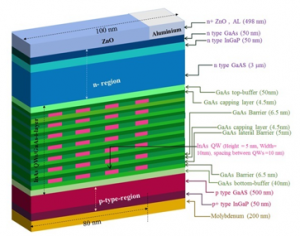
Figure 1. Structure of the proposed p-i-n InAs/GaAs QW solar cell
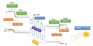
Figure 2. Energy band diagram of proposed p-i-n InAs/GaAs QW solar cell
Figure 3 (a) shows the proposed structure of InAs/GaAs QWs embedded solar cell generated in Silvaco environment. The zoomed-in view of InAs QW layers inside the intrinsic region produced in Silavaco is also shown in Figure 3 (b). The information regarding the dimension of QWs and buffer layers is illustrated in Figure 3 (c). In this structure we considered 15 layers of similar sized QWs. For all of our simulated structures including QWs, the dimension of each QW is consistently kept 10 nm×5 nm. The doping concentrations of n+ , n, p, and p+ regions have been assumed as 2.5×1020 cm-3, 1×1018 cm-3, 1×1017 cm-3, and 2×1018 cm-3 respectively.
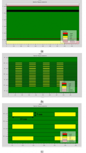
Figure 3. (a) Structure of InAs/GaAs QW solar cell (x-axis and y-axis dimension are in microns) generated in Silvaco, (b) The zoomed-in view of 15 layers of QDs in intrinsic region generated in Silvaco, and (c) The extended zoomed-in view for observing the size of InAs QWs in intrinsic region (x-axis and y-axis dimension are in microns)
2.2. Calculation of Exciton Energies and Construction of Band-Diagram for 1-D Confinement of InAs/GaAs QW Hetero-Structure
For comprehensive understanding of the formation of intermediate energy bands, confinement energies of excitons (electrons and hole pair) in InAs QW have been calculated by solving the Schrödinger equation for finite-potential barriers (GaAs-barriers on both side of QW). Our calculated exciton energies (for one dimensional confinement) are illustrated in Figure 4 and summarized in Table: 1 for different thickness of QWs. Relied on the accessible evidence, the QW confinement-energies calculation have been performed from the solution of the empirical Schrödinger equation by assuming the conduction band offset as 70% (or valence band offset of 30%) [20].
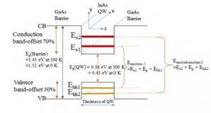
Figure 4. Calculated ground state and excited states confinement energies of excitons (Electron-hole pairs) and construction of energy-band-diagram for 1-dimensional confinement of InAs/GaAs QW hetero-structure
The physical pertinent parameters, e.g., energy bandgap, electron and heavy hole effective masses, the lattice constant, the magnitudes of stiffness constants, and deformation potentials for strain calculation were all adopted from the established values for InAs and GaAs [21]. The associated equations and details of this calculation can be found in our previous work performed for InGaSb/AlGaSb Quantum Well [22]. For most of the cases III-V hetero-structures such as for InAs/GaAs, the band offset is nearly localized to the conduction band. In this case, for confinement energies calculation and band structure development, we assumed the valence band offset as 30%. This lesser valance band offset is analogous to the formerly published standards [20]. It is to be noted that for the case of InAs/InP hetero-structures, the band offset is nearly equally distributed to the both bands (conduction and valence), whereas the band offset is found mostly contained to the conduction band (87%) in our previous study of antimony based Quantum Well [22].
As we can see that for a QW of height 5 nm, the ground-state exciton energy at 0 K is achieved as— Eexciton-1 = Ee1 + Eg(QW) +Ehh1= 774 meV. At 300 K the ground-state exciton energy will be reduced to Eexciton-1 = 704 meV, because of the temperature dependent bulk Eg of InAs (360 meV at 300 K). Whereas for a QW of 10 nm thick, the ground-state exciton energy at 0 K is determined as— Eexciton-1 = Ee1 + Eg(QW) +Ehh1= 552 meV, and at 300 K this exciton energy will be reduced to Eexciton-1 = 482 meV. Alongside the calculation ensued the excited-state exciton energy as— Eexcited–exciton-2 = Ee2 + Eg(QW) +Ehh2= 1026 meV at 0 K, and 956 meV at 300 K. Where, Ee1 is the energy of ground-state electron confinement, Ehh1 is the energy of ground-state heavy-hole confinement, Ee2 is the energy of excited-state electron confinement, Ehh2 is the energy of excited-state heavy-hole confinement, and Eg (QW) is the energy gap of InAs. (Since the strain contribution for InAs/GaAs is not more than a few meV, it has been neglected).
In our proposed structure, the dimension of our QW is selected as 10 nm × 5 nm (width in y × thickness in z). Therefore, the confinement is assured in 2-dimensional, i.e. the exciton is confined in both y and z direction while along the x-direction is free. Thus the total ground-state exciton energy will be — Eexciton-1 (2-D confinement) = Ee1(z) + Ee1(y) + Eg(QW) + Ehh1(z) + Ehh1(y) =(307 + 112 + 360 + 37 + 10) = 826 meV. If we subtract the exciton binding energy of InAs (1.8 to 2 eV [23], the resultant
Table 1: Electron and heavy-hole confinement of InAs/GaAs
|
Thickness of QW, Lz (nm) |
Ee1 (meV) |
Ee2 (meV) |
Ehh1 (meV) |
Ehh2 (meV) |
Eg (QW) (meV) At 0 K |
Eg (QW) (meV) At 300 K |
Eexciton1 =(Ee1+Ehh1+Eg(QW)) (meV) at 0 K |
Eexciton1 =(Ee1+Ehh1+Eg(QW)) (meV) at 300 K |
Eexcited-exciton2 =(Ee2+Ehh2+ Eg(QW)) (meV) at 0 K |
Eexcited-exciton2 =(Ee2+Ehh2+ Eg(QW)) (meV) at 300 K |
| 2 | 598 | 164 | 430 | 360 | 1192 | 1122 | ||||
| 2.5 | 541 | 122 | 430 | 360 | 1093 | 1023 | ||||
| 3 | 486 | 92 | 430 | 360 | 1008 | 938 | ||||
| 3.5 | 434 | 71 | 430 | 360 | 935 | 865 | ||||
| 4 | 387 | 56 | 430 | 360 | 873 | 803 | ||||
| 4.5 | 345 | 45 | 430 | 360 | 820 | 750 | ||||
| 5 | 307 | 37 | 430 | 360 | 774 | 704 | ||||
| 5.5 | 274 | 31 | 430 | 360 | 735 | 665 | ||||
| 6 | 245 | 27 | 430 | 360 | 702 | 632 | ||||
| 6.5 | 220 | 763 | 23 | 118 | 430 | 360 | 673 | 603 | 1311 | 1241 |
| 7 | 198 | 753 | 20 | 103 | 430 | 360 | 648 | 578 | 1286 | 1216 |
| 7.5 | 179 | 727 | 17 | 91 | 430 | 360 | 626 | 556 | 1248 | 1178 |
| 8 | 162 | 694 | 15 | 81 | 430 | 360 | 607 | 537 | 1205 | 1135 |
| 8.5 | 147 | 660 | 14 | 72 | 430 | 360 | 591 | 521 | 1162 | 1092 |
| 9 | 135 | 624 | 13 | 63 | 430 | 360 | 578 | 508 | 1117 | 1047 |
| 9.5 | 124 | 586 | 12 | 54 | 430 | 360 | 566 | 496 | 1070 | 1000 |
| 10 | 112 | 550 | 10 | 46 | 430 | 360 | 552 | 482 | 1026 | 956 |
Eexciton-1 (2-D confinement) becomes 824 meV which is equivalent to 1500 nm of wavelength. Similarly the total excited-state exciton energy will be — Eexcited–exciton-2 (2-D confinement) = Ee2(z) + Ee2(y) + Eg(QW) + Ehh2(z) + Ehh2(y) =(0 + 550 + 360 + 45 + 0) = 953 meV. Subtraction of exciton binding energy for excited states can be eliminated, because exciton in ground state are more confined than that of the excited states. From the aforementioned analysis it can be inferred that the proposed structure of QW provides an intermediate band (IB) of energies from 826 to 956 meV in the i-layer of p-i-n diagram, which corresponds to a wavelength range of 1290 to 1500 nm. Therefore, our QW-based IBSC can afford multiple lower-energy photons absorption covering this wavelength range (1290-1500 nm) of insolation together with the absorption of higher-energy photons in p and n-GaAs/InGaP of window and base layers. Typically, the maximum photons that can be absorbed by GaAs is around 875 nm [24] and by InGaP is around 688 nm.
3. Results and Discussion
In this work, we considered a one-sun solar irradiance of AM 1.5 for simulation. At first the simulation was carried out for p-i-n solar cell without QWs and achieved an efficiency of 26.9%. Then, simulation was further carried out to investigate the effects of stacking multiple layers of InAs quantum wires in the intrinsic region and to find out how it impacts the conversion efficiency for this proposed cell. For this purpose, the simulation is conducted particularly for three distinct cases; structure’s having 7, 10 and 15-layers of QWs in the intrinsic layers. Table 2 shows the simulation results which include the density of short circuit current (JSC), open circuit voltage (VOC), fill factor (FF), and conversion efficiency (η).
Table 2: Characteristic parameters of InAs/GaAs solar cell for various number of QW layers
| Number of QD layers | (mA/cm2) | (Volts) |
FF (%) |
η (%) |
| 0 | 28.2 | 1.08 | 88.4 | 26.9 |
| 7 | 32.2 | 1.26 | 89.4 | 36.3 |
| 10 | 32.5 | 1.26 | 89.5 | 36.6 |
| 15 | 32.9 33 | 1.26 | 89.4 | 37 |
Now if we compare and analyse the simulation results presented in Table 2, it can be realized that with the increasing number of embedded QW layers inside the intrinsic region the short circuit current density increases, which ultimately indicates the generation of additional excitons (electron-hole pairs). However, with the increasing number of QW layers the open circuit voltage remains completely constant. This is very likely and expected because the upper limit of open circuit voltage predominantly depends on the energy gap, band offsets of the QWs/barriers and the confinement energies of QWs, not on the surplus creation of excitons. Figure 5 shows the current density vs voltage curve of InAs/GaAs quantum dot solar cell exemplarily for 0 and 15 layers of QWs. When comparing the short circuit current densities of InAs/GaAs solar cells without QWs and with 15 layers of QWs, it is found that there is a relative augmentation of about 16.2%.
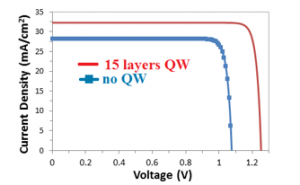
Figure 5. Current density vs voltage characteristics of InAs/GaAs QWSC (QWs layers = 0, 15)
The conversion efficiency of a solar cell indicates the probability that an incident photon would generate an exciton (electron-hole pair). With the increasing number of quantum dot layers in the intrinsic region, the conversion efficiency significantly increases as shown in Figure 6. For InAs/GaAs QW solar cell, 37% conversion efficiency is achieved for 15 layers of QWs whereas for InAs/GaAs solar cell without QWs it is only 26.9%. As we quantitatively calculated the exciton energies and band-diagram for 1-D confinement of InAs/GaAs QW hetero-structure in our previous section (b. sub-section of section 2), we observed that the proposed structure of QW can afford an intermediate band (IB) of energies from 826 to 956 meV in the i-layer, which corresponds to a range of wavelength 1290 to 1500 nm. Thereby it can absorb multiple lower-energy photons covering this wavelength range (1290-1500 nm) of light together with the absorption of higher-energy photons by the window and base layers (GaAs and InGaP). As previously discussed, low dimensional hetero-structure-based solar cells are considered to be a promising candidate in mimicking the characteristics of intermediate band solar cells. The advantage of using QW in the intrinsic region is the absorption of lower energy photons having longer wavelengths which eventually leads to greater conversion efficiency. For a typical GaAs solar cell, the maximum photons that can be absorbed is around 875 nm [24]. Also owing to the inclusion of InGaP in both n and p-regions ensures photons absorption in around 688 nm. Compared to a typical GaAs solar cell the absorption range would be much wider for this QW solar cell due their ability to absorb even lower energy photons. From our analysis, it can be inferred that, our proposed quantum dot embedded structure is indeed helpful for the realization of solar cells to absorb photons with lower energy having wavelengths from 1290 nm to 1500 nm.
The simulation is also conducted to study the effects of thickness of n-type window layer on the cell efficiency while the thickness of all the other layers remained unchanged as shown in Figure 1. It is evident from Figure 7 that there is an almost linear increase in conversion efficiency with the increase in thickness of n-type window layer. This phenomenon can be understood by the fact that larger the n-layer thickness smaller the series resistance of the cell. However, it is noticed that when the thickness of n-type window layer is increased from 2 µm to 4 µm, the conversion efficiency increases insignificantly. Moreover, the effect of concentration of n-type window layer on efficiency is also studied. Figure 8 depicts the effects of dopant concentrations in the n-type window layer and it is observed that there is a very negligible increase in conversion efficiency with an increase in dopant concentration.
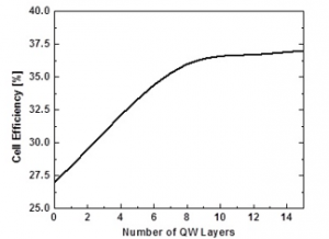
Figure 6. Evolution of cell efficiency with the number of QW layers
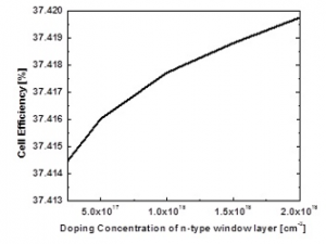
Figure 7. The dependence of Cell efficiency on the thickness of n-type window layer
Figure 8. Evolution of cell efficiency with the dopant concentration of n-type window layer
4. Conclusion
InAs/GaAs solar cell is a distinctive example of III-V hetero-structure to achieve higher conversion efficiency thereby can be considered as one of the prospective candidates for the realization of solar cell having greater performance. By embedding QWs in the intrinsic region, higher conversion efficiency for third generation solar cell can be realized. In this work, the impacts on the characteristic parameters of a solar cell due to the insertion of stacked QW layers in the intrinsic region are studied. We proposed 7 to 15-layers of QWs based solar cell structure that reveals the highest reachable conversion efficiency of 37% whereas p-i-n solar cell without QWs shows a conversion efficiency of only 26.9%. The insertion of QWs in the intrinsic region improves the photon absorption range by absorbing lower energy photons in the IB having longer wavelength from 1290 nm to 1500 nm. However, the technical limitation of this work is that the achieved conversion efficiency is exclusively based on computer simulation, we could not able to fabricate the cell to verify the achieved conversion efficiency.
- A. Nishimura, Y. Hayashi, K. Tanaka, M. Hirota, S. Kato, Masakazu Ito, K. Araki, and E. J. Hu, “Life Cycle Assessment and Evaluation of Energy Payback Time on High-Concentration Photovoltaic Power Generation System,” Applied Energy,87(9),pp.2797-2807, 2010. https://doi.org/10.1016/j.apenergy.2009.08.011
- Andrew S. Brown and Martin A. Green, “Detailed Balance Limit for The Series Constrained Two Terminal Tandem Solar Cell,” Physica E: Low-Dimensional Systems and Nanostructures 14 (1-2), pp.96-100, 2002. https://doi.org/10.1016/S1386-9477(02)00364-8
- W. Shockley and Hans J. Queisser, “Detailed Balance Limit of Efficiency of p-n Junction Solar Cells” Journal of Applied Physics 32 (3): 510, 1961. https://doi.org/10.1063/1.1736034
- Antonio Luque and Antonio Martí, “Increasing the Efficiency of Ideal Solar Cells by Photon Induced Transitions at Intermediate Levels,” Physical Review Letters 78(26), pp.5014, 1997. https://doi.org/10.1103/PhysRevLett.78.5014
- Polina O. Anikeeva, Jonathan E. Halpert, Moungi G. Bawendi and Vladimir Bulovi, “Quantum Dot Light-Emitting Devices with Electroluminescence Tunable over the Entire Visible Spectrum,” Nano Letters 9 (7), pp. 2532–2536, 2009. https://10.1021/nl9002969
- Jdira, Lucian, Peter Liljeroth, Eric Stoffels, Daniël Vanmaekelbergh, and Sylvia Speller, “Size-dependent Single-Particle Energy Levels and Interparticle Coulomb Interactions in CdSe Quantum Dots Measured by Scanning Tunneling Spectroscopy.” Physical Review B 73 (11): 115305, 2006. https://doi.org/10.1103/PhysRevB.73.115305
- An, J. M., A. Franceschetti, S. V. Dudiy, and Alex Zunger, “The Peculiar Electronic Structure of PbSe Quantum Dots,” Nano Letters 6 (12): 2728–2735, 2006. https://10.1021/nl061684x
- Takagahara, Toshihide, and Kyozaburo Takeda, “Theory of the Quantum Confinement Effect on Excitons in Quantum Dots of Indirect-Gap Materials” PhysicalReview,,V 46(23):15578,2010.https://doi.org/10.1103/PhysRevB.46.15578
- Nahid A Jahan, Claus Hermannstädter, Jae-Hoon Huh, Hirotaka Sasakura, Thomas J Rotter, Pankaj Ahirwar, Ganesh Balakrishnan, Kouichi Akahane, Masahide Sasaki, Hidekazu Kumano and Ikuo Suemune, “Temperature dependent carrier dynamics in telecommunication band InAs quantum dots and dashes grown on InP substrates,” J. Appl. Phys. 113: 033506 2013. https://doi.org/10.1063/1.4775768
- C. Hermannstädter, N. A. Jahan, J.-H. Huh1, H. Sasakura, K. Akahane, M. Sasaki, and I. Suemune, “Inter-dot coupling and excitation transfer mechanisms of telecommunication band InAs quantum dots at elevated temperatures,” New Journal of Physics, vol. 14, p.023037 (2012). https://iopscience.iop.org/article/10.1088/1367-2630/14/2/023037/meta
- Antonio Luque and Antonio Martí, “The Intermediate Band Solar Cell: Progress Toward the Realization of an Attractive Concept.” Advanced Materials 22 (2): 160-174, 2010. https://doi.org/10.1002/adma.200902388
- Jiang Wu, Y. F. M. Makableh, R. Vasan, M. O. Manasreh, B. Liang, C. J. Reyner, and D. L. Huffaker, “Strong Interband Transitions in InAs Quantum Dots Solar Cell.” Applied Physics Letters 100: 051907, 2012. https://doi.org/10.1063/1.3681360
- V. Aroutiounian, S. Petrosyan, and A. Khanchatryan, “Quantum Dot Solar Cells.” Journal of Applied Physics 89(4): 2268, 2001. https://doi.org/10.1063/1.13392
- R. B. Laghumavarapu, M. El-Emawy, N. Nuntawong, A. Moscho, L. F. Lester, and D. L. Huffaker, “Improved Device Performance of InAs/GaAs Quantum Dot Solar Cells with GaP Strain Compensation Layers,” Applied Physics Letters 91, 243115, 2016. https://doi.org/10.1063/1.2816904
- P. Lam, J. Wu, M. Tang, D. Kim, S. Hatch, I. Ramiro, V. G. Dorogan, M. Benamara, Y. I. Mazur, G. J. Salamo, J. Wilson, R. Allison, and H. Liu, “InAs/InGaP Quantum Dot Solar Cells with an AlGaAs Interlayer,” Solar Energy Materials and Solar Cells, 144: 96-101, 2016. https://doi.org/10.1016/j.solmat.2015.08.031
- Alonso-Álvarez, D., A. G. Taboada, J. M. Ripalda, B. Alén, Y. González, L. González, J. M. García, F. Briones, A. Martí, A. Luque, A. M. Sánchez, and S. I. Molina, “Carrier Recombination Effects in Strain Compensated Quantum Dot Stacks Embedded in Solar Cells.” Applied Physics Letters 93: 123114, 2008. https://doi.org/10.1063/1.2978243
- N. S. Beattie, G. Zoppi, P. See, I. Farrer, M. Duchamp, D. J. Morrison, R. W. Miles, and D. A. Ritchie, “Analysis of InAs/GaAs quantum dot solar cells using Suns-V_OC measurements.” Solar Energy Materials and Solar Cells 130: 241-245, 2014. https://doi.org/10.1016/j.solmat.2014.07.022
- Ayami Takata, Ryuji Oshima, Yasushi Shoji, Kouichi Akahane and Yoshitaka Okada, “Fabrication of 100 layer-stacked InAs/GaNAs strain-compensated quantum dots on GaAs (001) for application to intermediate band solar cell.” 35th IEEE Photovoltaic Specialists Conference, Honolulu, HI, USA, November 001877-001880, 2010. https:// 10.1109/PVSC.2010.5616186
- Xiaoguang Yang, Kefan Wang, Yongxian Gu, Haiqiao Ni, Xiaodong Wang, Tao Yang and Zhanguo Wang, “Improved Efficiency of InAs/GaAs Quantum Dots Solar Cells by Si-doping.” Solar Energy Materials and Solar Cells 113: 144-147, 2013. https://doi.org/10.1016/j.solmat.2013.02.005
- Yin Wang, Ferdows Zahid, Yu Zhu, Lei Liu, Jian Wang, and Hong Guo, “Band offset of GaAs/AlxGa1xAs heterojunctions from atomistic first principles”Appl.Phys.Lett. 102, 132109 (2013). https://doi.org/10.1063/1.4800845
- I. Vurgaftman, J. R. Meyer, and L. R. Ram-Mohan, “Band parameters for III–V compound semiconductors and their alloys”, Journal of Applied Physics 89, 5815 (2001); https://doi.org/10.1063/1.1368156
- Nahid A. Jahan, Claus Hermannstadter, Hirotaka Sasakura, Thomas J. Rotter, Pankaj Ahirwar, Ganesh Balakrishnan, Hidekazu Kumano, and Ikuo Suemune, “Carrier dynamics and photoluminescence quenching mechanism of strained InGaSb/AlGaSb quantum wells”, Journal of Applied Physics 113, 053505 (2013). https://doi.org/10.1063/1.4789374
- P. J. P. Tang, M. J. Pullin, and C. C. Phillips “Binding energy of the free exciton in indium arsenide”, Phys. Rev. B 55, 4376 – Published 15 February 1997. https://doi.org/10.1103/PhysRevB.55.4376
- Christopher G. Bailey, David V. Forbes, Stephen J. Polly, Zachary S. Bittner, Yushuai Dai, Chelsea Mackos, Ryne P. Raffaelle, Seth M. Hubbard, “Open-Circuit Voltage Improvement of InAs/GaAs Quantum-Dot Solar Cells Using Reduced InAs Coverage,” IEEE Journal of Photovoltaics 2 (3): 269-275, 2012. https://10.1109/JPHOTOV.2012.2189047