5G mm-wave Band pHEMT VCO with Ultralow PN
 , Maryam Abata 1, Mohammed Fattah 2, Said Mazer 1, Mahmoud Mehdi 3, Moulhime El Bekkali 1, Catherine Algani 4
Adv. Sci. Technol. Eng. Syst. J. 5(3), 487–492 (2020);
 DOI: 10.25046/aj050360
Oscillator phase noise (PN) has a strong impact on the spectral purity of the RF signal in wireless systems and is, therefore, a main challenge when designing a local oscillator. In this paper, we propose a new approach for designing a low PN oscillator based on the Time-Invariant Linear Model of phase noise. It leads on voltage-controlled oscillator (VCO) simulated good performances: a low phase noise (PN) near -123.2 dBc/Hz@1MHz offset from the carrier, an output power of 3.26 dBm, and an output signal frequency ranging from 27.98 GHz to 29.67 GHz. Low power-consumption (51mW) and small size (0.237 mm2) benefit from MMIC UMS foundry (United Monolithic Semiconductors) and 0.15 µm-pHEMT GaAs technology.
1. Introduction
The development of fifth-generation mobile networks (5G) is currently of great interest for telecommunication firms. This new generation will be the gateway to self-driving cars, virtual and augmented reality, Internet of Things, and other future technologies [1], therefore, it requires large contiguous blocks of spectrum.
The microwave frequency spectrum has become fully occupied with time. Therefore, in order to fulfill the explosive increase in broadband transmission requirements, new frequency allocation is needed for 5G applications. This new generation of mobile communications should allow download speeds up to 10Gbit/s, with a latency less than 1ms [2]. Fortunately, there are large frequency bands in the mmWave range that are not devoted to any other application [3]. Delegates at the World Radiocommunication Conference 2019 (WRC-19) identified five additional mm-Wave frequency bands for the deployment of 5G networks: [24.25-27.5 GHz], [37-43.5 GHz], [45.5-47 GHz], [47.2-48.2] and [66-71 GHz] [4].
In order to transpose the IF (Intermediate Frequency) signal to RF (Radio Frequency), or vice versa, wireless communication systems (Figure 1) require one or more local oscillators (LO). Thus, the local oscillator has strong impact on the spectral purity of the transmitted or received signal. Therefore, the design of LO with high purity is a major challenge. Many researchers have addressed the issue of phase noise in oscillators and have suggested several solutions to overcome this limitation [5-7], however, the impact of the proposed methods remains very limited, in term of phase noise performance, and does not meet the requirements of the new generation 5G.
In reference [5], the authors proposed an innovating architecture using two coupled VCOs and exhibiting -121.4 dBc/Hz @1MHz frequency offset Phase Noise for a chip area of 1.55 mm2. In reference [6] a phase noise varying from -100 to -96 dBc/Hz@100kHz has been achieved, while the VCO core equals to 1 mm2. And finally, the authors of reference [7] presented an architecture composed of four Colpitts VCOs and three millimeter-wave selectors, the phase noise varies from -100.7 dBc/Hz to -95.3 @ 1 MHz offset, while the chip size exceeds 3.7 mm2.
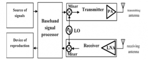
Figure 1: A basic wireless communication system
In this paper, we propose a new approach for designing a low PN oscillator presented previously in reference [8]. It is based on the Time-Invariant Linear Model (TILM) of PN [6, 8], and applied to design a MM-wave band VCO. Simulations show that the proposed architecture exhibits an extremely low phase noise level associated to a small size, compared to the ones published recently in the literature.
This paper is organized as follows. In section 2, we introduce the device technology. In section 3, a phase noise analysis is presented in order to extract an electrical model. The fourth section is dedicated to the proposed VCO architecture, while the fifth section presents the simulation results. Then we conclude.
2. GaAs pHEMT technology: PH15 UMS process
In last years, the development of III-V semiconductor materials for microwave devices has been sustained. Among these III-V semiconductors, gallium arsenide (GaAs) is the precursor, with better electronic and physical properties than silicon such as a higher electron mobility. GaAs Pseudomorphic High Electron Mobility Transistors (pHEMT) (Figure 2) are currently base of MMIC (Monolithic microwave integrated circuit) circuits thanks to mature technologies.
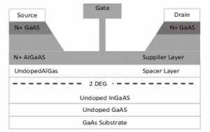
Figure 2: Cross-section of a GaAs pHEMT layers
Due to the development of these transistors, local oscillators [9], power amplifiers [10, 11], mixers [12], and frequency multipliers [13] have shown improved performances. The 5G mm-wave VCO circuit, presented in this paper, is designed using the commercial UMS foundry (PH15 process). PH15 technology is based on a classical pseudomorphic AlGaAs/InGaAs/GaAs HEMT structure shown in Figure 2. This 5G mm-wave process features typically 110 GHz-fT cut-off frequency, 640mS/mm peak transconductance, 220 mA/mm maximum drain current, -0.7 V pinch-off voltage and beyond 4.5 V gate-drain breakdown voltage. As the gate length is 0.15 µm, we take 30 µm-gate width. The PH15 process includes two metal interconnect layers, TaN resistors of 30 Ω/square, SiN MIM capacitors of 330 pF/mm2, airbridge and via holes. Table 1 shows typical datas of the pHEMT transistor [14].
Table 1: Typical data of the pHEMT Transistor
3. Voltage Controlled Oscillator Phase Noise
In wireless communication systems, a pure sine wave at a single frequency is an ideal case, i.e., a Dirac delta function at a single frequency. However, additive noise from propagation environment and circuits modulates the oscillator, introducing frequency fluctuations. These fluctuations spread the signal power at adjacent frequencies of the carrier frequency resulting in noise sidebands (Figure 3), generally named phase noise since it can be, in the time domain, represented as a random variation of the phase.
Recent wireless communication systems require radio frequency carriers of very high spectral purity. The quality of the VCO becomes a determining factor in the quality of the entire system. It would be very difficult to transmit a signal at very high frequencies and with complex modulations without a very low PN VCO.
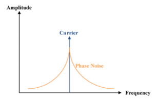
Figure 3: Phase Noise shape around the carrier frequency
The up-converted amplitude noise is a critical source to phase noise, but there are other contributors of phase noise in a LO [15], we cite for example: flicker noise, 1/f noise, thermal noise and shot noise. In order to design a LO that combines both low PN and small size, it is mandatory to find the relationship between PN and the circuit parameters. This relationship is given by the equation (1) [6]:
![]()
where is the single sideband phase noise (SSPN) at Δf offset frequency from the carrier f0, k is Boltzmann constant, T is the absolute temperature, C is the resonator capacitance value, Q is the resonator quality factor, F is noise factor and A0 is the output signal amplitude.
From equation 1, PN of the LO is reduced when increasing the quality factor of the resonator circuit, in order to improve the amplitude of the output signal [6] or increasing the value of the capacitance of the circuit. In this work, we focused on a capacitance increase. Therefore, a capacity C1 has been added, in order to enhance the capacitance value of the resonator circuit and thus improve the PN. However, as the oscillation frequency depends on the circuit capacitance, the inductance value L1 must be reduced to keep the oscillation frequency value (figure 5).
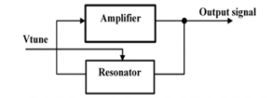
Figure 4: Synoptic diagram of a VCO
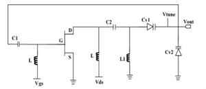
Figure 5: Colpitts VCO circuit
4. Voltage Controlled Oscillator Design
4.1. Colpitts Architecture
An oscillator (Figure 4) can be modeled by an amplifier to compensate for the energy losses, and a resonator to select the oscillation frequency [13]. The tank circuit of the Colpitts Oscillator contains a capacitive divider (two capacitors in series) and an inductance L1, while the amplifier circuit is composed of transistors with their bias elements. In [16], two varactors Cv1 and Cv2 replace fixed capacitors for purpose of tune the oscillation frequency with Vtune (figure 5). The simulation results of this VCO Colpitts show a varying oscillation frequency between 26.6 and 28.85 GHz, a PN near -96.07 and -113.07dBc/Hz@100kHz and @1MHz offset frequency respectively, and a fundamental output power of 9 dBm @ Vtune= 6 V. Although the VCO has an acceptable FoM of -172.82dBc/Hz, the PN must be improved to fulfill the 5G requirements.
4.2. Low PN VCO Architecture
In order to design a best performing VCO, an innovative architecture is proposed, studied and designed in this work. This circuit is based on the back-to-back structure of the varactors presented in [5] and on the Colpitts structure studied in [13] and [16]. Therefore, we maintained the same active part used in [13] and [16] and a capacity C1 has been added to the resonator circuit in order to enhance the capacitance value of the resonator circuit (Figure 6).
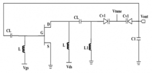
Figure 6: The proposed VCO circuit
Graphs in Figure 7 show the variation of the capacitance of the resonator versus the control voltage Vtune with and without C1. From the two graphs, we can observe that the capacitance value of the circuit is clearly increased.
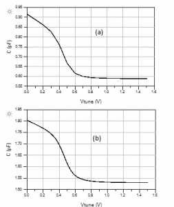
Figure 7: Capacitance value of the resonator C(V) (a) before and (b) after adding capacity C1
4.3. pHEMT VCO Layout
At mm-wave frequencies, parasitic capacitances and inductances can have a strong impact on the final Voltage Controlled Oscillator circuit performance. For this reason, a number of optimization steps were carried out before the final VCO layout presented in Figure 8.
The GaAs technology is multilayered. The chip dimensions are 0.56 x 0.423 mm2, for a surface area of 0.237 mm2. We can note that it is an extremely compact circuit compared to the architectures recently published in the literature [7, 13, 17-19].
5. Voltage Controlled Oscillator Simulation
The first step when designing an oscillator is to check the convergence of the circuit. Figure 9 shows that at 28 GHz the loop gain is 1.122 and the phase is 0.048 so both oscillation conditions in amplitude and phase are satisfied.
Simulation results on an electrical simulator software, show that the delivered signal is a sine wave (Figure 10) varying between 27.98 GHz and 29.67 GHz (Figure 11). Therefore, the tuning range (TR) is 1.69 GHz (about 6% of central frequency).
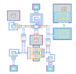
Figure 8: Layout of the proposed 5G mm-wave Voltage Controlled Oscillator
At the frequency 28.97 GHz (Vtune = 2.00 V), phase noise equals to -113.073, -133.078 and -153.07 dBc/Hz @ 100kHz, 1MHz and 10MHz offset frequency respectively (Figure 12). We can deduce that is an ultra-low PN level. Nevertheless, this architecture has an ultra-low PN only in a small tuning range part (around 28.95 GHz) (Figure 13), outside, the PN level is increased by 15 dB, i.e. the PN increases until it reaches the value -133.3 dBc/Hz @10MHz offset. Anyway, the PN of this architecture remains low compared to the other architectures recently published.
The fundamental output power is 3.26 dBm, on the other hand, at the first and second harmonics, it is equals to -18.8 dBm -14.2 dBm, respectively. Thus, the first and second harmonic rejections are 22.05 dB and 17.45 dB respectively (Figure 14). The DC power consumption is about 51 mW.
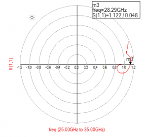
Figure 9: Loop gain of the VCO
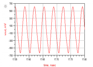
Figure 10: Time domain of Vout for Vtune=2 V
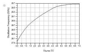
Figure 11: Variation of the oscillation frequency versus Vtune
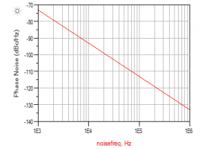
Figure 12: Single Sideband Phase Noise for Vtune=2 V
6. Analysis of the simulation results
Table 2 presents the performance of the designed LO architecture compared to other architectures recently published in the literature. The PN of our architecture is 21.2 dB lower than the architecture proposed in [17] and beyond 22.5 dB, 22.1 dB and 14 dB lower than the architecture designed in [7], [13] and [18] respectively. Our VCO also has a relatively a wide tuning frequency range of about 1.67 GHz and a high fundamental output power of 3.26 dBm. The circuit consumption is quite low, less than half the DC power consumed by the VCO circuits studied in [7] and [19]. Finally, our LO has a good FoM of -195.3 dBc/Hz and is very small chip size compared to other architectures [7, 17-19].
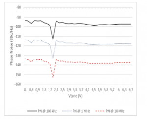
Figure 13: Single Sideband Phase Noise versus Vtune
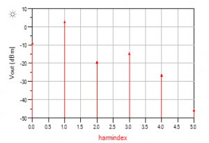
Figure 14: Spectral output power Vout for Vtune=2V
Table 2: Performance of different VCOs recently published in the literature
| Ref. | Oscillation frequency (GHz) | DC power consumption (mW) | Fundamental output power (dBm) | PN (dBc/Hz) @1MHz | FoM** (dBc/Hz) | Chip area (mm2) | Technologie |
| [17] | 28.3 | – | 11.8 | -102 | – | 0.5 | 0.15 µm pHEMT |
| [7] | 29.4 | 124.6 | 4.5 | -100.7 | -169.11 | 3.75 | 0.13 µm SiGeBiCMOS |
| [13] | 28.02 | 96 | 5 | -100.9 | -180.37 | 0.25 | 0.15 µm GaAs pHEMT |
| [19] | 27.7 | 122 | 9.75 | -113.16 | -181.06 | 0.515 | 0.15 µm GaAs pHEMT |
| [18] | 28.1 | 20 | – | -109.2 | -184.2 | 0.24 | 22 nm CMOS |
| This work | 28.8 | 51 | 3.26 | -123.2* | -195.3 | 0.237 | 0.15 µm GaAs pHEMT |
(*) The average value of PN
Where is the PN @ offset from the and is the DC power consumption of the circuit in mW.
7. Conclusion
A new design approach for a low PN VCO is proposed, studied, and validated in this paper. This approach has enabled the design of a LO for the 5G mm-Wave band of low PN of -123.2 dBc/Hz @1MHz offset frequency from carrier, with a TR of 1.69 GHz, a fundamental output power of about 3.26 dBm associated to low DC power consumption.
- B. Dzogovic, B. Santos, T. Van Do, B. Feng, T. Van Do, and N. Jacot, “Bringing 5G Into User’s Smart Home” in 2019 IEEE Intl Conf on Dependable, Autonomic and Secure Computing, Intl Conf on Pervasive Intelligence and Computing, Intl Conf on Cloud and Big Data Computing, Intl Conf on Cyber Science and Technology Congress, Fukuoka, Japan, 2019.https://doi.org/10.1109/DASC/PiCom/CBDCom/CyberSciTech.2019.00145.
- D. Milovanovic and Z. Bojkovic, “5G Mobile Networks: What is Next?” International Journal of Communications, 4, 1-5, 2019.
- G. Kang, S. Jiang, and Z. Zhao, “Research on millimeter wave spectrum planning for 5G” J. Phys. Conf. Ser., 1345, 1-5, 2019. https://doi.org/10.1088/1742-6596/1345/3/032040.
- International Telecommunication Union, “Key outcomes of the World Radiocommunication Conference 2019” ITU News Magazine, 6, 1-56, 2019.
- J. Hyvert, D. Cordeau, and J.-M. Paillot, “Analysis and design of a very low phase-noise Ku-band coupled VCO using a modified cascode architecture in 0.25 μm SiGe:C BiCMOS technology” Microelectron. J., 75, 137–146, 2018. https://doi.org/10.1016/j.mejo.2018.04.002.
- L. Romanò, V. Minerva, C. Samori, and M. Pagani, “Low Phase Noise, Very Wide Band SiGe Fully Integrated VCO” in 12th Gallium Arsenide applications symposium, Amsterdam, 2004.
- G. Cheng, Z. Li, Z. Li, T. Han, and M. Tian, “A 22-to-36.8 GHz low phase noise Colpitts VCO array in 0.13-μm SiGe BiCMOS technology” Microelectron. J., 88, 79–87, 2019. https://doi.org/10.1016/j.mejo.2019.04.004.
- A. Es-Saqy, M. Abata, S. Mazer, M. Fattah, M. Mehdi, M. El Bekkali, C. Algani, “Very Low Phase Noise Voltage Controlled Oscillator for 5G mm-wave Communication Systems” in 2020 1st International Conference on Innovative Research in Applied Science, Engineering and Technology (IRASET), Meknes, Morocco, 2020. https://doi.org/10.1109/IRASET48871.2020.9092005
- A. Es-saqy, M. Abata, M. Fattah, S. Mazer, M. Mehdi, M. El bekkali, “Study and Design of a MMIC Voltage Controlled Oscillator for 5G mm-wave band Applications” Int. J. Adv. Trends Comput. Sci. Eng., 9(2), 2124–2129, 2020. https://doi.org/10.30534/ijatcse/2020/186922020.
- H. Lee, W. Lee, T. Kim, M. Helaoui, F. M. Ghannouchi, and Y. Yang, “6–18 GHz GaAs pHEMT Broadband Power Amplifier Based on Dual-Frequency Selective Impedance Matching Technique” IEEE Access, 7, 66275–66280, 2019. https://doi.org/10.1109/ACCESS.2019.2917699.
- Y. Chen, C.-N. Chen, C.-C. Chiong, and H. Wang, “A Compact 40-GHz Doherty Power Amplifier With 21% PAE at 6-dB Power Back Off in 0.1um GaAs pHEMT Process” IEEE Microw. Wirel. Compon. Lett., 29(8), 545–547, 2019. https://doi.org/10.1109/LMWC.2019.2925716.
- C. Wang, D. Hou, J. Chen, and W. Hong, “A Dual-Band Switchable MMIC Star Mixer” IEEE Microw. Wirel. Compon. Lett., 29(11), 737–740, 2019. https://doi.org/10.1109/LMWC.2019.2940637.
- M. Kim, K. Choi, and J. Kim, “W-Band Backward Distributed Frequency Doubler Using GaAs 0.15 um pHEMT Process,” IEEE Microw. Wirel. Compon. Lett., 29(6), 400–402, 2019. https://doi.org/10.1109/LMWC.2019.2913307.
- PH15-UMS MMIC Foundry, 2015-2016 Foundry Brochures.
- A. Hajimiri, “A General Theory of Phase Noise in Electrical Oscillators” IEEE JOURNAL OF SOLID-STATE CIRCUITS, 33(2), 179-194, 1998.
- A. Es-Saqy, M. Abata, S. Mazer, I. Halkhams, M. Mehdi, and C. Algani, “Comparative Study Between Hartley and Colpitts VCO for 5G MM-Wave Band Applications” in 2019 7th Mediterranean Congress of Telecommunications (CMT), Fès, Morocco, 2019. https://doi.org/10.1109/CMT.2019.8931343.
- B. Piernas, K. Nishikawa, T. Nakagawa, and K. Araki, “A compact and low-phase-noise Ka-band pHEMT-based VCO” IEEE Trans. Microw. Theory Tech., 51(3), 778–783, 2003. https://doi.org/10.1109/TMTT.2003.808584.
- M. A. Shehata, M. Keaveney, and R. B. Staszewski, “A 184.6-dBc/Hz FoM 100-kHz Flicker Phase Noise Corner 30-GHz Rotary Traveling-Wave Oscillator Using Distributed Stubs in 22-nm FD-SOI” IEEE Solid-State Circuits Lett., 2(9), 103–106, 2019. https://doi.org/10.1109/LSSC.2019.2929326.
- A. Es-Saqy, M. Abata, M. Mehdi, S. Mazer, M. Fattah, M. El bekkali, C. Algani, “28 GHz Balanced pHEMT VCO with Low Phase Noise and High Output Power Performance for 5G mm-Wave Systems” Int. J. Electr. Comput. Eng., 10(5), 2020. http://doi.org/10.11591/ijece.v10i5.pp%25p.
No related articles were found.