Experimental Studies of the Silicon Photomultiplier Readout Electronics Based on the Array Chip МН2ХА030

Adv. Sci. Technol. Eng. Syst. J. 5(3), 108–114 (2020);
 DOI: 10.25046/aj050314
The experimental findings of the main units of readout electronics of silicon photomultipliers (SiPMs) based on array chip (AC) МН2ХА030: a charge-sensitive amplifier (CSA) with an adjustable conversion factor and a base line restorer (BLR) circuit and two types of voltage comparators are considered. The electrical circuits of the units, the measurement results of static and dynamic parameters are given.
1. Introduction
Silicon photomultipliers are successfully used in a number of fields of science and technology for recording various types of electromagnetic radiation [1-10], because they have smaller dimensions, supply voltage and noise [11-13] in comparison with vacuum PM tubes. To process SiPM signals are usually used specialized analog integrated circuits (ICs), optimized according to the parameters of the signal source – internal capacitance, amplitude and duration of the current pulse.
SiPM readout electronics are relatively not required and their development costs too much. This explains the importance of creating specialized ICs on the ACs. So, we developed the main units of SiPM readout electronics at AC МН2ХА030:
- the CSA with an adjustable conversion factor and a BLR circuit called ADPreampl3 [11];
- analog interface with a large dynamic range IBUF [14];
- different types of voltage comparators [15].
The purpose of this article is to consider the experimental findings of amplifier ADPreampl3 and comparators ADComp1, ADComp3 made on AC МН2ХА030.
2. Circuitry Features of the Analog Units under Study
A detailed description of the operation of amplifier ADPreampl3 and comparators ADComp1, ADComp3 is given in [11,15]. When they were implemented at the AC, minimal corrections were made, caused by a slight change in the resistances of the resistors and the formation of diodes at the p-n junctions of the field effect transistor.
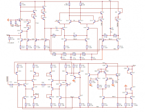
Figure 1: The electrical circuit of amplifier ADPreampl3
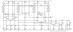
Figure 2: The electrical circuit of comparator ADComp1
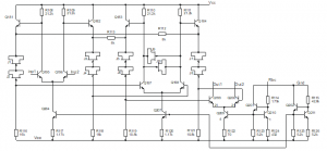
Figure 3: The electrical circuit of comparatorADComp3
Electrical circuits of ADPreampl3, ADComp1, ADComp3 are shown in Figures 1-3. Note that all nodes with the same name, for example, VСС, VEE, G-, G+, Bias1, Bias2, Fil in Figure 1 are interconnected, and, if necessary, the scaling factors are given in the diagrams, showing the number of the AC transistors connected in parallel. So, the emitter junction area of transistor Q19 in Figure 1 corresponds to the area of the emitter junctions of the 21st parallel-connected n-p-n-transistor of the AC.
The values of the resistances R7 = 184 Ohms,
R74 = 375 Ohms, R124 = 432 Ohms are shown in Figure 1, Figure 2 and Figure 3 with great accuracy, but these are not necessary conditions. In the circuit, these resistor values are obtained with parallel and serial connection of the 1.05 kOhms and 2.45 kOhms resistors available on the AC.
It is worth noting that there is no need for special use of the p-JFET. These transistors are formed on the AC and are used only in diode connections.
Assignment of the nodes in the circuits of Figures 1-3 are the following.
For ADPreampl3: VСС, VEE – positive and negative supply voltage; InpA – amplifier input; FOut – output of the fast signal circuit (SC), OutA, OutAinv – direct and inverse output of the slow SC, FOutShift – voltage that sets the base line (dc output voltage in the absence of an input signal) by the output of the fast SC, OutAShift – voltage that sets the base line by the outputs of the slow SC, Gain – voltage that sets the value of the charge-voltage conversion factor KQV by the outputs of the slow SC, Bias – node for connecting a current source that sets the operation mode of the amplifier.
For ADComp1, ADComp3: VСС, VEE – positive and negative supply voltage; Gnd – bus of null potential (“ground”); Inp1, Inp2 – inputs; Out1, Out2 – outputs; Rbc – node for connecting a voltage source that sets the maximum output current of the comparator, usually this node is connected to null potential.
Comparator ADComp3 is a simplified version of ADComp1 and is designed to reduce the AC area occupied by the comparator circuit. So, in total 8 units of ADComp1 or 16 units of ADComp3 can be manufactured at AC МН2ХА030. On the manufactured experimental samples, comparator ADComp3 was made in two-channel design.
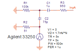
Figure 4: The simplified electric equivalent circuit of SiPM Photonique with 516 microcells, used in measurements
3. Measurement Results
Experimental samples of AC МН2ХА030 with analog units were manufactured at JSC “Integral” (http://www.integral.by/). Measurements were performed using a set of equipment, including signal generators Agilent 33250 and Tektronix AFG3152C, a set of fixed attenuators, digital oscilloscope GDS 73354, dual-channel voltage supply source Agilent 3646A, data acquisition system 34970A with a set of modules, and digital multimeter Agilent 34410A. The signal came at the input of ADPreampl3 from the electric equivalent circuit SiPM Photonique with 516 microcells [11] (Figure 4), where TR, TF, PW, PER, V1, V2 are parameters of the rectangular voltage source used, namely, the rise and fall times, pulse duration, period, initial and final voltage values, correspondingly. By setting different voltages of V2, it is possible to continuously change the input charge of the amplifier in accordance with the relation QINP=C2·V2, or when the voltage of V2 is a multiple of 1.7 mV, which corresponds to one switched on cell, set the value of input charge N of the switched-on microcells of SiPM Photonique. The pulse duration of the generator is chosen equal to 500 ns in order to register the output pulses of ADPreampl3 of different polarity after the output signal reaches the base line.
In the comparator measurements, the same common-mode signal VCM came simultaneously to both inputs, and a rectangular voltage pulse symmetrical with respect to the common-mode signal with a rise and fall front duration of 3 ns and a peak-to-peak value equal to VINP was additionally received at one of the inputs. Both outputs of the comparators were connected through resistors with a resistance of 50.5 Ohms to the bus of null potential.
In total 20 units of amplifiers ADPreampl3, 10 units of dual-channel comparators ADComp3 and single-channel comparators ADComp1 were measured. Figures 5-14 and the table show the main measurement results, and the figures show the dependencies closest to the average.
Measurements made it possible to establish the following.
1) The spread of the base line by output FOut ranged from minus 24 mV to 276 mV with an average value of 85.6 mV. In this case, a voltage change in the node FOutShift from -3 V to 3 V is sufficient to establish a base line value of FOut output close to zero.
2) When the BLR circuit was switched off (the node OutAShift was not connected to any voltage), the spread of the base line at the output OutA was from 300 mV to 800 mV. When connecting the node OutAShift to the bus of null potential, the average base line value for the output OutA was 3.72 mV, and for the output OutAinv it was minus 2.42 mV.
3) The BLR circuit enables to smoothly change the base line at the outputs OutA, OutAinv in the range of ± 0.9 V.
4) When developing analog units, it was assumed that the output signal of amplifier ADPreampl3 would come to the input of the comparator with a small input capacitance. In connection with the above, the output stages of the amplifier are simple emitter followers on n-p-n-transistors and the voltage pulse shape at the outputs FOut, OutA, OutAinv depends on the input capacitance of the oscilloscope, which leads to different output pulses in the positive and negative half-waves. If necessary, the influence of the load capacitance on the shape of the output pulse can be reduced by using an emitter follower on complementary bipolar transistors, as in operational amplifiers previously developed on AC МН2ХА030 [16]. Such an output stage increases the current consumption of the amplifier and therefore its use is carried out only in justified cases. To exclude the influence of the capacitance of the oscilloscope on the shape of the output pulses, a non-inverting voltage follower on chip AD8132 connected to the pins FOut, OutA, OutAinv was used in the measurements.
As can be seen from Figure 5, Figure 6, the inclusion of the follower provides almost the same shapes of the output pulses of both polarities.
5) At the maximum gain required to register the signal of 2 microcells of SiPM Photonique switched-on, the dynamic range of ADPreampl3 exceeds 20 dB, however, in this case, the conversion factor KQV depends on the input charge QINP (Figure 7, 8).
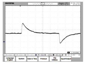
Figure 5: The voltage pulses at the output FOut for 10 switched-on microcells of SiPM Photonique when the voltage follower is used
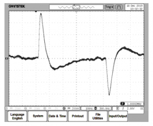
Figure 6: The voltage pulses at the output OutA for 10 switched-on microcells of SiPM Photonique when the voltage follower and the BLR circuit is used
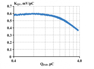
Figure 7: The dependence of the maximum value of the conversion factor KQV at the output OutA on the value of the input charge QINP
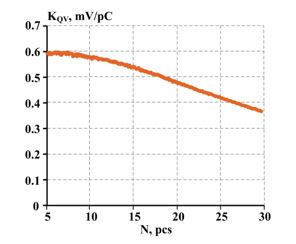
Figure 8: The dependence of the maximum value of the conversion factor KQV at the pin OutA on the value of N switched-on microcells of SiPM Photonique
In the case when it is necessary to register the input charge from more than 30 switched-on microcells of SiPM Photonique, it is recommended to reduce the output pulse by reducing the voltage at the Gain pin (Figure 9) or use the signal from the pin FOut (Figure 10). To significantly increase the dynamic range, it is advisable to use new circuitry solutions, for example, considered in [14].
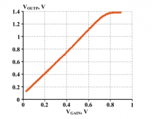
Figure 9: The dependence of the value of the pulse at the output OutA (VOUTP) on the voltage at the pin of the Gain (VGAIN)
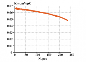
Figure 10: The dependence of the conversion factor KQV at the pin FOut on the value of N of switched-on microcells of SiPM Photonique
6) As follows from the table, the measured values of the static parameters of the comparators are close to the simulation results.
Table 1: Measurement and Simulation Results of the Basic Parameters of Comparators at the Supply Voltage Value, Equal to ± 3.0 V
| Parameter Name | Parameter value | |||
| ADComp1 | ADComp3 | |||
| measurements | simulation | measurements | simulation | |
| Input current IINP, μA | 0.7-0.8 | 0.58 | 0.5-0.7 | 0.5 |
| Maximum output current IOUT, mA | 3.2-3.4 | 4.03 | 2.8-3.0 | 4.0 |
| Sensitivity, mV | 2.0 | 2.0 | 2.0 | 2.0 |
The output current of the comparators is less according to the measurement results than in the simulation, as shown in Table 1. The dynamic parameters of the comparators characterize the dependencies shown in Figure 11 – Figure 14. It is possible to connect the Rbc node to an external voltage source by adjusting the output current. However, this requires an additional highly stable voltage source. We plan to reduce the resistance of the current-setting resistors with the closest adjustment of the interconnections of the elements of the AC. In this case, the output current of the comparators will increase even when the Rbc node is connected to zero voltage.
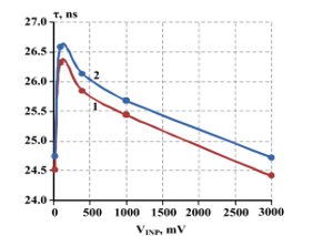
Figure 11: The dependence of the average signal propagation delay in two-channel comparator ADComp3 on the amplitude of the input signal for the first (1) and second (2) channels
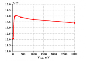
Figure 12: The dependence of the average signal propagation delay in comparator ADComp1 on the amplitude of the input signal 7) The measurements revealed a lower value of the maximum output current of the comparators and a significant excess of the measured values of the peak time of ADPreampl3 and the signal propagation delay of the comparators over the values obtained during the simulation.
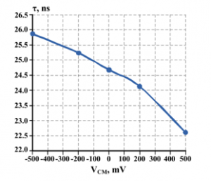
Figure 13: The dependence of the average signal propagation delay in two-channel comparator ADComp3 on the value of the common-mode signal at VINP = 20 mV
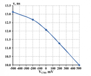
Figure 14: The dependence of the average signal propagation delay in comparator ADComp1 on the value of the common mode signal at VINP = 20 mV
From our point of view, the insufficient value of the maximum output current of the comparators is due to the difference in the current-setting resistors of the output stages (R72 in Figure 2, R122 in Figure 3) from the required value and can be eliminated when adjusting the interconnects of the AC elements.
The Spice parameters CJE, CJC, CJS of the AC МН2ХА030 transistors used in the simulation were obtained from the identified parameters for transistors with a large layout area by decreasing in proportion to the area of the emitter junction. For the transistors of AC МН2ХА030 made according to the minimum design rules, such scaling of the Spice parameters turned out to be incorrect and identification of the Spice parameters CJE, CJC, CJS by the results of measurements of experimental samples is required.
4. Conclusion
It was experimentally established that the created base line restorer circuit reduces the spread of the base line of amplifier ADPreampl3 by almost 100 times and enables to smoothly change the base line at the outputs OutA, OutAinv in the range of ± 0.9 V.
At maximum gain, the dynamic range of ADPreampl3 exceeds 20 dB, however, in this case, the conversion factor depends on the value of the input charge. To register large input charges, it is recommended to reduce the output pulse by reducing the voltage at the Gain pin or process the signal from the pin FOut.
The static and dynamic parameters of created comparators ADComp1, ADComp3 satisfy the requirements for readout electronics of silicon photomultipliers.
The measurements revealed a mismatch between the results of simulation and measurements of the maximum output current of the comparators, the peak time of the amplifier and the signal propagation delays of the comparators, therefore, in the near future, it is planned to adjust the interconnects of the AC elements to increase the maximum output current and refine the Spice parameters of transistors according to the measurement results of experimental samples.
The developed units can be used to create multichannel signal processing circuits of SiPM based on AC МН2ХА030.
Conflict of Interest
The authors declare that there is no conflict of interests regarding publication of this paper.
Acknowledgment
The study has been carried out at the expense of the grant from the Russian Science Foundation (Project No.16-19-00122-P).
- G. Paternoster, L. Ferrario, F. Acerbi, A. G. Gola and P. Bellutti, “Silicon Photomultipliers Technology at Fondazione Bruno Kessler and 3D Integration Perspectives,” ESSDERC 2019 – 49th European Solid-State Device Research Conference (ESSDERC), Cracow, Poland, 2019, pp. 50-53. DOI: 10.1109/ESSDERC.2019.8901738
- W. Jiang, Y. Chalich, M. J. Deen, “Sensors for Positron Emission Tomography Applications,” J. Sensors 2019, 19, 5019; DOI: 10.3390/s19225019.
- R.R. Raylman, A. Stolin, S. Majewski, and J. Proffitt, “A large area, silicon photomultiplier-based PET detector module,” Nucl. Instrum. and Methods A, vol. 735, pp. 602-609, 2014. DOI: 10.1016/j.nima.2013.10.008
- A.L. Goertzen, et al., “Design and performance of a resistor multiplexing readout circuit for a SiPM detector,” IEEE Trans. Nucl. Sci., vol. 60, no 3, part 1, pp. 1541-1549, 2013. DOI: 10.1109/TNS.2013.2251661
- S. Dey, E. Myers, T.K. Lewellen, R.S. Miyaoka, and J.C. Rudell, “A row-column summing readout architecture for SiPM based PET imaging systems,” IEEE Nucl. Sci. Symp. and Med. Imag. Conf. (NSS/MIC),
pp. 1-5, Oct. 27 2013-Nov. 2 2013. DOI: 10.1109/NSSMIC.2013.6829062 - S. Gundacker, et al., “A systematic study to optimize SiPM photodetectors for highest time resolution in PET,” IEEE Trans. on Nucl. Sci., vol. 59, no 5, part 1, pp. 1798-1804, 2012. DOI: 10.1109/TNS.2012.2202918
- A. Del Guerra, et al., “Silicon Photomultipliers (SiPM) as novel photodetectors for PET,” Nucl. Instrum. and Methods A, vol. 648, pp. S232 – S235, 2011. DOI: 10.1016/j.nima.2010.11.128
- Xiaoli Li, C. Lockhart, T.K. Lewellen, and R.S. Miyaoka, “Study of PET detector performance with varying SiPM parameters and readout schemes,” IEEE Trans. on Nucl. Sci., vol. 58, no 3, part 1, pp. 590-596, 2011. DOI: 10.1109/TNS.2011.2119378
- B. Seitz, A. G. Stewart, K. O’Neill, L. Wall, and C. Jackson, “Performance Evaluation of Novel SiPM for Medical Imaging Applications,” J. Photonics, 2014, no. 1 (43), Pp.104-113. DOI: 10.1109/NSSMIC.2013.6829685
- H. Sabet, et al., “High-performance and cost-effective detector using microcolumnar CsI:Tl and SiPM,” IEEE Trans. on Nucl. Sci., vol. 59, no 5, part 1. pp. 1841-1849, 2012. DOI: 10.1109/TNS.2012.2202248
- O.V. Dvornikov, V. A. Tchekhovski, N. N. Prokopenko, Ya. D. Galkin, A. V. Kunts, A. V. Bugakova, “Implementation of Reading Electronics of Silicone Photomultiplier Tubes on the Array Chip MH2XA030,” Visnyk NTUUKPI Seriia–Radiotekhnika Radioapara to buduvannia, 2019, Iss.78, pp.60–66. DOI: 10.20535/RADAP.2019.78.60-66.
- O. V. Dvornikov, V. A. Tchekhovski, V. L. Diatlov, “Equipments to single photon registration. Part 1. Features and possibilities of multi-channel photodetectors with intrinsic amplification,” Devices and methods of measurements : Scientific and Engineering J., 2012, no. 2(5), Pp. 5–13. (In Russian)
- O. V. Dvornikov, V. A. Tchekhovski, V. L. Diatlov, “Equipments to single photon registration. Part 2. Silicon photomultiplier signal preliminary processing. (Review) ,” Devices and methods of measurements : Scientific and Engineering J., 2013, no. 1 (6), Pp. 5–13. (In Russian)
- O. V. Dvornikov, N. N. Prokopenko, V. A. Tchekhovski, Y. D. Galkin, A. E. Titov and A. V. Bugakova, “Silicon Photomultipliers’ Analog Interface with Wide Dynamic Range,” Proceedings of 17th IEEE East-West Design & Test Symposium (EWDTS-2019), September 13-16, 2019, Batumi, Georgia, pp. 270-273. DOI: 10.1109/EWDTS.2019.8884430.
- O.V. Dvornikov, N. N. Prokopenko, V. A. Tchekhovski , Ya. D. Galkin, A. V. Kunz, A. Titov, “Radiation-Hardened Voltage Comparators for the Synthesis of Microcircuits on the Array Chip MH2XA030,” Proceedings of IEEE International Conference on Computation, Automation and Knowledge Management (ICCAKM – 2020), 9-11 January 2020, Dubai, Pp. 1-4.
- O. V. Dvornikov, V. L. Dziatlau, V. A. Tchekhovski, N. N. Prokopenko and A. V. Bugakova, “BiJFet Array Chip MH2XA030 — a Design Tool for Radiation-Hardened and Cryogenic Analog Integrated Circuits,” 2018 IEEE International Conference on Electrical Engineering and Photonics (EExPolytech), St. Petersburg, 2018, pp. 13-17. DOI: 10.1109/EExPolytech.2018.8564415