
Comparison of the RC-Triggered MOSFET-Based ESD Clamp Circuits for an Ultra-low Power Sensor System
Volume 5, Issue 2, Page No 718-723, 2020
Author’s Name: Chih-Hsuan Lina), Kuei-Ann Wen
View Affiliations
Department of Electronic Engineering, University of National Chiao Tung (NCTU), Hsinchu 300, Taiwan
a)Author to whom correspondence should be addressed. E-mail: shsuanhsuan.ee01g@g2.nctu.edu.tw
Adv. Sci. Technol. Eng. Syst. J. 5(2), 718-723 (2020); ![]() DOI: 10.25046/aj050289
DOI: 10.25046/aj050289
Keywords: ultra-low power, ESD, accelerometer

Export Citations
This paper uses the RC-triggered MOSFET-based electrostatic discharge (ESD) power clamp to conduct ESD from ESD events and not affect the ultra-low power sensor system. Then using the stacked device include stacked MOSFET or stacked BJT to reduce the leakage current which increases with temperature. Moreover, we compare gate-driven method and two-level–driven with both gate-driven and substrate-driven methods to determine the most efficient method in terms of layout area, leakage current, Human Body Model (HBM)/Machine Model (MM), and turn-on time. The proposed design of the power ESD clamp (IO15c/IO15e/IO15c_resize) has an HBM ESD protection level with a Positive higher than 8KV, 5.5KV, 8KV, and an MM ESD protection level with a Positive higher than 600V, 300V, 1000V. The power ESD clamp (IO15c/IO15e) consumes nearly 3.5pW/16.45nW and 2.8pW/16.89nW at temperatures of 25°C and 125°C, respectively, when AVDD3 is 1.0V.
Received: 17 February 2020, Accepted: 11 April 2020, Published Online: 20 April 2020
1. Introduction
With internet of things applications being used in handheld devices, mobile phone standby time is becoming a key focus of consumers’ attention. It has become increasingly important to study ultra-low power sensing systems in order to increase standby time. Nowadays, such systems generally reduce power consumption to less than the microwatt level. However, the current of traditional electrostatic discharge (ESD) power clamp leakage currents at high temperatures is greater than 1uA for a 180nm complementary metal-oxide-semiconductor (CMOS) process. This leakage current affects the stability of the ultra-low power sensor system. This paper uses the RC-triggered metal–oxide–semiconductor field-effect transistor (MOSFET)-based ESD power clamp to conduct ESD from ESD events and not affect the ultra-low power sensor system. Then, a stacked device, including a stacked MOSFET or stacked BJT, is used to reduce the leakage current that increases with temperature. However, the disadvantage of using a stacked device is that its size will be proportional to the number of stacked layers. This is because the stacked device must keep a certain ON-resistance as the BIGFET of the ESD power clamp (IO1) to keep the rate of heat flow and maintain the ESD level. Moreover, this paper compares two methods to determine which method is the most efficient in terms of layout area, leakage, Human Body Model (HBM)/Machine Model (MM), and turn-on time. The methods are the gate-driven method and two-level–driven method with both the gate-driven and substrate-driven methods.
In addition, some microelectromechanical systems (MEMS) with small gap spacing operate using electrostatic forces. This may cause damage to their structures due to surface roughness, variations in structure geometries, variable gap spacing, and flexible moving components [1]. Further analysis of the problem determines that ESD is an effective charge injection source, which is considered to be a major reliability issue in MEMS [2]. In some studies, an analytical method of charge injection is performed, including using ESD in MEMS [3], [4]. This paper presents whole-chip ESD protection with an ultra-low power ESD clamp circuit to be applied to a 3D accelerometer.
In this paper, the proposed ESD power clamp can be fabricated using the Uniform Mechanical Code (UMC) 0.18mm standard CMOS-MEMS process. This paper is organized as follows: Section 1. introduces the ESD power clamp; Section 2. describes the ESD power clamp architecture considerations; Section 3. compares the RC-triggered MOSFET-based ESD clamp circuits and design; and Section 4. describes the measurement results and discussion.
2. Architecture considerations
Figure. 1 shows a schematic view of a sensor and the architecture of a whole-chip ESD protection circuit. The functions are detailed as follows: 1) When the input pin (VM) is zapped, the ESD current is led away by A_PATH from the VM node through Q2, Q1 to VSUB; 2) When the input pin (VM) is zapped, the ESD current is led away by B_PATH from the VM node through Q2, Q1, D1, D2, Q5 to VDN; 3) When the input pin (AVDD) is zapped, the ESD current is led away by C_PATH from the AVDD node through Q1 to VSUB; 4) When the input pin (VDN) is zapped, the ESD current is led away by D_PATH from the VDN node through Q5, D4, D3, Q1 to AVDD; 5) When the input pin (VUP) is zapped, the ESD current is led away by E_PATH from the VUP node through Q1 to VSUB. 6) The zone with the black dotted line portrays the sensor model, and the accelerometer sensor is modeled by C1, C2, C3, C4, and C5 [5], [6]. When different ESD events occur, the electrostatic current will be led away through different paths, including A_PATH, B_PATH, C_PATH, D_PATH, E_PATH, and ESD power clamp (Q1). The electrostatic current does not affect the performance of the sensor system and all of the junctions of the device are forward-biased for different paths. The forward-biased junction of the device generates less the rate of heat flow than the reverse-biased junction of the device and can improve ESD protection capability.
 Figure. 1. Sensor and ESD protection circuit
3. Comparison the RC-triggered MOSFET-based ESD clamp circuits and designs
3.1. The RC-triggered MOSFET-based power clamp [7]
From the sensor and ESD protection circuit shown in Figure. 1, the ESD power clamp (Q1) is a large dimension of a 3.3V device to keep a certain ON-resistance and the rate of heat flow. The ESD power clamp (Q1) acts as the voltage gate in a low setting and will be divided into several 3.3V devices in parallel due to process reliability. The disadvantage of the ESD power clamp (Q1) is that it has a non-uniform conduction issue. When an ESD event occurs, the ESD power clamp (Q1) will be turned on, but the ESD power clamp (Q1) cannot simultaneously perform uniform conduction and degrade ESD protection capabilities. To solve the non-uniform conduction issue, an ESD power pad (IO1) is often used. The ESD power pad (IO1) is an RC-filter and inverter that forms a RC-transient detector to detect an ESD event, as shown in the blue box in Figure. 2. When an ESD event occurs, the device (M2) is turned on and the detection point (O1) is pulled to a high setting. Then, the BIGFET is turned on and the electrostatic current travelling through the BIGFET is lead away. When the ESD event disappears, the device (M2) returns to a normal state, the detection point (OI) is pulled to a low setting, and the BIGFET stops conducting. Moreover, the ESD protection circuit uses a 3.3V device and a UMC ESD standard process, including a thinner gate oxide, shorter channel length, shallower drain/source junction, silicide block (SAB), Local Oxidation of Silicon/shallow trench isolation, lightly-doped drain/ESD-implantation structure, and layout rule. The layout rule includes SAB width, SAB to poly gate edge spacing, an n-type metal–oxide–semiconductor (NMOS) layout with inner N-well ring, channel width, channel length, drain contact to poly gate, source contact to poly gate, spacing from drain diffusion to guarding diffusion, etc. The overall power consumption of the ultra-low power sensor system is, however, at the microwatt level. When the ESD event disappears, the BIGFET is turned off and the BIGFETs leakage current will increase as the temperature rises. It will affect the overall performance of the ultra-low power sensor system. To solve this issue, the RC-triggered MOSFET-based power clamp (IO15) is used. [7]
 Figure. 2. ESD power clamp (IO1)
The IO15 description is as follows: The RC-transient detector, which is the RC-filter and inverter is the same as the ESD power clamp (IO1), and the ESD power clamp (IO15) uses a delay-line to divide into two paths, as shown by the red line in Figure. 3. The delay-line with parasitic capacitor (CL) increases the fully-on time of a stacked device (MN6_1 and MN6_2), which is separated from the BIGFET of the ESD power clamp (IO1) for the ESD event. Then, the ESD power clamp (IO15) uses the output of the delay-line to control the gate voltage of the stacked device. Moreover, it uses the stacked device to reduce the leakage current, and uses the RC-transient detector to control the delay-cell of small dimension size to lower the detection point (O1) time, as shown in Figure. 3. The capacitor uses a metal-oxide-metal capacitor to reduce the leakage current. The device sizes of the ESD power clamp (IO15) are chosen as Table 1.
Table 1. The device sizes of the ESD power clamp (IO15)
| Name | W/L | Name | W/L | ||
| MP1 | 6um/0.4um | MN1 | 1.5um/0.4um | R | 50.33K |
| MP2_1 | 6um/0.4um | MN2_1 | 3.0um/0.4um | C | 2.5P |
| MP3_1 | 6um/0.4um | MN3_1 | 3.0um/0.4um | ||
| MP4_1 | 21um/0.4um | MN4_1 | 8.0um/0.4um | ||
| MP5_1 | 21um/0.4um | MN5_1 | 8.0um/0.4um | ||
| MP6_1N | 864um/0.38um | MP6_2N | 864um/0.38um |
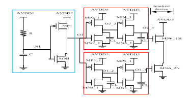 Figure. 3. ESD power pad circuit (IO15) 3.2. Comparison of the RC-triggered MOSFET-based power clamp with the gate-driven method and two-level–driven with both the gate-driven and substrate-driven methods
Because the stacked device must keep a certain ON-resistance and the rate of heat flow as the BIGFET of the ESD power clamp (IO1) and maintain the ability ESD, the size of the stacked device will be proportional to the number of stacked layers. Then gate-driven method and two-level–driven with both gate-driven and substrate-driven methods are compared, respectively, to determine which method is the most efficient in terms of layout area, leakage, HBM/MM, and turn-on time. The gate-driven method, two-level–driven with both gate-driven and substrate-driven methods describe as follows.The ESD power clamp (IO15c) uses RC-transient detector detect and delay-line as the IO15 and controls the gate voltage of the stacked MOSFET. The ESD power clamp (IO15c) uses the gate-driven method and the cross section of a stacked MOSFET, as shown in Figure. 4. When an ESD event occurs, the RC-transient detector pulls O1 to a high setting, then, through the delay-line, divides into two paths and controls the stacked MOSFET. The path from the top side controls the gate voltage (G1) of MNO1_1~MNO1_28 and the path from the bottom side controls the gate voltage (G2) of MNO2_1~MNO2_28. The electrostatic current will be divided into 28 paths, and heat will be generated from AVDD3 to GND, via the stacked MOSFET (MNO1_1 and MNO2_1) ~ (MNO1_28 and MNO2_28). The heat can be evenly distributed to different junctions to avoid thermal runaway. When the ESD event disappears, the stacked MOSFET is turned off and the leakage current is lower than the ESD power clamp (IO1). By using the gate-driven method, the positive gate voltage will form strong versions of NMOS channels and will cause electrostatic currents to flow through junctions, which are very shallow in depth. This will degrade ESD capability. The substrate-driven method can be used to avoid this issue [8] by having lower ON-resistance characteristics and evenly dissipating heat to a deeper junction to increase ESD capability. The cross section of the parasitic NPN junction is shown in Figure. 5. Moreover, the stacked MOSFET is divided into two levels. The first level uses a gate-driven method and the second level uses a substrate-driven method. The ESD power clamp (IO15e) uses the RC-transient detector and delay-line as IO15 to control the gate voltage of the first-level stacked MOSFET, and the substrate voltage of the second-level stacked BJT is controlled by the intermediate voltage of the first-level stacked MOSFET. The ESD power clamp (IO15e) uses the two-level–driven with both the gate-driven and substrate-driven methods and the cross section of the second-level stacked BJT, as shown in Figure. 6. When an ESD event occurs, the RC-transient detector pulls O1 to a high setting, then, through the delay-line, divides into two paths and controls the gate voltage of the first-level stacked MOSFET. The path from the top side controls the gate voltage (G1S) of MNR1_1~MNR1_14 and the path from the bottom side controls the gate voltage (G2S) of MNR2_1~MNR2_14. Then the electrostatic current flows through the first-level stacked MOSFET, which are (MNR1_1 and MNR2_1) ~ (MNR1_14 and MNR2_14), to generate the common intermediate voltage, which it uses to control the substrate voltage (G1R) of QS1_1 ~ QS1_14 and QS2_1~QS2_14. Thus, the electrostatic current will be divided into 14 paths, and heat will be generated from AVDD3 to GND, via the first-level stacked MOSFET. Then, the electrostatic current will be divided into the remaining 14 paths, and heat will be generated from AVDD3 to GND, via the stacked BJT— (QS1_1 and QS2_1) ~ (QS1_12 and QS2_14)—to GND. The heat can be evenly distributed to different junctions, which are deeper than a gate-driven device to avoid thermal runaway. When an ESD event disappears, the stacked BJT and stacked MOSFET are turned off and the leakage current is lower than the ESD power clamp (IO1).
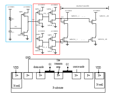 Figure. 4. ESD power clamp (IO15c) and the cross section of the stacked MOSFET
This paper compares IO15c and IO15e by using the same layout area (95um*144um), different component sizes and different methods. Because IO15e uses the substrate-driven method, it has one more mask (triple-well layer) than IO15c. IO15c’s stacked MOSFET belongs to the same substrate and the drain node can be shared, so the layout area can be reduced so the size of the stacked MOSFET is 27um/0.44um. IO15e’s first-level stacked MOSFET belongs to the same substrate and the drain node cannot be shared, whereas its second-level stacked BJT belongs to the same substrate and the drain node can be shared. Therefore, the layout area cannot be reduced and the size of the first-level stacked MOSFET is 13.5um/0.44um and the second-level stacked BJT is 27um/0.44um.
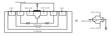 Figure. 5 Parasitic NPN junction
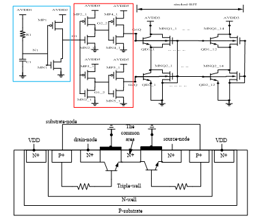 Figure. 6. ESD power clamp (IO15e) and the cross section of the stacked BJT
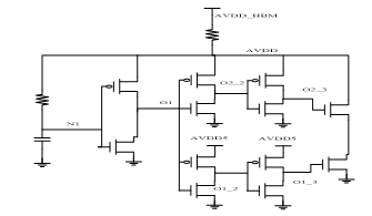 Figure. 7. ESD power clamp (IO15_HBM)
By using transient simulation, it was confirmed that the voltage of each node is lower than the junction breakdown voltage of the 3.3V device, when AVDD_HBM ranges from 0V to 3KV. The detection voltage of IO15 including nodes O1 and N1 which determines the turn-on time. Figure. 7 shows the ESD power clamp (IO15_HBM) and series resistance (1500 ohms) for carrying out HBM simulation. Because the ESD power clamp (IO1) uses the RC-transient detector to drive large dimensions (BIGFET), and the ESD power clamp (IO15) uses the RC-transient detector to drive small dimensions of the delay-line, the turn-on time of IO15’s detection point N1 is faster than the ESD power clamp (IO1) [5]. From the simulation results, AVDD is 12V, which is lower than the junction breakdown voltage, and the turn-on time of detection point N1 is 150ns for the ESD power clamp (IO15). The diagram of AVDD, N1, ad O1 versus time is shown in Figure. 8. Moreover, when the ESD event disappears, all the IO1 and IO15 devices are turned off. Based on the simulation results, the total leakage current of both the ESD power pad (IO1) and the ESD power pad (IO15), with a typical process corner and a temperature of 25°C, are 464.4pA and 197.05pA, respectively. The ESD power clamp (IO15) has a lower rate of current leakage than the ESD power pad (IO1), and the stacked structure of the leakage current is smaller than that of the BIGFET.In addition, in order to meet the specification of the sensor system, the size of the stacked MOSFETs ESD clamp (IO15c) is resized three times to achieve a larger-than-HBM ESD level of 4.5KV. The final measurement result of stabilized voltage, to reduce the leakage current that increases with temperature, is 1.0V. The original ESD clamp (IO15c) was changed to the ESD clamp (IO15c_resize).
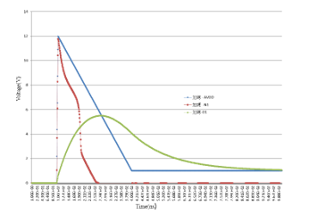 Figure. 8. IO15_HBM simulation results
4. Measurement results and discussion
Both IO15c and IO15e have the same layout area (95um*144um), and compares with different methods include the gate-driven method and two-level–driven with both the gate-driven substrate-driven methods, respectively.
The ESD power clamp (IO15c/IO15e/IO15_resize) is fabricated by the UMC 0.18um 1P6M CMOS-MEMS process; all devices use a 3.3V device. Figure. 9 shows VDD-VSS with a Positive mode and verifies the ESD level from VDD to VSS. Table 2 shows the ESD power clamp (IO15c/IO15e/IO15_resize) ESD test including HBM/MM for VDD to VSS with a Positive mode, the leakage current temperature of 25°C/125°C, the layout area, and the turn-on time when the VDD pin is zapped by a pulse [5], [6]. In addition, Figure. 10(a), 10(b) shows the turn-on time versus voltage, current of the ESD power clamp (IO15c_resize)—the turn-on time is about 160ns when the VDD pin is zapped by a pulse and the ESD current is led away. For the electrical measurements of the (IO15c_resize), the I‑V characteristics and leakage currents versus AVDD are shown in Figure. 11(a). The (IO15_resize) leakage current versus AVDD when VDD ranges from 0.5V to 1.5V and the temperature is 25°C is shown in Figure. 11(b).
 Figure. 9. VDD-VSS with Positive mode
Table 2. The ESD power clamp (IO15c/IO15e/IO15_resize) ESD test
| IO15c | IO15e |
IO15c _resize |
|
| turn-on time | 160ns | 160ns | 160ns |
| leakage current at temperature of 25 ℃ /125 ℃ when AVDD3 is 1.0V |
3.5pA/ 16.45nA |
2.8pA/ 16.89pA |
|
| leakage current at temperature of 25 ℃ /125 ℃ when AVDD3 is 1.8V |
4.75pA/ 16.98nA |
3.81pA/ 17.41nA |
|
| HBM with Positive | 8KV | 5.5KV | 8KV |
| MM with Positive | 600V | 300V | 1000V |
| layout area(um*um) | 95*144 | 95*144 | 95*387 |
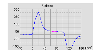 Figure.10. (a) The IO15c_resize turn-on time versus voltage when the VDD pin is zapped by a pulse
 Figure.10. (b) The IO15c_resize turn-on time versus current when the VDD pin is zapped by a pulse.
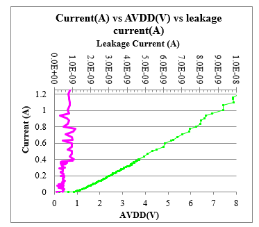 Figure. 11. (a) I-V characteristics of leakage current versus AVDD (IO15c_resize)
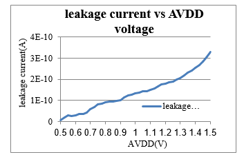 Figure. 11. (b) leakage current versus AVDD (IO15c_resize)
According to the measurement results, the ESD power clamp (IO15c/IO15e/IO15_resize) has a lower rate of current leakage and power consumption. It is expected to have less impact on and be suitable for ultra-low power sensor system applications. The proposed design has an HBM ESD level with a Positive higher than 8KV, 5.5KV, 8KV, and the MM level protection with a Positive higher than 1000V, 300V, 600V MM ESD level. The proposed design for IO15c consumes 3.5pA/16.45nA at temperatures of 25°C/125°C when AVDD3 is 1.0V, and consumes 4.75pA/16.98nA at temperatures of 25°C/125°C when AVDD3 is 1.8V. The proposed design for IO15e consumes 2.8pA/16.89nA at temperatures of 25°C/125°C when AVDD3 is 1.0V, and consumes 3.81pA/17.41nA at temperatures of 25°C/125°C when AVDD3 is 1.8V. In addition, the proposed design includes an IO15c_resize, which consumes 132.8pA at a temperature of 25°C when AVDD3 is 1.0V. The leakage current of the IO15c_resize is larger than originally expected. The reason is that it is connected to the overall ESD protection circuit and affected by other ESD protection circuits. The layout area is 13680/13680/41040 . Figure. 10 shows a dye photo of the ESD power clamp (IO15c/IO15e). Table 3 shows the ESD power clamp (IO12[9]/IO15c/IO15e/IO15_resize) ESD test including HBM/MM for VDD to VSS with a Positive mode, leakage current, layout area, and turn-on time when the VDD pin is zapped by a pulse. The measurement data was reported by Integrated Service Technology Incorporated and Agilent 3458A.From the analysis of the measurement results, IO15c/IO15c_resize can be achieved higher than an HBM/MM ESD level of 4.5KV/400V by using the gate-driven method. IO15c can even shrink to 70~80% to achieve optimization. IO15e cannot reach an HBM/MM ESD level of 4.5KV/400V because the first-level gate-driven of the IO15e is effective, but the second-level substrate-driven of the IO15e does not have a full effect. Moreover, the common area is too small and the distance between the drain junction and the source junction is too close, so that a complete effective parasitic NPN junction or a complete stacked BJT cannot be formed. The solution to this issue is that a stacked BJT cannot share a drain junction, instead the parasitic NPN junction uses its own triple-well to isolate itself to achieve the stacked-BJT. However, the layout area will be larger than that of the IO15c, and an additional layer of triple-well is required, which is not cost-effective.
Table 3. The ESD power clamp (IO12/IO15c/IO15e/IO15c_resize) ESD test
|
IO12 [9] |
IO15c | IO15e |
IO15c _resize |
|
| turn-on time | 160ns | 160ns | 160ns | |
| leakage current at temperature of 25 ℃ /125 ℃ when AVDD3 is 1.0V |
3.5pA/ 16.45nA |
2.8pA/ 16.89pA |
||
| leakage current at temperature of 25 ℃ /125 ℃ when AVDD3 is 1.8V |
24pA/ 66nA |
4.75pA/ 16.98nA |
3.81pA/ 17.41nA |
|
| HBM with Positive | 4.5KV | 8KV | 5.5KV | 8KV |
| MM with Positive | 400V | 600V | 300V | 1000V |
| layout area(um^2) | 44800 | 13680 | 13680 | 41040 |
 Figure. 12. Dye photo of whole-chip ESD protection and IO15c/e
Acknowledgments
The authors appreciate the UMC and Taiwan Semiconductor Research Institute (TSRI), Taiwan, for supporting the CMOS chip manufacturing.
- J. Walraven, J. M. Soden, E. Cole, D. M. Tanner, and R. E. Anderson, “Human body model, machine model, and charge device model ESD testing of surface micromachined microelectromechanical systems (MEMS),” in 2001 EOS/ESD, pp. 236-246.
- J. A. Walraven, J. M. Soden, D. M. Tanner, P. Tangyunyong, E. I. Cole Jr., R. E. Anderson, and L. W. Irwin, “Electrostatic discharge/electrical overstress susceptibility in MEMS: A new failure mode,” in Micromachining and Microfabrication, 2000, pp. 30-39.
- H. R. Shea, A. Gasparyan, H. B. Chan, S. Arney, R. E. Frahm, D. Lopez, S. Jin, and R. P. McConnell, “Effects of electrical leakage currents on MEMS reliability and performance,” IEEE Trans. Device Mater. Rel., vol. 4, no. 2, pp. 198-207, 2004.
- W. D. Greason, “Analysis of charge injection processes including ESD in MEMS,” J. Electrostat., vol. 66, no. 11-12, pp. 602-608, 2008.
- M. D. Ker, “Whole-chip ESD protection design with efficient VDD-to-VSS ESD clamp circuits for submicron CMOS VLSI,” IEEE Trans. Electron Devices, vol. 46, no. 1, pp. 173-183, Jan. 1999.
- M. D. Ker, T. Y. Chen, C. Y. Wu, and H. H. Chang, “ESD protection design on analog pin with very low input capacitance for high-frequency or current-mode applications,” IEEE J. Solid-State Circuits, vol. 35, no. 8, pp. 1194-1199, Aug. 2000.
- J. Li, R. Gauthier, S. Mitra, C. Putnam, K. Chatty, R. Halbach, and C. Seguin, “Design and characterization of, a multi-RC-triggered MOSFET-based power clamp for on-chip ESD protection,” in 2006 Electrical Overstress/Electrostatic Discharge Symposium, pp. 179-185.
- M.-D. Ker, T.-Y. Chen, and C.-Y. Wu, “Substrate- triggered ESD clamp devices for use in power-rail ESD clamp circuits,” Solid-State Electronics, vol. 46, no. 5, pp. 721-734, 2002.
- Y. P. Chen, Y. Lee, J. Y. Sim, M. Alioto, D. Blaauw, and D. Sylvester, “45pW ESD clamp circuit for ultra-low power applications,” in Proc. IEEE 2013 Custom Integrated Circuits Conf.