
A Resolution-Reconfigurable Asynchronous SAR ADC with Segmented and Non-Binary Weighted Capacitance DACs
Volume 5, Issue 2, Page No 665-672, 2020
Author’s Name: Chih-Hsuan Lina), Kuei-Ann Wen
View Affiliations
Department of Electronic Engineering, University of National Chiao Tung (NCTU), Hsinchu 300, Taiwan
a)Author to whom correspondence should be addressed. E-mail: shsuanhsuan.ee01g@g2.nctu.edu.tw
Adv. Sci. Technol. Eng. Syst. J. 5(2), 665-672 (2020); ![]() DOI: 10.25046/aj050282
DOI: 10.25046/aj050282
Keywords: resolution-reconfigurable, asynchronous SAR ADC, segmented and non-binary weighted

Export Citations
With the addition of thing of internet applications to 5G smartphones, mobile standby time and ultra-low-power sensing systems have become increasingly important. Nowadays, such sensing systems typically reduce power consumption to microwatts. This paper presents segmented and non-binary weighted capacitance DACs, low power, high resolution, an asynchronous clock, a spark-detect, vcm-based switching and direct switching, and reconfigurable 9- to 12-bit DACs to meet different sensing system applications. Multi-voltage is used to achieve microwatt-level power consumption. The analog/digit voltage is 1.5V/0.9V, respectively and can adjust the 4-mode resolutions (9/10/11/12 bits). The performance of the SNDR achieves 50.78, 58.53, 62.42, and 66.51db, respectively and consumes 2.69uW and results in a figure of merit (FoM) of 30.4fJ/conversion step for 12-bit mode.
Received: 07 Janury 2020, Accepted: 03 April 2020, Published Online: 17 April 2020
1. Introduction
This paper refers to the previous paper titled “A Resolution-reconfigurable SAR ADC with Partially Thermometer Coded DACs.” [1] The Internet of Things uses multi-sensors recently. Using CMOS MEMS process to integrate different electronic systems are more and more frequent. The electronic system can reduce power consumption and maintain high-efficiency operations, which have always been important issues. The 3-axis CMOS MEMS accelerometer are capacitive sensors and capacitive sensitivities often less than 1fF/g. The circuit of the readout need to own a variable conversion gain of the capacitance to voltage to meet different needs. The circuit of the readout include a gain amplifier, correlated double sampling (CDS) and chopper, and a programmable gain amplifier (PGA). The readout circuit adopts time division multiplexing to reduce power consumption, and the output voltage of the three-axis accelerometer is given to the asynchronous SAR ADC with segmented and non-binary weighted capacitance DACs. This paper chooses a low power, high resolution, internally generated asynchronous clock, using a thermometer code to segment capacitors of the higher bits and improve the linearity for 3 MSB (the most significant bit), non-binary weighted DAC capacitance array for lower bits to avoid incomplete settle issues caused error and increase error correction capabilities, a spark-detect schematic to avoid meta-stability issues, vcm-based switching and direct switching methodology to reduce the switching average energy and delay time, and uses negative voltage switch to adjust the resolution (12/11/10/9 bits), increase linearity and reduce leakage for reconfigurable resolutions. However, the average switching energy of the segment capacitance DAC array architecture is the same with Merged capacitor switching (MCS) and less than either the monotonic capacitor array or a conventional capacitor array architecture. [2]
2. Successive approximation register analog-to-digital converter architecture
2.1. The analysis of the The architecture of the vcm-based switching architecture
Figure 1 shows the architecture of the vcm-based switching. The following is the operation process of the vcm-based switching architecture. The capacitance DAC array on the top plate and positive side of the bootstrapped switch to the input signal Vip switches. The common-mode voltage Vcm (common-mode voltage) switch to the bottom plate capacitor. In the next phase, the input signal (Vip) float, and the comparator can collect the node voltages (vxp & vxn) and make decision directly and does no switch any capacitor. The S10p (MSB) is high when the input voltage Vxp is greater than Vxn. The maximum capacitor on bottom plate and the positive side switch from Vcm to Vref, and the maximum capacitance on the bottom plate and negative side switch from Vcm to GND. The SAR ADC will duplicate this procedure until the least significant bit (LSB) make decision. Figure 2 shows the vcm-based switching functional flow diagram.
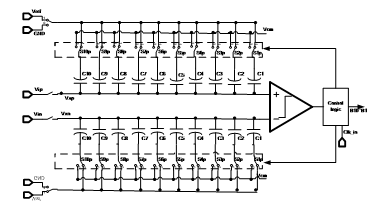 Figure 1. The architecture of the vcm-based switching
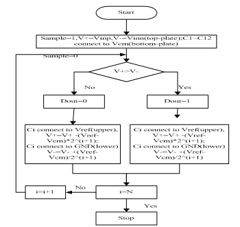 Figure 2. Vcm-based switching functional flow diagram
This paper proposes a new architecture use segmented capacitance DAC array for higher bits (3 bits) and non-binary weighted capacitance DAC array for lower bits (11 bits). In addition, using the architecture of differential to eliminate the effect of substrate noise and power noise to meet 12-bit accuracy. The ratio of all the capacitance DAC array is (256:256:256:256:256:256:256:112:64:32:20:10:8:4:2:2:1:1). The higher bits (3 bits) divides the capacitor into 7 capacitors, each . The segmented capacitance DAC array use a thermometer code to segment and reduce the mismatch caused by the capacitor. Then the lower bits (11 bits) uses the non-binary weighted methodology. When the ADC which used binary weighting capacitance DAC array is in conversion state, external or internal interference maybe causes error decision and degrades the ADC’s performance. This paper of the SAR ADC uses a non-binary weighted methodology and has 2 more cycle operations than binary weighted methodology. It can continue to correct ADC digit representation by using excess 2 cycle operations. Figure 3 shows vcm-based switching architecture with both segmented and non-binary weighted capacitance DAC array.
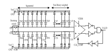 Figure 3. Vcm-based switching architecture with both segmented and non-binary weighted capacitance DAC array
Moreover, the formula of the average switching energy of the vcm-based switching architecture for this paper is “(1)” and 341 , which is smaller than the conventional switching method and the monotonic switching method. On the other hand, the number of switches is 4(n+2) and the number of unit capacitors is which is also smaller than the conventional switching method. [3,4]
 2.2. Analysis of linearity
To make the lower bits of the SAR ADC has no quantization error, every split capacitor keeps “radix of 2” form. The non-binary weighted of the lower bits is (112:64:32:20:10:8:4:2:2:1:1) and 112C is , 20C is , 10C is , 2C is . The higher bits are implemented with 7 identical capacitor size which is . The advantage of the DAC with thermometer coded is that it can make the higher bits have better linearity and DNL. The analysis of linearity is as follows.The non-binary weighted capacitor array, each weighted capacitance can be expressed as [1][5]![]()
where i is an integer representing bit position, is the error term, is unit capacitor, Dn is the digital output, n is the number of bits, y is the digital output.
then, subtracting both the no error term of the nominal value and the error term of the . The error term is expressed as follows
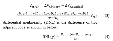
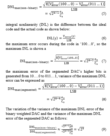
the maximum error is generated from 10….0 to 011…1, variance of the maximum DNL error can be expressed as
3. ADC Architecture Design
3.1. System architecture
Figure 4 shows the system architecture of the SAR ADC with segmented and non-binary weighted capacitance DACs. It is divided into analog part and digit part. The analog part includes bootstrap switch, comparator, the negative voltage switch, and negative voltage level shifter, the negative voltage switch power generator. The digit part includes the vcm-based switching and bit register control logic, an asynchronous clock, error correction schematic, and voltage level shifter. The digit part use VDDL (0.9V) and analog part use VDDH (1.5V) to save power and negative voltage NEG_H2(-1.5V). The segmented capacitor DAC array has 3 bits and non-binary weighted capacitor DAC array has 11 bits. The capacitor DAC array include capacitor array and switch. Moreover, the resolution scale (RS) control uses RS_I[1] and RS_I[0] to generate RS0~2 and control the negative switch on positive side and negative side of DAC capacitance array, includes mux and a negative voltage switch. Both the power and ground of the negative switch on DAC capacitance array’s positive side are VDDH and VIP+NEG_H2 and the negative side are VDDH and VIN+NEG_H2. The VIP and VIN are input signal. In addition, the voltage level shifter uses the contention mitigated level shift (CMLS) architecture [6] and the unit capacitance uses 9fF. Figure 4. The system architecture of the SAR ADC with segmented and non-binary weighted capacitance DACs
3.2. Sample and hold
Figure 5 shows the bootstrap switch, which performs the function of the sample-and-hold. Then the input signal (VI) achieves near the full range and can suppress the signal distortion to greater than 12 bits. [7] The operation of the bootstrap switch is shown in Figure 6. When CLKS is high, the voltage of the node VG fix at the voltage VDDH + VI to make the on-resistance of M10 keeps a small constant value, which can improve the linearity, reduce the significant distortion. When CLKS is low, the VG is low and M7&M10 turns off. From the simulation, the sample rate of 50Ks/s and get 8192 sample points in the Nyquist input frequency. Then taking fast Fourier transformations (FFT) for the bootstrap switch connect to the output load capacitor 18pf. The signal to noise and distortion ratio (SNDR) of sample-hold is 87.2db and an effective number of bits (ENOB) is 14.29.
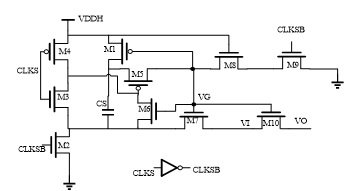 Figure 5. The bootstrap switch
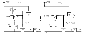 Figure 6. The operation of the bootstrap switch
3.3 Segmented control logic/RS control logic/negative voltage switch/negative power generator
Figure 7 shows the proposed segmented capacitance DAC array, non-binary weighted capacitance DAC array, and resolution scalable (RS). The vcm-based switching control logic for segmented capacitance DAC array use 3- to 7-bit binary-to-thermometer logic to divided into 7 equals capacitances, and the T is 3. Moreover, the RS control logic uses 2- to 3-bit binary-to-thermometer decoder to generate RS0~RS2 and control the negative voltage switchs on top plate of DAC capacitance array for higher bits. The 3- to 7-bit binary to thermometer code conversion logic expression is as follows.
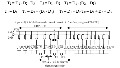 Figure 7. The segmented and non-binary capacitance DAC array on positive side
The negative voltage switch with both high linearity and low leakage is SW (M16&M17). Figures 8 and Figures 9 show the negative voltage switch schematic and operation. When SW turn off, CTRL is VI +NEG_H2, and CTRLB is VDDH. When SW is on, CTRL is VDDH, and CTRLB is VI + NEG_H2. This uses VDDH (1.5V) and VO2 (VI + NEG_H2) as the control switching power supply generated from the negative power generator and VI comes from VIP and VIN. Thus, the negative voltage switch has high linearity and low leakage characteristics. Because VO2 (VI + NEG_H2) can maintain, the junction voltage of SW (M16&M17) remains less than 1.8V, and SW (M16&M17) are 1.8V components. Therefore, SW can contribute less parasitic capacitance to the capacitance DAC array. Moreover, Figure 10 shows the negative power generator of the negative voltage switch. When VDDH is ready, the START_x is pulled from low to high, and both START_x signal and CLK11 generate the START signal through “and gate” and negative voltage level shifter. When START is low, the M11 is off to make the NEG_H2 voltage store in capacitor CB2, and the voltage of VO is VDDH. When START is high, the M11 is turn-on to make sure the VI signal is formed from the capacitance DAC array, and VO is VI + NEG_H2. The voltage of VO generates VO2 through the unit gain buffer and generates the power supply of the negative switch. The control signal (RS_I) of the negative switch generates both CTRL and CTRLB through the VDDH and VO2 to control SW (M16&M17). All components are 3.3v devices except SW (M16&M17). Then the negative voltage NEG_H2(-1.5V) can be generated by the charge pump circuit method. Figure 13 shows the timing of the negative power generator.
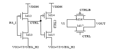 Figure 8. The negative voltage switch schematic with both high linearity and low leakage
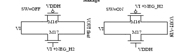 Figure 9. The negative voltage switch schematic with high linearity and low leakage operation.
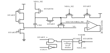 Figure 10. The negative power generator for the negative voltage switch
The negative voltage level shifter uses the CMLS architecture. It has smaller power consumption and delay than the conventional level shifter. As Figure 11 shows, all the schematics of the negative voltage level shifter are 3.3v devices. Both the VDDH and NEG_H2 are 1.5V/-1.5V, respectively.
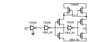 Figure 11. Schematic of the negative voltage level shifter [6]
3.4. Asynchronous clock/multi-phase clock/phase generator/vcm-based switching and bit register control logic/spark-detect/error correction
The previous paper describing the SAR ADC uses the synchronous clock cycle to complete the conversion state as follows. After sampling, the SAR ADC enters the conversion step of the N cycle. At the rising edge of each clock cycle, the comparator compares the voltage of both the capacitor DAC array’s positive (vxp) and negative sides (vxn). At the falling edge of each clock cycle, the comparator resets the voltage and enters the initial state. This action continues until the N clock cycle. From the comparator comparison to the comparator reset, each clock cycle is designed to be the same time. Because the comparison time of the comparator is related to the input voltage difference, when the input voltage difference is less than 1LSB, the comparator will require a longer comparison time. When the comparison time exceeds the clock cycle which is designed to be the same time, this will cause poor DAC settle time and degrade ADC performance. In addition, for N-bits SAR ADC, it takes N + 1 clock cycle to complete the conversion time, and an additional clock generator is required. To solve these problems, this paper uses an internally generated asynchronous clock to control the signal. The sampling rate is the clock rate, so the extra clock generator can be omitted. The asynchronous clock can adjust the length of each clock cycle in different environment due to internal circuit’s delay and comparator. When the input voltage difference is larger than 1LSB, the comparator will have a shorter comparison time, and the clock cycle is shorter. In contrast, the input voltage difference is less than 1LSB, and the clock cycle is longer. This allows more time to poor DAC settle time and save time from fast DAC settle time.
The asynchronous clock generation process is as follows: The voltages of vxp and vxn pass the comparator to generate VO_P1 and VO_N1. The differential signals (VO_P1 and VO_N1) can form VALID signal via inverter, “nand gate”. Then the VALID signal merges CLKS and CLK11 generates CLKC via “nor gate”. Moreover, CLKC passes the delay line to increase the duty cycle of the asynchronous clock and form CLK_COMP. The CLK_COMP signal is the feedback control generated by internal circuit and the comparator. As Figure 12 shows, the generated clock cycle can be used to compare and reset its own state, and it can also be used to trigger vcm-based switching and bit register control logic.
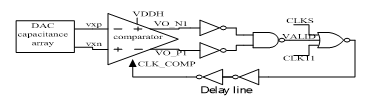 Figure 12. Asynchronous clock of this paper of the SAR ADC
When the sampling signal (CLKS) and the asynchronous clock signal (CLKC) is ready, the asynchronous clock signal (CLKC) controls vcm-based switching and bit register control logic generates the multi-phase clock, CLK0_3, CLK0_2, CLK0_1, and CLK1~CLK11. Then the CLK11 signal will reset the node voltage of all the blocks of successive approximation register analog-to-digital converter to avoid wasting power. Figure 13 shows the timing diagram of the successive approximation register analog-to-digital converter. The multi-phase clock is represented as CLKi and ~CLKi is CLKi plus inverter. The number of i represent different multi-phase clock which are 0_3~0_1 and 1~11. The bit register control logic of the previous paper uses a synchronous clock signal to trigger D-flip-flop to generate the multi-phase clock and then uses D-flip-flop to switch the capacitance DAC array’s switch. [8] The bit register control logic of this paper is both the voltage of vxp and vxn of the capacitance DAC arrays that pass the comparator and inverter gate to generate OCMP_P and OCMP_N and are controlled by the asynchronous clock (CLKC). The OCMP_P and OCMP_N signals go directly to the latch of the bit register control logic, as Figure 14 shows. This latch is dynamic logic and controlled by CLKS, ~CLKi-1, and PHASEBi, as Figure 15 shows. The PHASEBi signal is used to control the latch and turn off and save power after the work is completed. Then it generates the corresponding digital outputs (LOLi and LORi) and enters the vcm-switching control logic to switch the specified capacitor of the capacitance DAC array. In addition, the phase generator is controlled and generates PHASEBi by CLKS, CLKi, and CLKi-1, as Figure 16 shows. Because the latch is dynamic logic, the delay time of the bit register is smaller than that of the previous version.
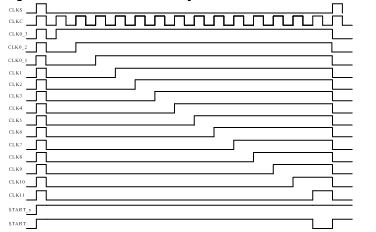 Figure 13. The timing diagram of the successive approximation register analog-to-digital converter
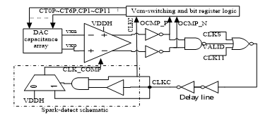 Figure 14. Vcm-based switching and bit register control logic and spark-code detect schematic
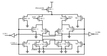 Figure 15. Latch
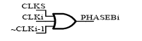 Figure 16. Phase generator
The asynchronous clock signal (CLKC) control bit register control logic generates the multi-phase clock. Using multi-phase clock triggers the vcm-based switching logic, and the output (LOLi and LORi) of the latch enters the vcm-based switching control logic. Then the output of the vcm-based switching logic generates CT0~CT6 for higher bits and CP1~CP11 for lower bits. The vcm-based switching control logic timing diagram for lower bits is as follows: when CLKi is low, CPi is Vcm (common-mode voltage). Moreover, when CLKi is high, CPi is Data_in and CNi is ~Data_in. The Data_in may be Vref or GND. This action is repeated until the end of the lower bits. The vcm-based switching control logic timing diagram for higher bits is as follows: when CLK0_3/CLK0_2/CLK0_1 is 0/0/0, the CT6~CT0 is 0000000, and the CT6~CT0 from Vcm switches to GND. When CLK0_3/ CLK0_2/CLK0_1 is 1/0/0, the CT6~CT0 is 0001111, and the CT6~CT4 switches from Vref to GND and CT3~CT0 switches from Vcm to Vref. Moreover, when CLK0_3/CLK0_2/CLK0_1 is 1/1/1, the CT6~CT0 is 1111111, and the CT6~CT0 switches from Vcm to Vref. Figure 17(a), 17(b) shows the vcm-based switching control logic timing diagram for higher bits and lower bits.
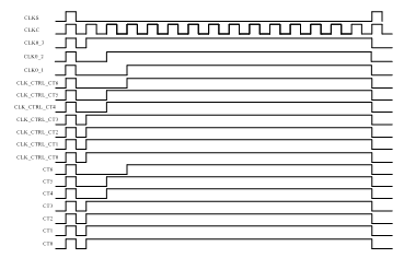 Figure 17(a). Vcm-based switching control logic timing diagram for higher bits Figure 17(b). Vcm-based switching control logic timing diagram for lower bits
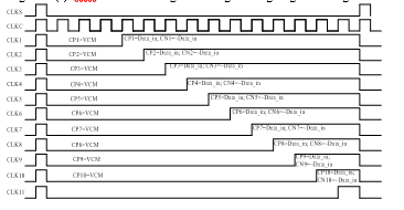
Figure 17(b). Vcm-based switching control logic timing diagram for lower bits
The previous paper uses a binary weighted capacitor array for lower bits. In the first cycle, the capacitance DAC array of both the positive side (vxp) and the negative side (vxn) enter the differential input of the comparator. When the voltage of the positive side is larger than the voltage of the negative side, the output of the comparator is high. Then the output of comparator enters vcm-based switching and bit register control logic and generate the corresponding output to control the capacitance DAC array. In the next cycle, the voltages of both vxp and vxn are reduced by a factor of 2. The ADC continues this process until the end of the N-bits cycle. Finally, the difference of both the ADC digit representation and the input analog signal should be less than 1LSB. When there is thermal noise or supply noise that affects ADC, the ADC will have an incomplete settle caused error. Finally, the difference of both the ADC digit representation and the input analog signal may be greater than 1LSB. To solve the issue, this paper uses a non-binary weighted capacitance DAC array. In the first cycle, the action is as same as binary weighted capacitance DAC array. In the next cycle, the voltage of both vxp and vxn are reduced from 256 to 112, not a factor of 2. The ratio of the capacitance DAC array for lower bits is (112: 64: 32: 20: 10: 8: 4: 2: 2: 1: 1) and 2 more cycles than the capacitance DAC array for lower bits of the binary weighted capacitance DAC array. When there is thermal noise or supply noise that affects ADC during the conversion cycle, the voltage on the positive and negative sides of the capacitance DAC array will be reduced by the capacitance DAC array ratio in each bit cycle. The ADC can continue to correct ADC digit representation by using excess 2 cycle operations until the N+2 cycle ends. Finally, the difference of both the ADC digit representation and the input analog signal should be less than 1LSB. Then the output digital level of SAR ADC is converted to 12 bits through error-correction schematic. Figures 18 and 19 show the error-correction schematic and error-correction algorithm for higher bits and lower bits.
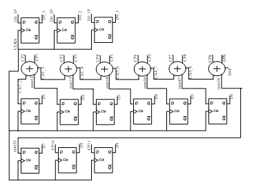 Figure 18. The error-correction schematic for higher bits and lower bits Figure 19. The error-correction algorithm
 Figure 19. The error-correction algorithm
In addition, the comparator has a meta-stability issue. When the input voltage difference is less than 1LSB and close to zero, the comparator will take a longer comparison time. If the comparison time is larger than the sample rate and not determined, the ADC output digit code will generate a large error (sparkle codes). This issue is caused by the occasional inability of the comparator. To solve this issue, the spark_detect schematic is designed. The CLKC form CLK_COMP through buffer and mux. When the input voltage difference is less than 1LSB and close to zero, the comparator will take a longer comparison time. When the comparison time exceeds 4us and the comparator is not determined, the spark_detect is low and CLK_COMP is high, which will make the comparator reset to the initial state and then continue to the next comparison until the N+2 cycles are completed. The entire process loses 1~2 cycles, but there are still other cycles that can perform the comparison cycle to reduce the residual voltage that is the different voltages of both vxp and vxn and reduce the spark-code probability. Figure 14 shows the spark_detect schematic.
3.5. Scalable voltage design
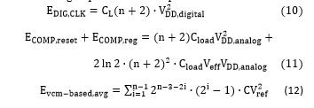
This paper uses multi-voltage to reduce power consumption and can be divided into two parts, include an analog part and a digital part. The level shifter is the bridge between the analog block and the digit block. Scaling down the supply voltage is a way to lower energy. The supply voltages of the analog block and digit block are 1.5V and 0.9V, respectively. The formula of the energy-per-conversion is “(10)”. The CL(n+2) is the effective load “capacitance, and is the supply voltage of the digital part. The comparator energy-per-conversion, which are in a cycle of comparison and reset, can be derived as “(11)”. [9,10] The n-bit SAR ADC needs n+2 comparison and reset cycles per conversion, the Cload is the comparator’s capacitive load, Veff is the overdrive voltage of the transistor, and the is the analog part’s power supply. The Vcm-based average switching energy is shown in Formula “(12)”, and the average switching energy is proportional to the transistor overdrive voltage squared and the capacitor dimension.
 3.6 Comparator
The comparator consists of two stages, as Figure 20 shows. The preamp of the first stage has a fixed current source (M5) and the second stage of the voltage amplifier and a latch make the output reach near full range. The offset voltage of the two differential end (VIP&VIN) of the comparator is classified to static offset and has no influence with the accuracy, but it will reduce the input range and the signal-to-noise ratio. Using a Monte Carlo simulation and add offset in the input differential pair (M1&M2), the SNR decreases slightly, and the effect of ENOB is little influenced.
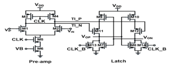 Figure 20. comparator [11]
4. Measurement and Discussion
This paper includes segmented and non-binary weighted capacitance DAC array, bootstrap switch, segmented control logic, RS control logic, negative voltage switch, asynchronous clock, vcm-based switching and bit register control logic, spark-detect, error correction, scalable voltage, comparator. The measurement results are described as follows. The input frequency is at the Nyquist rate and the maximum sampling rate is 50 KS/s. Then the output waveform gets 65536 points for the Fast Fourier Transform (FFT) analysis. The supply voltage of analog part is at 1.5V and the supply voltage of digital part is at 0.9V. The clock duty cycle is 22% and the clock period is 20us. The reconfigurable SAR ADC has 4 modes (12/11/10/9 bits), and the corresponding effective number of bits (ENOB) is 10.76/10.22/9.43/8.14 bits in the Nyquist input frequency (fin) and fin is 25/25/25/25 KS/s, respectively. The power of the SAR ADC of this paper is 2.69uW for 12-bit mode and does not include the negative power generator. Table I shows the comparison of the SAR ADC results. Moreover, the input sine waveform with frequency 9.17968Khz, the sampling rate is 50Khz, and the number of sampling points is 65536. Then the sine waveform obtained is differential linearity(DNL) +0.82LSB/-0.25LSB and integral linearity(INL) +0.9LSB/-0.62LSB, as figure 21 shows. The measurement data was reported by Taiwan Semiconductor Research Institute (TSRI).
Table I: Comparison of the SAR ADC results
| [11] | [12] | The previous of the synchronous clock | This paper of the asynchronous clock | |
| Resolution | 10 bits | 12 bits | 12 bits | 12 bits |
| Technology(um) | 0.13 | 0.18 | 0.18 | 0.18 |
| Supply voltage (V)(Analog/Digital) | 1.0/0.4 | 1.8/ | 1.8/0.9 | 1.5/0.9 |
| Area (mm2) | 0.19 | 2.38 | 0.35 | 0.35 |
| Sampling Rate (KS/s) | 1 | 200 | 50 | 50 |
| SNDR (dB) | 56.54 | 69.6 | 68.6 | 66.51 |
| Power (uW) | 0.05 | 41.5 | 9.7 | 2.69 |
| FoM (fJ/conversion) | 94.5 | 84.6 | 88.4 | 30.4 |
From the measurement results, the ENOB of the SAR ADC has lost 0.4 to 0.7 bits for different resolutions. From comparison both the measurement result and simulation result of the INL and DNL, there are 0.2 to 0.4 LSB difference for 12-bit mode. The reason is that the ground part of the power supplier is disturbed by external noise. The solution is to use the linear regulator with ultra-low-noise to generate an independent power supply to the SAR ADC of this paper. Figure 21. The DNL and INL of the SAR ADC of this paper.
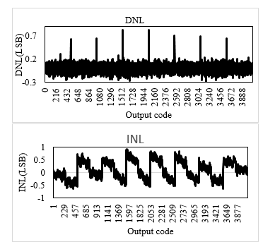 Figure 21. The DNL and INL of the SAR ADC of this paper
The layout of the DAC capacitor array is placed by a common-centroid method and add the dummy capacitors are around the DAC capacitor array to decrease the influence of process variation. The overall layout area is 810um x 430 um. Figure 22 shows the layout plan of the SAR ADC ,including the segmented DAC capacitor array for higher bits, non-binary weighted DAC capacitor array for lower bits, negative voltage switch, comparator, sample-and-hold (S/H), and switch and bit register control logic, error correction.
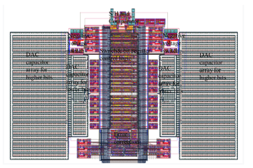 Figure 22. A resolution-reconfigurable asynchronous SAR ADC with segmented and non-binary weighted DACs layout plan
Acknowledgment
The authors appreciate the United Microelectronics Corporation (UMC) and Taiwan Semiconductor Research Institute (TSRI), for supporting the CMOS chip manufacturing.
- V. Hariprasath, J. Guerber, S. H. Lee, and U. K. Moon, “Merged capacitor switching based SAR ADC with highest switching energy-efficiency,” Electron Lett., vol. 46, no. 9, pp. 620-621, 2010.
- Yuan-Fu Lyu, “A low power 10-Bit 500-KS/s delta-modulated successive approximation register analog-to-digital converter for implantable medical devices,” M.S. thesis, Institute of Electronics, National Chiao Tung University, Hsin Chu, 2012.
- C. C. Liu, S. J. Chang, G. Y. Huang, and Y. Z. Lin, “A 10-bit 50-MS/s SAR ADC with a monotonic capacitor switching procedure,” IEEE J-Solid St Circ., vol. 45, no. 4, pp. 731-740, 2010.
- S. Haenzsche and R. Schüffny, “Analysis of a charge redistribution SAR ADC with partially thermometer coded DAC,” in 2013 European Conference on Circuit Theory and Design, 2013, pp. 1-4.
- C. Q. Tran, H. Kawaguchi, and T. Sakurai, “Low-power high-speed level shifter design for block-level dynamic voltage scaling environment,” in 2005 International Conference on Integrated Circuit Design and Technology, 2005. ICICDT 2005., 2005, pp. 229-232.
- S. Wang and C. Dehollain, “Design of a rail-to-rail 460 kS/s 10-bit SAR ADC for capacitive sensor interface,”” in 2013 IEEE 20th International Conference on Electronics, Circuits, and Systems, 2013, pp. 453-456.
- H.-M. Lin and K.-A. Wen, “A low power reconfigurable SAR ADC for CMOS MEMS sensor,” in SoC Design Conference, 2017, pp. 7-8.
- M. Yip and A. P. Chandrakasan, “A resolution-reconfigurable 5-to-10-bit 0.4-to-1 V power scalable SAR ADC for sensor applications,” IEEE J-Solid St Circ., vol. 48, no. 6, pp. 1453-1464, 2013.
- Z. Dai, C. Svensson, and A. Alvandpour, “Power consumption bounds for SAR ADCs,” in 2011 20th European Conference on Circuit Theory and Design, 2011, pp. 556-559.
- D. Zhang, A. Bhide, and A. Alvandpour, “A 53-nW 9.1-ENOB 1-kS/s SAR ADC in 0.13-mm CMOS for medical implant devices,” IEEE J-Solid St Circ., vol. 47, no. 7, pp. 1585-1593, 2012.
- Y. H. Juan, H. Y. Huang, S. C. Lai, W. H. Juang, S. Y. Lee, and C. H. Luo, “A Distortion Cancelation Technique With the Recursive DFT Method for Successive Approximation Analog-to-Digital Converters,” IEEE Transactions on Circuits and Systems II: Express Briefs, vol. 63, no. 2, pp. 146-150, 2016.