
Analysis of Two-Dimensional Electron Gas Formation in InGaAs-Based HEMTs
Volume 5, Issue 2, Page No 597-605, 2020
Author’s Name: Itsuki Takagi, Takuma Kato, Hirohisa Taguchia)
View Affiliations
Department of Electrical and Electronic Engineering, School of Engineering, Chukyo University, Nagoya, 4668666, Japan
a)Author to whom correspondence should be addressed. E-mail: htaguchi@sist.chukyo-u.ac.jp
Adv. Sci. Technol. Eng. Syst. J. 5(2), 597-605 (2020); ![]() DOI: 10.25046/aj050275
DOI: 10.25046/aj050275
Keywords: 2 DEG, InGaAs HEMTs, Potential shape

Export Citations
In this study, a theoretical simulation was performed using the Schrodinger-Poisson method to elucidate the formation factors for two-dimensional electron gas in InGaAs-based HEMTs. No visible change was observed in the carrier density and the potential shape. The inflection point of the energy level and the agreement of the energy level in each dimension were confirmed for the change in the number of carriers in the channel layer. It was found that the number of electrons at this coincidence point almost coincided with the number of electrons in the IV characteristics measured by the previous research for each gate voltage. The change in carrier state suggested that a 2DEG was formed. In addition, by considering the transport of carriers on the crystal lattice plane as a cause of the inflection point of the energy level, it was suggested that it might be caused due to the occurrence of the degeneracy process at a certain moment. From these results, it was experimentally and theoretically shown that the formation of 2DEG was caused by the carrier degeneration and the state change.
Received: 06 March 2020, Accepted: 31 March 2020, Published Online: 10 April 2020
1. Introduction
The InGaAs crystal is a ternary compound semiconductor known for forming the channel layer of a high electron mobility transistor (HEMT) [1]-[3]. Generally, the HEMT structure is constructed by using a heterojunction with a heterogeneous semi-conductor crystal. For this reason, band discontinuity occurs at the crystal surface bonding interface. Furthermore, in the electrostatic potential caused by the space charge under thermal equilibrium, band bending occurs [4], [5]. Thus, an electron transport layer called a two-dimensional electron gas (2DEG) is formed in the channel layer [5]. As an advantage of the 2DEG formation, transmitted electrons are hardly scattered by impurities, and excellent high-speed transmission with low noise is obtained [6, 7]. Research on the characteristics such as the high-speed transmission and low noise in HEMTs has been performed on InGaAs crystals as well as on HEMTs that combine other materials [8]-[10].
However, there are few reports on the principle of 2DEG formation. Due to the formation principle of 2DEG, the quantum size effect (quantum confinement effect) has been reported [11], [12]. This is a phenomenon that occurs when the carriers are confined in a widened region spanning the de Broglie wave. It is often used as an explanation for a low-dimensional structure for the 2DEG interpretation in a quantum dot. This phenomenon forms the basis for creating the channel layer of a few nanometers in HEMT fabrication [13], [14].
However, we have experimentally observed the moment of 2DEG formation in InGaAs-based HEMTs as a previous study [15]. Figure 1 shows a part of the experimental result of the previous research. In this experiment, the IV characteristics were measured by setting the drain voltage applied to the device to a very small value from -0.5 mV to 4.8 mV. In addition, a decrease in the drain current was found for InGaAs-based HEMTs when irradiated with light at a wavelength of 1480 nm. From figure 1, it is evident that the drain current sharply spikes at a certain drain voltage value. In addition, the timing at which the current value rises was shifted due to its dependence on the light intensity. When the HEMT operation was viewed, high-speed operation was found at the moment of the rise of the current value, and a rapid improvement in electron transport speed was obtained. It was considered that 2DEG was formed or expressed at this moment.
From the above, it is assumed that a 2DEG is formed from at a certain moment. The explanation of the quantum size effect alone is not sufficient for the principle of 2DEG formation.
Therefore, the purpose of this study was to elucidate the formation factor of 2DEG in InGaAs-based HEMTs. A theoretical simulation was performed on an InGaAs-based HEMT; physical parameters of the device were compared with the experimental data shown in figure 1, and the factors involved in the formation of 2DEG were discussed.
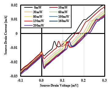 Figure 1: A part of the experimental results of the previous research.
2. Experiment Methods
2.1 Device Structure Model
A cross-sectional view of the device structure used in this expe-riment is shown in Figure 2. Theoretical calculations near the channel layer were performed from the barrier layer to the buffer layer in the simulations performed in this study. Table 1 summa-rizes the parameters for each layer.
2.2 The Schr dinger -Poisson Method
In this analysis, Wolfram Mathematica 12 was used as the theoretical calculation software. The Schrodinger-Poisson method using local density approximation in density functional theory was employed as the solver [16]. This solver calculates the parameters such as the energy level, wave function, potential function, and the carrier density function of the electron-hole system in the HEMT structure. The direction perpendicular to each layer plane was defined as the x-axis, and a one-dimensional calculation was performed. The used mathematical formulas are described below. A time-independent Schrodinger equation was introduced to describe the quantum mechanical effects that occur in the HEMT structures [17].
![]() Where ψ is the wave function, E is the energy eigenvalue, V is the potential energy, ℏ is the Dirac constant, and m* is the effective mass of electrons and holes of the target material. The solution to the Schrodinger equation gives the wave function associated with the energy. The wave function represents a spatial probability distribution indicating the presence of electrons and holes at a specific energy level. In this calculation, the carrier function defines the potential energy function. Therefore, the time dependence of the potential was not considered. Subsequently, the carrier density was calculated. The carrier density of a semi-conductor in an equilibrium state within the parabolic band approximation can be calculated from the following equation [18].
Where ψ is the wave function, E is the energy eigenvalue, V is the potential energy, ℏ is the Dirac constant, and m* is the effective mass of electrons and holes of the target material. The solution to the Schrodinger equation gives the wave function associated with the energy. The wave function represents a spatial probability distribution indicating the presence of electrons and holes at a specific energy level. In this calculation, the carrier function defines the potential energy function. Therefore, the time dependence of the potential was not considered. Subsequently, the carrier density was calculated. The carrier density of a semi-conductor in an equilibrium state within the parabolic band approximation can be calculated from the following equation [18].
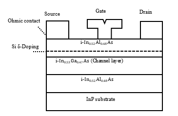 Figure 2: The cross-sectional view of the device structure used in this experiment.
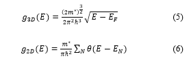
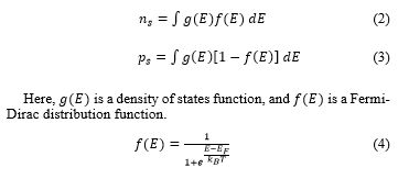 The density of states function gives the number of states per unit volume and unit energy in the -space. In this analysis, the electron and hole states in the same HEMT structure were compared in three and two dimensions.
 When calculating the carrier distribution at the target potential, the carrier distribution in the channel layer region was not uniform with the triangular wave potential in the HEMT. The band edge of the triangular potential was strongly bent at the junction interface. Therefore, a band structure was mounted on the potential of the Schrodinger equation. This forms a constraint within the domain of the wave function [19]. In this case, the square of the wave function was a probability distribution function and it represents the probability of a particle having a specific energy level in the region.
From these, the carrier density is;
 This time, in order to calculate the carrier density for a specific energy level, after performing indefinite integration, the energy eigen value of the object was substituted into the energy dependence function (state density and distribution function). Subsequently, the potential function of the HEMT structure was introduced. In this analysis, the potential function in the HEMT structure was defined by the following equation.
![]() The first term of is introduced by the Poisson equation. In this equation, the electrostatic potential is related to the space charge distribution in the system [20].
The first term of is introduced by the Poisson equation. In this equation, the electrostatic potential is related to the space charge distribution in the system [20].
 Here, represents the relative permittivity of each material, represents the permittivity in a vacuum, and represents the charge distribution of the semiconductor. In addition, is the carrier density of electrons and holes, and is the ionization dopant density by acceptors and donors.
Solving the Poisson equation defines the electrostatic potential . In addition, the band discontinuity and the exchange correlation potential are defined. The exchange correlation potential is an interpolation formula developed by Hedin and Lundqvist and plays a role to change the Schrodinger equation for one particle system into an equation for another particle. This time, the Stern and Das Sarma format was adopted [21,22].
 2.3 Calculation Method
In the simulation method, initially, a Poisson equation is calculated as a trial function. At this time, the calculation is performed under the condition that the electron and hole densities are set to 0. Thus, the well-type potential in the band offset state in the thermal non-equilibrium state was determined. The Schrodinger equation was calculated for the obtained electrostatic potential. Thereafter, the carrier density and the carrier concentration were calculated using the obtained energy eigen value and wave function. At this time, three-dimensional and two-dimensional systems were used for the density of states function. An exchange-correlation potential was defined from the obtained carrier density.
Table 1: Targeted Layers and Materials
| Target Layers | Materials | Layer Width [nm] | Doping Density [ ] | Effect of Gate Voltage [%] |
| Barrier | InAlAs | 100 | 0 | 100 (Schottky barrier) |
| Doping | InAlAs (Si doped) | 0.2 | 1.5×10²⁰ | 50 |
| Spacer | InAlAs | 20 | 0 | 50 |
| Channel | InGaAs | 15 | 0 | 25 |
| Buffer | InAlAs | 100 | 0 | 0 |
The calculation was repeated using these parameters. In this analysis, the change in potential shape due to the gate voltage was incorporated into the program, and the dependence at each gate voltage was compared. The potential function is as follows;
![]() The effect of the gate voltage on each layer was dependent on the distance from the surface of the Schottky junction (see Table 1). For the purpose of reproducing a gradually increasing electronic state, the carrier density was defined by superposition of the carrier densities obtained in each calculation. This was done to reproduce the situation of the previous study [15] in the simulation. As a result, the equations were not self-consistent and did not converge. Therefore, the convergence condition was derived from the IV characteristics obtained in previous studies as the convergence criterion for the calculation [15]. The electron concentration was calculated using the theoretical formula of the drain current in the linear region of the IV characteristic. After that, experiments and theory were compared for each obtained parameter.
The effect of the gate voltage on each layer was dependent on the distance from the surface of the Schottky junction (see Table 1). For the purpose of reproducing a gradually increasing electronic state, the carrier density was defined by superposition of the carrier densities obtained in each calculation. This was done to reproduce the situation of the previous study [15] in the simulation. As a result, the equations were not self-consistent and did not converge. Therefore, the convergence condition was derived from the IV characteristics obtained in previous studies as the convergence criterion for the calculation [15]. The electron concentration was calculated using the theoretical formula of the drain current in the linear region of the IV characteristic. After that, experiments and theory were compared for each obtained parameter.
3. Results
3.1 The shape of Potential
The potential shape of the electron-hole system is shown in figure 3. As a result of the simulation, a potential shape known as the HEMT structure was obtained. For the energy eigen values, the ground level and the second level (excitation level) were
 Figure 3: The potential shape in the electron-hole system (Vg=0).
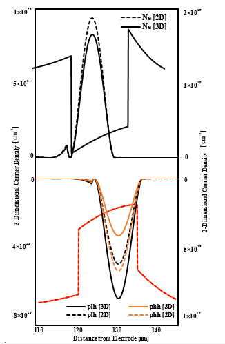 Figure 4: The carrier density distribution ).The plh means light hole density and phh means heavy hole density.2D means a 2-dimensional state, and 3D means a 3-dimensional state.
obtained as solutions for the triangular wave potential. The subsequent energy levels were found to be around 0.545 eV. This was the result of level formation in the InAlAs layer by Si doping. In the hole system, two types of heavy holes and light holes were separately simulated. No significant change was observed in the potential shape; a paired potential was formed for the electron system.
3.2 The Carrier density
The results of the carrier density distribution are shown in figure 4. In this simulation, calculations were performed by defining the density of states function as two-dimensional and three-dimensional. From figure 4, no difference in the carrier distribution was found between the two-dimensional and three-dimensional orders in the electronic system. The hole density in the two-dimensional hole system does not vary significantly. The light holes had about three times as many hole carriers as the heavy holes in the hole density of the three-dimensional system. This was considered to be due to the difference between the light and heavy hole effective mass values.
3.3 The Energy Level
The result of the dependence of the energy eigenvalue on the number of electrons was shown in figure 5. The three-dimensional energy eigen value was not affected by the quantum size effect. Therefore, the three-dimensional energy eigen values are not discretized. Figure 5 plots a total of the three energy eigen values, one energy eigenvalue in a three-dimensional system, a ground level, and an excitation level in a two-dimensional system. From figure 5, it was found that the energy eigenvalue of the three-dimensional system rapidly changed with the increase in the
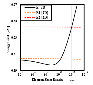 Figure 5: The dependence of the energy eigenvalue on the number of electrons.
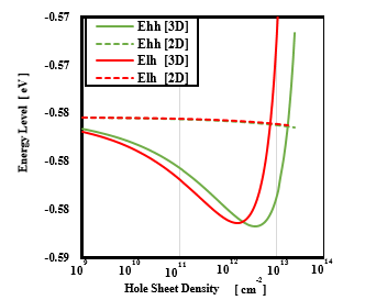 Figure 6: The dependence of the energy eigenvalue on the hole concentration.
number of electrons in the channel layer. In addition, it was found that there was an inflection point in the three-dimensional system where the energy changed from a decreasing trend to an increasing trend. Furthermore, it was observed that the energy eigenvalue of the three-dimensional system coincides with the ground level of the discrete two-dimensional system at a certain number of electrons. When comparing the number of electrons at this time with the result calculated from the IV characteristics.
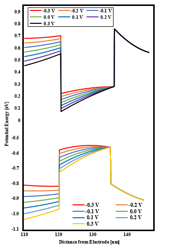 Figure 7: The potential shapes at each gate voltage.
It was found that the number of electrons almost coincided with the number of electrons at the moment when the peak was gene-rated (at the moment when the shape of the IV characteristic changed abruptly). Subsequently, the dependence of the energy eigenvalue on the hole concentration is shown in figure 6. The energy eigenvalues in the two-dimensional system were the same for both the light and heavy holes (Elh and Ehh). However, in the eigenvalues of the energy in the three-dimensional system, the existence of an inflection point was confirmed at a certain moment with the increase in the number of holes, as in the electron system. In addition, the timing at which this inflection point occurs differs between a light hole and a heavy hole. It was found that the timing deviation occurred first in the light holes and then in the heavy holes. In this simulation, the initial settings of the trial function and the quasi-Fermi level in the heterostructure were set in such a way that the hole concentrations of light and heavy holes were the same. Therefore, it was considered that the difference in the effective mass and the like, affects the hole system.
3.4 The Gate-Voltage dependence of each parameter
3.4.1 The shape of Potential
The potential shapes at each gate voltage are shown in figure 7. In the electron system, it was found that when a negative gate voltage was applied, the potential shape gradually changed to a well-shaped potential such as the band offset. It was also found that when a positive gate voltage was applied, the potential shape formed was a triangular wave potential deeper towards the electrode. The table 2 summarizes the energy eigenvalues in a two-dimensional system for each potential. As it can be seen from the table 2, it was found that the energy eigenvalues such as the ground level, also changed according to the value of the applied gate voltage. On the other hand, in the hole system, little change in shape was observed for light holes and heavy holes, resulting in a pair with the electron system. The figure 7 plots the potential shape of heavy holes.
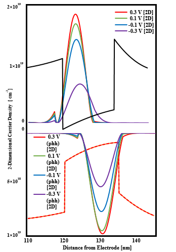 Figure 8: The carrier distribution for each gate voltage
Table 2: Summarizes the energy eigenvalues in a two-dimensional system for each potential.
| Gate Voltage [V] | Ground State [eV] |
Second Level (Excited State) [eV] |
| 0.3 | 0.14622 | 0.22147 |
| 0.2 | 0.16584 | 0.22299 |
| 0.1 | 0.18519 | 0.23293 |
| 0 | 0.20445 | 0.24296 |
| -0.1 | 0.22356 | 0.25313 |
| -0.2 | 0.24230 | 0.26366 |
| -0.3 | 0.26005 | 0.27519 |
3.4.2 The Carrier density
Subsequently, the results of the carrier distribution for each gate voltage are summarized in figure 8. In the electronic system, it was confirmed that as a negative gate voltage was applied, the electron distribution shifted toward the substrate. On the other hand, when the gate voltage was positive, the distribution did not fluctuate so much. In the case of the hole system, when the gate voltage was negative, it was found that the voltage slightly shifted to the electrode side. When the gate voltage was positive, almost no change in the hole distribution was observed as in the case of the electron system. Figure 8 plots a two-dimensional system since no change in distribution was observed in two and three dimensions.
Table 3: The electron concentration at the time of occurrence of the inflection point in the electron energy eigenvalue function at each gate voltage.
| Gate Voltage [V] |
Simulated Result (Inflection Point) |
Electron sheet Density (IV Characteristic) |
| 0.3 | 1.576 | 1.580 |
| 0.2 | 1.541 | 1.552 |
| 0.1 | 1.458 | 1.475 |
| 0 | 1.42 | 1.429 |
| -0.1 | 1.260 | 1.271 |
| -0.2 | 1.047 | 1.089 |
| -0.3 | 7.271 | 7.142 |
3.4.3 The Energy Levels
The dependence of the energy eigenvalue with the number of electrons on the gate voltage is shown in figure 9. The existence of an inflection point at a certain number of electrons for the energy eigenvalues of the three-dimensional system was confirmed under all gate voltage conditions. The table 3 shows the electron concentration at the time of occurrence of the inflection point in the electron energy eigenvalue function at each gate voltage. As shown in table 3, under all conditions, the electron number, at the moment when the peak occurs in the IV characteristic almost coincides with the electron areal density at the point indicating the inflection point in the energy eigenvalue function. Figure 10 shows the result of the energy eigenvalue with respect to the gate voltage in the hole system. The inflection point of the energy eigenvalue in the three-dimensional system was observed under each gate voltage condition. The table 4 summarizes the hole concentrations at the time of occurrence of the inflection point in the energy eigenvalue function of heavy holes and light holes at each gate voltage.
Table 4: Summarizes the hole concentrations at the time of occurrence of the inflection point in the energy eigenvalue function of heavy holes and light holes at each gate voltage.
|
Gate Voltage [V] |
Light Hole (Inflection Point) |
Heavy Hole (Inflection Point) |
Electron sheet Density (Before Rising current) |
Electron sheet Density (Rising current at Peak) |
| 0.3 | 2.036 | 4.103 | 1.580 | 2.485 |
| 0.2 | 1.749 | 3.916 | 1.552 | 2.481 |
| 0.1 | 1.577 | 3.725 | 1.475 | 2.421 |
| 0 | 1.534 | 3.590 | 1.429 | 2.275 |
| -0.1 | 1.331 | 3.387 | 1.271 | 1.981 |
| -0.2 | 1.140 | 3.168 | 1.089 | 1.811 |
| -0.3 | 7.410 | 2.906 | 7.142 | 1.531 |
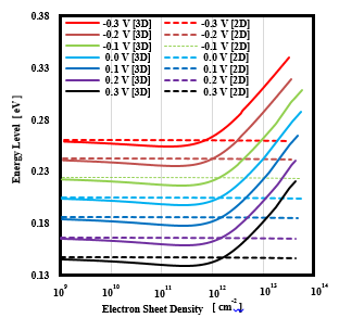 Figure 9: The dependence of the energy eigenvalue with the number of electrons on the gate voltage.
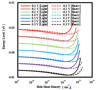 Figure 10: The energy eigenvalue with respect to the gate voltage in the hole system.
4. Discussions
4.1 The shape of Potential
From the simulation results, it was confirmed that the shape of the potential changes with respect to the gate voltage. These results suggest that the change in the Fermi level is related to the factors that cause the shape of the potential with respect to the gate voltage condition [23].
In the HEMT structure, the Fermi level of the metal electrode matches the Fermi level of the barrier layer material due to the Schottky junction between the metal electrode and the barrier layer material. Thereby, the difference between the work function and the electric affinity was formed as a Schottky barrier, and a hetero junction was established.
The gate electrode also has a Schottky junction with the barrier layer. The Fermi level of the metal electrode changes due to the minority carriers generated when a gate voltage was applied. As a result, it was considered that a potential shape change had occurred. The heterostructure was formed by a thermal equilibrium state. This means that the Fermi levels for each material and the metal electrode were the same, and the potential shape must0 have continuity [24]. The application of the gate voltage causes a change in the Fermi level on the metal electrode side and changes the Schottky barrier. In the process of changing to the non-equilibrium state, the potential in the barrier layer changes to satisfy the equilibrium state to maintain continuity. The potential shapes of the doping layer and the spacer layer, which were continuous layers, were changed accordingly.
In this simulation, the Fermi level in the device was defined using pseudo Fermi level. Therefore, it was impossible to discuss the change of Fermi level in detail. However, it is true that each energy eigen value changes with the change of the potential shape. It means that when the energy states in the device are changed, it should also cause change in the Fermi level.
4.2 The changes of Energy level
Ⅰ) In the electron system
The energy eigen value of the electron system changed from showing a decreasing tendency to an increasing tendency at a certain number of electrons. The above result suggests that in the process of forming 2DEG, the inflection point of this energy eigenvalue changes the electronic state from three-dimensional to two-dimensional.
Electrons in the channel layer try to select an energy state at a given energy level as a solution [25]. In the system simulated this time, it is an exchange correlation potential function treated as another particle system instead of one particle system. The interpretation of the obtained energy level is the minimum energy state that the electron can take. In this case, electrons have to occupy the ground level, having a low energy and most stable; it will be arranged on the reciprocal lattice point corresponding to the ground level around the energy. As a result, the electron-electron spacing becomes uniform, and the interaction between the electrons decreases. Then, it was considered that the energy value of the electrons tends to decrease. On the other hand, when the number of electrons supplied to the channel layer gradually increases, the number of electrons that can be arranged at the reciprocal lattice point around the ground level exceeds at a certain moment; the electron level starts to degenerate. As a result, the electron-electron spacing becomes non-uniform, thus the interaction between electrons is considered to increase. The results of this simulation suggest that the peak value of the number of electrons observed in the IV characteristics was due to the formation of 2DEG in the channel layer.
Ⅱ) In the hole system
It is considered that the inflection point occurs in the hole system due to the occurrence of the same phenomenon as in the electron system as described above. In this case, in the hole system, the number of holes generated in light holes and heavy holes was completely different. In the hole system, as in the electron system, the change to a two-dimensional system due to the degeneracy process is manifested by the presence of a two-dimensional hole gas (2DHG) [26], [27]. As a result of this simulation, the inflection point of the energy eigenvalue of light holes is generated during the onset of the IV characteristic (figure 1). From the results of the IV characteristics, a decrease in the drain current due to light irradiation at the forward bias can be confirmed. The current value temporarily increases due to light irradiation. However, the amount of current decrease after the IV characteristic peak value has decreased significantly as the light irradiation intensity increases. After reaching the IV characteristic peak value, the recombination ratio of electrons and holes increases. Therefore, it is suggested that the formation of 2DEG and the formation of 2DHG in the hole system promoted the recombination rate.
5. Conclusions
In this study, a theoretical simulation by the Schrodinger-Poisson method was performed to elucidate the formation factors of two-dimensional electron gas in InGaAs-based HEMTs. No significant change was observed in the carrier density and the potential shape. For the change in the number of carriers in the channel layer, the inflection point of the energy level and the agreement of the energy level in each dimension were found. It was found that the number of electrons at this coincidence point almost coincided with the number of electrons in the IV characteristics measured by the previous research for each gate voltage. The change in carrier state suggested that a 2DEG was formed. In addition, considering the transport of carriers on the crystal lattice plane as a cause of the inflection point of the energy level, it was suggested that it might be caused by the occurrence of the degeneracy process at a certain moment. From these results, it was experimentally and theoretically shown that the formation of 2DEG was caused by carrier degeneration and state change.
Conflict of Interest
The authors declare no conflict of interest.
Acknowledgment
The authors are grateful to the Chukyo University Research Found for financial assistance with this research.
- Fathimulla, A., Abrahams, J., Loughran, T., Hier, H., 1988. High-performance InAlAs/InGaAs HEMTs and MESFETs. IEEE Electron Device Lett. 9 (7), 328 – 330. DOI: 10.1109/55.733
- Behet, M., Van der Zanden, K., Borghs, G., 1998. Metamorphic InGaAs/InAlAs quantum well structures grown on GaAs substrates for high electron mobility transistor applications. Appl. Phys. Lett. 73, 2760. https://doi.org/10.1063/1.122582
- Malmkvist, M., Wang, S., Grahn, J. V., 2008. Epitaxial Optimization of 130-nm Gate-Length InGaAs/InAlAs/InP HEMTs for High-Frequency Applications. IEEE T. Electron Dev. 55 (1), 268 – 275, 2008. DOI: 10.1109/TED.2007.910613
- Newson, D.J., Merrett, R.P., Ridley, B.K., 1991. Control of gate leakage in InAlAs/InGaAs HEMTs. Electron. Lett. 27 (17), 1592 – 1593. DOI: 10.1049/el:19910996
- Rathi, S., Jogi, J., Gupta, M., Gupta, R.S., 2009. Modeling of hetero-interface potential and threshold voltage for tied and separate nanoscale InAlAs–InGaAs symmetric double-gate HEMT. Microelectron. Reliab. 49 (12),1508-1514. doi.org/10.1016/j.microrel.2009.07.044
- Thome, F., Massler, H., Wagner, S., Leuther, A., Kallfass, I., Schlechtweg, M., Ambacher, O. Comparison of two W-band low-noise amplifier MMICs with ultra-low power consumption based on 50nm InGaAs mHEMT technology. 2013 IEEE MTT-S International Microwave Symposium Digest (MTT). SEATTLE, WA, USA, DOI: 10.1109/MWSYM.2013.6697362
- Schleeh, J., Rodilla, H., Wadefalk N., Nilsson P.Å., Grahn J., 2014. Cryogenic noise performance of InGaAs/InAlAs HEMTs grown on InP and GaAs substrate. Solid State Electron.
91, 74-77. doi.org/10.1016/j.sse.2013.10.004 - Duh, K.H.G., Chao, P.C., Ho, P., Tessmer, A., Liu, S.M.J., Kao, M.Y., Smith, P.M. Ballingall, J.M. W-band InGaAs HEMT low noise amplifiers, 1990. IEEE International Digest on Microwave Symposium. Dallas Convention Center, Dallas, Texas, USA, IEEE, DOI: 10.1109/MWSYM.1990.99650
- Xu H., Sanabria C., Chini A., Keller S., Mishra U.K., York, R.A., 2004. A C-band high-dynamic range GaN HEMT low-noise amplifier. IEEE Microw. Wirel. Co. 14 (6), 262–264. DOI: 10.1109/LMWC. 2004.828020
- Yan, T., Zhang, T., Li, P., Zhang, S., 2018. Study of microwave damage effect on HEMT low noise amplifier under different drain voltage bias. Microelectron. Reliab. 82, 228-234. doi.org/10.1016/ j.microrel.2017.10.028
- Zhou, J.R., Ferry, D.K., 1993. Modeling of quantum effects in ultrasmall HEMT devices. IEEE T. Electron Dev. 40(2), 421 – 427. DOI: 10.1109/16.182523
- Krokidis, G., Xanthakis, J.P., Uzunoglu, N.K., 2008. A fully 2-dimensional, quantum mechanical calculation of short-channel and drain induced barrier lowering effects in HEMTs. Solid State Electron. 52 (5), 625-631.
doi.org/10.1016/j.sse.2007.10.021 - Taguchi, H., Kawaguchi, M., Hayakawa, M., Nakamura, Y., Iida, T, Takanashi, Y., 2006. Frequency Dependence of Drain Conductance due to Hole Accumulation in InAlAs/InGaAs High Electron Mobility Transistors. Japan J. Appl. Phys. 45 (1), 4960-4967. doi.org/10.1143/JJAP.45.4960
- Takanashi Y. “Frequency Dependence of Drain Conductance due to Hole Accumulation in InAlAs/InGaAs High Electron Mobility Transistors”, Japanese Journal of Applied Physics, Vol. 45, Part 1, pp. 4960-4967, 2006, doi.org/10.1143/JJAP.45.4960
- Taguchi H., Murakami H., Oura M., Iida T., Takanashi T., Analysis of Deviation of Threshold Voltage from Hole Accumulation Model at High Excitation, 2006, Jpn. J Appl. Phys. 45, 8549-8556. doi.org/10.1143/JJAP.45.8549.
- Takagi I., Tanabe H., Taguchi H., Analysis of the low-electron-density state of a channel layer in InGaAs High electron mobility transistors, Proceedings of International Symposium on Engineering and Applied Science, Legian Bali, Kuta, Indonesia, 238-249, 2019.
- Lyumkis E., Mickevicius R., Penzin O., Polsky B., Sayed E. K, Wettstein A., Fichtner W., Simulations of quantum transport in HEMT using density gradient model, 24th Annual Technical Digest Gallium Arsenide Integrated Circuit (GaAs IC) Symposium, Monterey, California, USA, IEEE.
doi: 10.1109/GAAS.2002.1049067. - Lin L. D., Ping Y. Z., 2006. Self-consistent analysis of double-doped InAlAs/InGaAs/InP HEMTs. Chin. Phys. 15, 2735-2741, doi.org/ 10.1088/1009-1963/15/11/046.
- Neophytou N., Rakshit T., Lundstrom S. M., 2009. Performance analysis of 60-nm Gate-Length III–V InGaAs HEMTs: simulations versus experiments, IEEE Transact Electron Devices, 56, 7, 1377-1387. doi: 10.1109/TED.2009.2021437.
- Verma N., Gupta M., Gupta R.S., Jogi J., 2013. Quantum modeling of nanoscale symmetric double-gate InAlAs/InGaAs/InP HEMT, JOURNAL OF SEMICONDUCTOR TECHNOLOGY AND SCIENCE,13, 4, 342-354. doi.org/10.5573/JSTS.2013.13.4.342
- Said T., Kelsall R. Pilgrim N., 2006. Simulation of electron transport in InGaAs/AlGaAs HEMTs using an electrothermal Monte Carlo Method, IEEE Transact. Electron Devices. 53, 8, 1768-1774, 2006. doi: 10.1109/TED.2006.877698
- Roy M., Gurman S. J., 2001. An investigation of the use of the Hedin-Lundqvist exchange and correlation potential in EXAFS data analysis. J. Synchrotron Rad. 8,1095-1102. doi.org/10.1107/S090904950100 6434.
- Nayak C., Simon H. S., Stern A., Freedman M., Sarma D.S., 2008. Non-Abelian anyons and topological quantum computation. Rev. Mod. Phys. 80, 1083-1090. doi.org/10.1103/RevModPhys.80.1083
- Taguchi H., Sato T., Oura M., Iida T., Takanashi Y., 2008. Dependence of carrier lifetime of InAlAs/InGaAs high-electron-mobility transistors on gate-to-source voltage. Jpn. J Appl. Phys. 47, 4S, 2858-2862. doi.org/10.1143/JJAP.47.2858.
- Krantz J. R., Mayer C. D., Bloss L. W., 1990. The influence of Fermi-level pinning at the GaAs substrate on HEMT threshold voltage. Solid-State Electron. 33, 9,1189-1195. doi.org/10.1016/0038-1101(90) 90098-Y.
- Yoshida H., Mozume T., Nishimura T., Wada O., 1998. Intersubband transitions in InGaAs/AlAs coupled double quantum well structures for multi-wavelength all-optical switching, Electron. Lett. 34, 9, 913-915. doi: 10.1049/el:19980605.
- Shina S.H., Park Y.H, Koob HC., Songa YH., Song J.D., 2017. GaSb/InGaAs 2-dimensional hole gas grown on InP substrate for III-V CMOS applications, Curr. Appl. Phys. 17, 7, 1005-1008. doi.org/10. 1016/j.cap.2017.03.018.