A Simple Modelling Tool for Fast Combined Simulation of Interconnections, Inter-Symbol Interference and Equalization in High-Speed Serial Interfaces for Chip-to-Chip Communications
 , Thomas Bernardi 1, Alessio Cortiula 1, Martino Dazzi 1, 2, Alessio De Prà 1, Mattia Marcon 1, Marco Scapol 1, Andrea Bandiziol 3, Francesco Brandonisi 3, Andrea Cristofoli 3, Werner Grollitsch 3, Roberto Nonis 3, Pierpaolo Palestri 1
Adv. Sci. Technol. Eng. Syst. J. 5(2), 527–536 (2020);
 DOI: 10.25046/aj050266
We describe an efficient system-level simulator that, starting from the architecture of a well-specified transmissive medium (a channel modelled as single-ended or coupled differential microstrips plus cables) and including the system-level characteristics of transmitter and receiver (voltage swing, impedance, etc.), computes the eye diagram and the bit-error rate that is obtained in high-speed serial interfaces. Various equalization techniques are included, such as feed-forward equalization at the transmitter, continuous-time linear equalization and decision-feedback equalization at the receiver. The impact of clock and data jitter on the overall system performance can easily be taken into account and fully adaptive equalization can be simulated without increasing the computational burden or the model’s complexity.
1. Introduction
This paper extends the work presented at the 42nd International Conference on Information and Communication Technology, Electronics and Microelectronics (MIPRO 2019) [1] and describes a simple and efficient tool for fast system-level simulation of high-speed serial interfaces, a topic that has received much attention in the past two decades due to its relevance in modern electronic systems: As the miniaturization of CMOS integrated circuits (IC) keeps following the path described by Moore’s law [2], the amount of components integrated onto single devices, the number of functionalities available on single ICs and their speed increases significantly every few years. Over the last decades, evidence has arisen that the major bottleneck in performance shifted from computational capabilities and the associated power consumption towards communication between different ICs [3]. In fact, many applications such as modern microprocessors, servers, micro-controllers, FPGAs, even portable devices and, recently, automotive systems require High-Speed I/O (HSIO) modules capable of handling data rates up to 128Gb/s with energies per bit as low as 1pJ [4–9]. Moreover, as in many applications chip area and pin availability pose strict design constraints, the aforementioned devices cannot support parallel I/O that would reduce the data rate of individual channels, implying that such communications need to be implemented as high-speed serial interfaces (HSSI). In the present paper, the terms HSIO and HSSI will be used interchangeably to denote high-speed serial communication devices. At multi-Gb/s data rates, performances are highly affected by impedance discontinuities in the interconnections due to PCB characteristics, presence of vias and package features; non-perfect impedance matching due to fabrication imperfections or poor compatibility for different devices; and by the dispersive nature of the transmissive medium at high frequencies [4, 10]. All these phenomena concur in causing Inter-Symbol Interference (ISI), which manifests itself as a smoothing and widening of the pulses sent along the channel so that they are superimposed to other symbols transmitted in the neighbouring unit intervals (UIs), thus increasing the Bit-Error Rate (BER) at the receiver, dramatically impairing the quality of the transmission [4,10,11].
In order to cope with this, HSIOs are required to implement complex equalization strategies, both at the transmitter or at the receiver, and in the analog, mixed-signal or digital domains [10, 12–15]. Such techniques include Feed-Forward Equalization (FFE) at the transmitter, Continuous-Time Linear Equalization (CTLE) and Decision-Feedback Equalization at the receiver [10]. FFE uses an FIR filter that applies a pre-distortion to the transmitted pulses in order to preemptively compensate for the channel distortion; CTLE comprises a peaking amplifier mainly employed to compensate for the high frequency attenuation of the channel and possibly provide additional gain control at low frequency; in DFE the history of recent received bits is stored into a shift register and used to correct the received analog signal in order to cancel ISI at the input of the slicer, either through FIR or IIR filters.
One of the main challenges in the design and implementation of such equalization techniques is the fact that HSIOs are supposed to operate on a variety of channels whose features are unknown at design time. Thus, the optimal parameters of the equalizers cannot be precisely known and set a priori during the design phase, unless the resulting suboptimal performance can be tolerated, when it does not completely impede communication. Even in such rare cases where the transmissive medium is well known, the design itself is intrinsically dependent on process, voltage and temperature (PVT) variations and technology corners, all of which need to be counteracted by the equalizers. Therefore, calibration and adaptation strategies are required in order to find the optimal equalization parameters for the actual channel [13,15–17]. Full adaptation automatically performs such a task, and is usually implemented in the form of Sign-Sign Least-Mean Squares (SS-LMS) algorithms due to the short time required to adjust the equalization parameters and the simplicity of their realization [11,12,15,16,18–21].
Moreover, HSIOs are also equipped with algorithms for clock and data recovery (CDR), and even performance monitoring, hence making up very complex electronic systems [12,22]. Such a complexity cannot be conveniently handled through transistor-level descriptions because of the extremely long simulation times that they require. Therefore, various system-level models have been proposed in the last decades to aid the design of HSSIs, mainly using statistical techniques [19, 23–26]. Such tools are very important for the initial system-level assessment in the design of chip-to-chip HSIOs for selecting design specifications such as the number of equalization taps, the amount of high-frequency content that needs to be equalized, evaluating the Signal-to-Noise Ratio (SNR) and the overall jitter that can be tolerated without degrading the BER.
The design and analysis of HSIOs comprising a variety of complex equalization techniques require efficient system-level models capable of producing fast and accurate predictions of the system behaviour. Extending the work presented in [1] and relating it with contributions from [19,27], this paper shows how fast system-level simulations of high-speed serial interfaces can be performed with a simple modular model. The paper proceeds as follows: Section 2, starting from the architecture of a generic HSSI, describes the numerical model, how it evaluates performance accounting for jitter and how fully-adaptive equalization is computed; Section 3 shows some sample simulation results and comparisons with post-layout transistor-level simulations, demonstrating the capabilities of the proposed approach; finally, conclusions are drawn in Section 4.
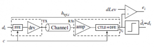
Figure 1: Scheme of a generic high-speed serial interface with equalization: htot,i is the overall pulse response of the TX (FFE+driver) + channel + RX (amplifier+CTLE+DFE) system; c is a generic equalization parameter (e.g. a filter tap), which may be either statically set or automatically adapted [19].
2. Model Description
2.1 Architecture of the Transceiver
In order to accurately model the system performance of a generic HSIO device, the general model depicted in Figure 1 and extensively described in [19] is considered: Denoting by the subscript i the sampling instant tb = iTb (where Tb corresponds to a bit period, i.e. one Unit Interval UI), the data sequence di is sent by the differential transmitter tx at a bitrate fb = 1/Tb, optionally implementing FFE; the channel, whose sampled pulse response is hch,i, can be modelled either as two independent single-ended lines or as a coupled differential line; the receiver rx contains an amplifier, a CTLE and a DFE, and produces the analog voltage yi; the slicer makes decisions on such a voltage (dˆi = sign(yi), i.e. dˆi = 1 if yi > 0V and −1 otherwise) and its sampling point can be modified with respect to the one determined by the CDR in order to perform optimal sampling [12,19]; moreover, when performing full adaptation, the analog voltage yi is compared with a reference voltage dLev [15] to determine the error ei (i.e. the distance of the actual sample to dLev, usually defined as the desired voltage level corresponding to a ‘1’ bit), and use this information to perform adaptation. Assuming that the BER is small (either because the channel has low loss or because it is well equalized), the reconstructed data dˆi is equal to the transmitted data di.
2.2 Numerical Model of the Transceiver
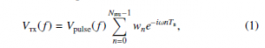
The numerical model implemented in Matlab exploits a fast approach for the modelling of ISI and equalization in HSIOs, the flowchart of which is here summarised in Figure 2 and detailed in the following paragraphs.
2.2.1 Transmitter
The idealised transmitted waveform is modelled as the trapezoidal pulse vpulse(t), shown in Figure 3a and characterised by its duration, amplitude and by the slope of its edges (rise and fall times trise = tfall); such a waveform is easily Fourier-transformed, giving Vpulse(f), to which FFE is applied by summing weighted delayed versions of the transformed pulse itself:
where wn are the weights of the Nffe FFE taps, subject to the constraint PnN=ffe0−1 |wn| = 1 due to the fact that the power available in the
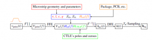
Figure 2: Diagram of the procedure implemented to obtain the received pulse response [1]. F and F−1 stand for the Fourier and the inverse Fourier transforms, respectively.
Figure 3: Example based on a PCIe 4.0 channel attenuating 20dB at 6GHz, showing the waveforms elaborated by the fast modelling tool according to the flow of
Figure 2 [1,19]. (a) shows the transmitted trapezoidal pulse vpulse(t); (b) reports the corresponding Fourier transform prior to (Vpulse(f)) and after application of FFE (Vtx(f)); (c) shows Hch(f), HCTLE(f), and the result of their multiplication with Vtx(f); (d) shows the subsequent inverse Fourier transform prior to DFE hrx(t), theapplication principle of which is shown in Figure 5.
driver is limited. The effect of such an operation is shown in the frequency domain in Figure 3b.
The proposed approach considers a transmitter’s impedance which is kept constant and does not change at high or low outputs, as is the case in Input-Output Buffer Information Specification (IBIS) models [28, 29]. Moreover, the pulse shape used in the proposed method (trapezoidal shape with trise = tfall) is chosen in order to exploit the channel’s linearity and hence use the channel’s pulse response in the various computations instead of its step response [26]; in other words, a sequence of pulses vpulse(t) having the same amplitude results in a constant voltage level, which is not the case with other pulse shapes, see [30].
2.2.2 Communication Channel
The transmissive medium is generally modelled as a differential line, made up either of two independent microstrips (to simulate lines placed at some distance from each other as to minimise interactions) or a single coupled microstrip excited with an odd mode (to realistically reproduce differential signalling). This is then used to reproduce the salient features of any other type of transmission line, such as the target attenuation at a certain frequency or its characteristics impedance.
The microstrip features are computed from the line’s geometry and material parameters following the approach defined in [31–36] for single-ended lossy microstrips, or extended to the coupled case according to [37,38], and then used to extract its per-unit-length parameters r(f), l(f), c(f), g(f) considering dielectric losses and skin effect, all of which are among the main contributors to ISI [4]. Such a result can then be combined with Hext(f), a transfer function representing the socket or package and incorporating notch filters, which can be used to take into account discontinuities, vias, etc. in order to provide a complete description of realistic channels.
| application principle of which is shown in Figure 5. | |
| driver is limited. The effect of such an operation is shown in the frequency domain in Figure 3b.
The proposed approach considers a transmitter’s impedance which is kept constant and does not change at high or low outputs, as is the case in Input-Output Buffer Information Specification (IBIS) models [28, 29]. Moreover, the pulse shape used in the proposed method (trapezoidal shape with trise = tfall) is chosen in order to exploit the channel’s linearity and hence use the channel’s pulse response in the various computations instead of its step response [26]; in other words, a sequence of pulses vpulse(t) having the same amplitude results in a constant voltage level, which is not the case with other pulse shapes, see [30]. 2.2.2 Communication Channel The transmissive medium is generally modelled as a differential line, made up either of two independent microstrips (to simulate |
lines placed at some distance from each other as to minimise interactions) or a single coupled microstrip excited with an odd mode (to realistically reproduce differential signalling). This is then used to reproduce the salient features of any other type of transmission line, such as the target attenuation at a certain frequency or its characteristics impedance.
The microstrip features are computed from the line’s geometry and material parameters following the approach defined in [31–36] for single-ended lossy microstrips, or extended to the coupled case according to [37,38], and then used to extract its per-unit-length parameters r(f), l(f), c(f), g(f) considering dielectric losses and skin effect, all of which are among the main contributors to ISI [4]. Such a result can then be combined with Hext(f), a transfer function representing the socket or package and incorporating notch filters, which can be used to take into account discontinuities, vias, etc. in order to provide a complete description of realistic channels. |
Hext(f) can be calculated with a model of the package, e.g. in terms of parasitic resistance, inductance and capacitance, which allows a straightforward evaluation of its transfer function in terms of poles and zeroes, while the contributions due to impedance discontinuities or vias can be taken into account by fitting the features of actual measurements of the transmission line’s S parameters to the transfer function of notch filters in the form
![]()
where ξ is the filter’s damping factor and f0 is its notch frequency.
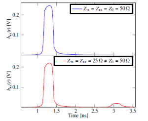
Figure 4: Effect of mismatch on the received pulse response: On top, Ztx = Zrx = Z0 = 50Ω; below, Ztx = Zrx = 25Ω, Z0 = 50Ω, showing reflections due to such a mismatch. Transmission at 4Gb/s over a low-loss channel (approximately −3dB at Nyquist frequency).
Using as additional parameters the driver’s and the receiver’s termination impedances (Ztx and Zrx, respectively), the transmission line transfer function is computed from the telegrapher’s equations as
where γ = p(r + iωl)(g + iωc) is the propagation coefficient, L is
the line length and Γtx/rx = ZZtx/rxtx/rx−+ZZ00((ff)) are the reflection coefficients corresponding to the transmitter and the receiver. Note that, due to the inclusion of Ztx/rx, (3) takes into account possible non-perfect matching among driver, transmission line and receiver, which is shown as an example in Figure 4: The mismatch produces a reflection that contributes to ISI.
2.2.3 Receiver
The CTLE is modelled as a rational function HCTLE(f) characterised by the CTLE’s poles and zeroes; optionally, an extraction of the CTLE’s transfer function from simulations of the transistor-level HSIO can be used to reproduce more accurately a realistic implementation (and the frequency response of other analog blocks in the receiver can be similarly taken into account). The received signal associated to the transmitted trapezoidal pulse has spectrum Vrx(f) , Vtx(f)Hch(f)HCTLE(f); an example of this is shown in Figure 3c with some of its sub-components.
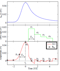
Figure 5: Procedure used by the model to apply the DFE correction to the received analog pulse response hrx(t) to obtain h(t) and eventually its sampled version heq. The DFE taps are rectangular pulses 1 UI wide and centred on the sampling point determined by the CDR.
The received pulse response h(t) at the slicer’s input is then obtained through inverse Fourier transform of Vrx(f) using the procedure in [39], yielding hrx(t) (an example of hrx(t) is shown in Figure 3d). Application of the DFE correction is performed as shown in Figure 5, i.e. by subtracting from hrx(t) rectangular pulses with amplitude equal to the tap weights ai and centred on the sampling point determined by the CDR.
The procedure above implicitly assumes that the CDR has reached its steady state and is locked. Its impact on the behaviour of the HSSI is twofold: It determines the sampling point for data, error and edge samples (which is related to the position of the “rectangles” associated to the DFE, as mentioned above), while the jitter at its output is responsible for a reduction of BER (as will be explained in Section 2.4). For what the sampling point is concerned, we can simply assume that the data samples correspond to the maximum of the pulse response h(t); alternatively, an Alexander CDR [40] can be emulated by determining the time instants corresponding to hrx,−0.5 and hrx,0.5 (which are the positions of the edge samples of the CDR in a real implementation [27]) and then assume that the data sample is exactly in between. On top of it, an algorithm for optimal sampling point may be used to determine a shift from the output of the CDR, which results in an improved sampling position [12,19]. Any of the above can be selected and all of them aim at sampling as close to the centre of the eye as possible in order to reduce the probability of error.
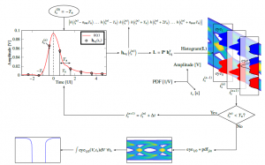
Figure 6: Diagram of the procedure used to evaluate the HSSI performance in terms of eye diagram and bathtub plot, as explained in Section 2.3. All plots and diagrams are obtained by transmitting at 12Gb/s over a channel losing 14.3dB at Nyquist frequency, with the FFE applying a de-emphasis of −2.5dB; no DFE is applied for the sake of demonstrating the working principle of the proposed method. From an initial sampling point ts(0) = −Tb, at each iteration npre + npost + 1 Tb-spaced samples of h(t) are taken to form heq ts(n); at each sampling point, histograms ofs L are computed to determine the corresponding PDFs, represented in the drawing at the top right as cross sections ofb the eye diagram; the procedure is repeated until t reaches T and then the eye diagram and bathtub plot are computed taking into account jitter at the receiver.
Sampling by the bit period Tb is eventually performed in order to obtain the analog voltages (vector heq = [h-npre … h-1 h0 h1 … hnpost ]) that would be sensed at the input of the slicer at sampling time.
2.3 Evaluating the HSSI Performance
Performances of the transceiver are determined mainly by computing the eye diagram, constructed by folding the received signal over a time length of 1UI, which allows to observe all the transitions that take place during operation of the serial link and their density; and by calculating the bathtub plot, which shows the cumulative distribution function of the received errors over the same time span of the eye diagram, indicating the sampling positions that result in an increased BER [4]. Both such metrics require probabilistic calculations in order to maintain computation times low [19,23].
From the sampled pulse response heq one can compute all possible values of the voltage yi at the samplers, due to all the possible sequences of bits that can be sent, as
![]()
where L is a column vector containing such voltage levels and P is a permutation matrix which contains all the possible bit sequences of a certain length that can be transmitted. In fact, P is structured as a truth table: It features a number of columns equal to npre + 1 + npost, where npre and npost are the number of pre- and post-cursors, respectively, which can be chosen according to their relevance in the pulse response; while the number of rows is 2npre+1+npost, i.e. the number of all possible sequences composed of npre + 1 + npost bits. In other words, L considers all the possible ways in which the samples of the pulse response can combine due to ISI, hence simulating observation of the received analog voltage yi over a sufficiently long time span. Moreover, L implicitly depends on the choice of the sampling instant ts through the sampled pulse response heq.
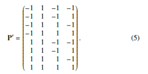
By assuming that the eye is vertically symmetric (the transceiver behaviour when transmitting a ‘1’ bit is the same as though a ‘0’ was sent, just with a sign reversal), only the cases in which dˆ = 1 are useful for the purpose of computing the HSIO performance. By coding the ‘1’ and ‘0’ bits as 1 and −1 values, respectively, and keeping only the non-redundant rows, e.g. for one pre- and two post-cursors such a reduced matrix (denoted by ’) reads
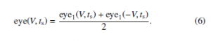
Equation (4) provides an easy way to compute the eye diagram and the bathtub plot. The eye diagram can be computed by sampling h(t) at various t = ts ∈ [−Tb/2, Tb/2], where Tb is the bit period (1 UI), and creating histograms eye1(V,ts) of the corresponding L(ts); due to the fact that the eye for the ‘0’ bit is just the flipped version of the one for the ‘1’ bit (as follows from the assumption of symmetry), they can be combined to obtain the overall eye diagram
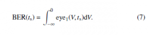
The bathtub plot, i.e. the BER corresponding to a voltage threshold equal to 0V as a function of the sampling instant ts, is then given by the probability that a ‘1’ bit is misinterpreted for a ‘0’ (that is the same as the probability that a ‘0’ bit is misinterpreted for a ‘1’, due to the above assumption of symmetry):
The overall procedure for computing the eye diagram and the bathtub plot is shown in Figure 6, summarising the flow described in this Section and in the following.
2.4 Including the Effect of Jitter
The effect of jitter on the receiver can be optionally taken into account by simply convolving the single eye1/0 of (6) and the probability density function of sampling time ts corresponding to the jitter component of interest pdfx(ts) [41]. As an example, considering an oscillator in the receiver affected by random jitter, the period jitter of which has variance σpj (in other words, a clock with phase noise going as 1/f 2, which means that the jitter values in different periods are uncorrelated) and a CDR having a bandwidth BWcdr, the squared variance of the absolute jitter present in the recovered clock can be easily shown to be given by
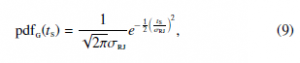
The simple example shown in Figure 7 assumes a jitter characterised by a Gaussian distribution described as
where σrj is the variance of the random jitter affecting the recovered clock as per (8), which in general may include other sources than random jitter of the clock alone.
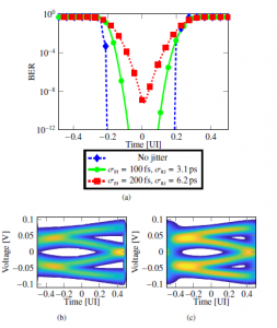
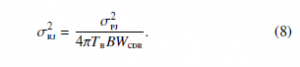
Figure 7: PCIe 4.0 channel attenuating 20dB at 6GHz; approximately 4dB of FFE de-emphasis, first 4 post-cursors cancelled by the DFE. The random jitter applied at the receiver’s recovered clock is calculated according to (8) assuming a CDR bandwidth BWcdr = 1MHz. (a) BER bathtub plots; eye diagrams with (b) no random jitter and (c) σrj = 6.2ps random jitter on the recovered clock.
2.5 Including Fully-Adaptive Equalization
As briefly mentioned in the Introduction, the problem concerning the optimal settings of the equalizers’ parameters is not trivial, and often one must resort to full adaptation in order to automatically find optimal equalization parameters. The implementation of fully-adaptive techniques based on an SS-LMS algorithm in the simulation approach described in this paper is relatively straightforward and was thoroughly described in [19]: Briefly, it involves computing quantities in the form c(k+1) = c(k) + µcsigndˆisignej, (10)
where µc is the step size, dˆ is the data sample received at time i, ej is the error at time j = i + k between the analog voltage yj at the samplers and the desired voltage dLev corresponding to a ‘1’ bit and c(k) is the k-th iteration on a generic parameter that can be adapted (the taps amplitude of FFE or DFE, the positions of poles and zeroes in a CTLE modelled e.g. as Hctle(s) = c0 + c1s, the sampling phase as well as dLev itself). Note that signdˆisignej corresponds to correlating the error made at a certain time with the bit received at possibly another time in the past or in the future, where obviously the latter can be considered only when data and errors are parallelized before computation of the fully-adaptive algorithm [8,17,27,42–44]. Such correlations provide information on whether to increase or decrease the corresponding parameter c and bring it to convergence, and are usually collected and averaged over time [12,27]. Such a correlation can be easily evaluated from heq by multiplication with a matrix similar to P0 of (5) (further mathematical details are given in [19]).
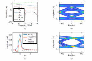
Figure 8: Simulation of a channel with 12dB attenuation at 10GHz and fixed 2-tap FFE. All the relevant Fourier transforms of signals and transfer functions of the transceiver are plotted in (a); the eye diagram prior to equalization is shown in (b); (c) shows the pulse response prior to equalization (solid blue line), after the fixed FFE (solid orange line) and after application of the fully-adaptive loop (Figure 10) and subsequent sampling (black asterisks); (d) shows the resulting equalised eye diagram.
By applying equalization to the pulse response of the transceiver plus channel, as mentioned in Section 2.2, iteration of (4) and Equation 10 provides the evolution over time of the adaptation procedure until the equalization parameters converge in the neighbourhood of the optimum [19].
3. Results
As an example of the power and versatility of the proposed approach, we consider here the fully-adaptive equalization of an HSIO transmitting at 20Gb/s with rise/fall times equal to 20% of the UI and ±0.25V differential voltage swing on a channel attenuating 12dB at 10GHz. A fixed 2-tap FFE with a pre-emphasis of approximately 6dB (w-1 = −0.25, w0 = 0.75) was applied at transmit side to reduce the first pre-cursor. The package was described by an LC π-network with L = 2nH and C = 100fF, while an impedance discontinuity was modelled by adding a notch filter with ξ = 0.1 centred at f0 = 27GHz; both features were included through the function Hext(f) mentioned in Section 2.2.2. Figure 10 shows the resulting simultaneous adaptation of dLev, CTLE’s zeroes, DFE taps and sampling phase as a function of the number of iterations performed by the fully-adaptive algorithm described above. As expected, dLev converges to the average value corresponding to the ‘1’ bit (i.e. the peak value of h(t): h0) and, as it approaches such a value, the other equalization parameters start to adapt and eventually converge: The DFE taps reach the values of the corresponding post-cursors (h1, h2 and h3), while the phase is shifted w.r.t. the position determined by the CDR to a value that zeroes the first pre-cursor. Frequency representations of all relevant signals and transfer functions of the transceiver are plotted in Figure 8a, the unequalised eye diagram is depicted in Figure 8b, the channel pulse response is shown in Figure 8c prior to equalization, after the fixed FFE and after full adaptation, a situation to which corresponds the eye diagram of Figure 8d.
In order to validate the proposed numerical model, a comparison was carried out in [27] between the eye diagram obtained with the model itself and that obtained through post-layout transistor-level simulations. An HSSI for automotive applications implemented in 28nm planar CMOS technology was simulated at 12Gb/s at transistor level with full adaptation enabled; the numerical model was then used as a comparison in terms of performance and behaviour of the SS-LMS adaptive algorithm when the HSIO was used to communicate over a realistic, high-loss channel (−33dB at 6GHz) representing a transmission line as will likely be defined by the MIPI A-PHY standard. The results of Figure 9 show a good degree of accuracy in reproducing the transistor-level simulations when relevant features of the post-layout transistor-level implementation (chiefly, the transfer functions of the CTLE and of the Variable-Gain Amplifiers in the receiver) were extracted and used in the tool, as explained in Section 2.2.3.
As a means of comparison, in order to observe convergence of with the proposed method and (b) transistor-level simulations.
Figure 9: Eye diagrams after convergence of the SS-LMS equalization loops on a MIPI A-PHY channel [27] as obtained through (a) post-processing of the pulse response
the fully-adaptive algorithm and be able to compute an eye diagram containing enough UIs, transistor-level simulations run at a speed of about 6h per µs of simulation for at least 1µs, whereas the proposed method takes about 5s to provide the results.
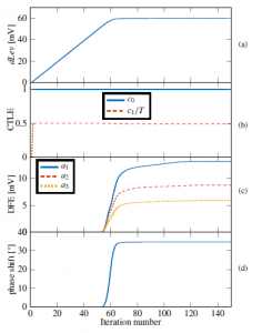
Figure 10: Simulation of a channel with 12dB attenuation at 10GHz and fixed 2-tap FFE; the trapezoidal pulse was sent at 20Gb/s bitrate, it has 20% rise/fall time and ±of (b) first-order CTLE , (c) 3-tap DFE and (d) optimal sampling point.0.25V swing differential voltage. From top to bottom, (a) dLev drives adaptation
Preliminary tests employing behavioural models for the HSSI indicate a simulation speed of about 7.3s per µs of simulation (not shown).The above is meant to be just a rough comparison, mainly because the various models do not necessarily implement all the components of an HSIO (e.g. the transistor-level simulation does not consider the digital part of the system), but it still provides some figures to consider when dealing with such kind of simulations.
4. Conclusions
We have presented a fast tool exploiting a simple modelling approach to evaluate the performance of high-speed serial interfaces for chip-to-chip communications. An efficient probabilistic algorithm was developed to evaluate the eye diagram with low computational effort. Sharing the same motivations of other similar models developed in the past in the literature, such an approach represents a powerful alternative to time-domain simulations, since complex systems working with BER as low as 10−15 require simulating very large amounts of bit periods, which may be very time consuming. The effect of the most common equalization strategies, of CDR techniques, of jitter and of full adaptation of the equalizers can be easily included in the model, so that the proposed simulation approach can be used for the system-level assessment of high-speed interfaces that need to comply with various standards. As examples of the capabilities of the proposed approach, we reported results from two interfaces: One transmitting at 20Gb/s over a relatively lowloss channel (−12dB at Nyquist frequency) and another operating at 12Gb/s over a high-loss MIPI A-PHY line (−33dB at Nyquist frequency). Both cases show that the combination of various equalization techniques is required to obtain suitable BERs, and that the proposed approach provides results that are comparable with much longer, time-domain post-layout transistor-level simulations, thus demonstrating the power of our model to evaluate the performance of realistic high-speed serial interfaces.
Conflict of Interest
The authors declare no conflict of interest.
Acknowledgement
The authors would like to thank prof. Luca Selmi (University of Modena and Reggio Emilia) for support.
- A. Cortiula, M. Dazzi, M. Marcon, D. Menin, A. Bandiziol, A. Cristofoli, W. Grollitsch, R. Nonis, and P. Palestri, “A simple and fast tool for the mod- elling of inter-symbol interference and equalization in high-speed chip-to-chip interfaces,” in The 42nd Int. Conv. on Information and Communication Tech- nol., Electronics and Microelectronics (MIPRO), Opatija, Croatia, May 2019, pp. 116–120. doi: 10.23919/MIPRO.2019.8756752.
- G. Moore, “Cramming more components onto integrated circuits,” Electronics, vol. 38, no. 8, pp. 114–117, Apr. 1965.
- H. Tamura, “Looking to the Future: Projected Requirements for Wireline Com- munications Technology,” IEEE Solid-State Circuits Mag., vol. 7, no. 4, pp. 53–62, 2015. doi: 10.1109/MSSC.2015.2477017
- T. C. Carusone, “Introduction to Digital I/O: Constraining I/O Power Consump- tion in High-Performance Systems,” IEEE Solid-State Circuits Mag., vol. 7, no. 4, pp. 14–22, Fall 2015. doi: 10.1109/MSSC.2015.2476016
- Y. Chen, P.-I. Mak, L. Zhang, and Y. Wang, “A 0.002-mm2 6.4-mW 10-Gb/s Full-Rate Direct DFE Receiver With 59.6Channel Loss at Nyquist Frequency”, IEEE Trans. Microw. Theory Techn., vol. 62, no. 12, pp. 31073117, Dec. 2014. doi: 10.1109/TMTT.2014.2360697.
- N. J. Endo, “Wireless Communication In and Around the Car: Status and Outlook. ES3: High-Speed Communications on 4 Wheels: What’s in Your next Car?” in 2013 IEEE Int. Solid-State Circuits Conf. Dig. of Tech. Papers, Feb. 2013, pp. 515–515. doi: 10.1109/ISSCC.2013.6487598.
- J. Kim et al., “A 112 Gb/s PAM-4 56 Gb/s NRZ Reconfigurable Transmitter With Three-Tap FFE in 10-nm FinFET,” IEEE J. Solid-State Circuits, vol. 54, no. 1, pp. 29–42, 2019. doi: 10.1109/JSSC.2018.2874040
- J. Lee, K. Park, K. Lee, and D.-K. Jeong, “A 2.44-pJ/b 1.62–10-Gb/s Receiver for Next Generation Video Interface Equalizing 23-dB Loss With Adaptive 2-Tap Data DFE and 1-Tap Edge DFE,” IEEE Trans. Circuits Syst. II, vol. 65, no. 10, pp. 1295–1299, Oct. 2018. doi: 10.1109/TCSII.2018.2846677
- Z. Toprak-Deniz, J. E. Proesel, J. F. Bulzacchelli, H. A. Ainspan, T. O. Dickson, M. P. Beakes, and M. Meghelli, “A 128-Gb/s 1.3-pJ/b PAM-4 Transmitter With Reconfigurable 3-Tap FFE in 14-nm CMOS,” IEEE Journal of Solid-State Circuits, vol. 55, no. 1, pp. 19–26, Jan. 2020. doi: 0.1109/JSSC.2019.2939081
- J. F. Bulzacchelli, “Equalization for Electrical Links: Current Design Tech- niques and Future Directions,” IEEE Solid-State Circuits Mag., vol. 7, no. 4, pp. 23–31, Fall 2015. doi: 10.1109/MSSC.2015.2475996
- J. W. M. Bergmans, Digital Baseband Transmission and Recording. Springer, 1996, ch. Adaptive Reception, pp. 373–450.
- V. Balan, O. Oluwole, G. Kodani, C. Zhong, R. Dadi, A. Amin, A. Ragab, and M.-J. E. Lee, “A 15–22 Gbps Serial Link in 28 nm CMOS With Direct DFE,” IEEE J. Solid-State Circuits, vol. 49, no. 12, pp. 3104–3115, 2014. doi: 10.1109/JSSC.2014.2349992
- H. Higashi et al., “A 5-6.4-Gb/s 12-channel transceiver with pre-emphasis and equalization,” IEEE J. Solid-State Circuits, vol. 40, no. 4, pp. 978–985, Apr 2005. doi: 10.1109/JSSC.2005.845562
- S. Palermo, S. Hoyos, S. Cai, S. Kiran, and Y. Zhu, “Analog-to-Digital Converter-Based Serial Links: An Overview,” IEEE Solid-State Circuits Mag., vol. 10, no. 3, pp. 35–47, Aug. 2018. doi: 10.1109/MSSC.2018.2844603
- V. Stojanovic´ et al., “Autonomous dual-mode (PAM2/4) serial link transceiver with adaptive equalization and data recovery,” IEEE J. Solid-State Circuits, vol. 40, no. 4, pp. 1012–1026, Apr. 2005. doi: 10.1109/JSSC.2004.842863
- H.-J. Chi, J.-S. Lee, S.-H. Jeon, S.-J. Bae, Y.-S. Sohn, J.-Y. Sim, and H.-J. Park, “A Single-Loop SS-LMS Algorithm With Single-Ended Integrating DFE Re- ceiver for Multi-Drop DRAM Interface,” IEEE J. Solid-State Circuits, vol. 46, no. 9, pp. 2053–2063, Sep. 2011. doi: 10.1109/JSSC.2011.2136590
- J. Savoj et al., “Wideband flexible-reach techniques for a 0.5-16.3Gb/s fully-adaptive transceiver in 20nm CMOS,” in Proc. of the IEEE 2014 Custom Integrated Circuits Conf. IEEE, Sep. 2014, pp. 1–4. doi: 10.1109/CICC.2014.6945980.
- S. Dasgupta, C.R. Johnson, and A.M. Baksho, “Sign-sign LMS convergence with independent stochastic inputs,” IEEE Trans. Inf. Theory, vol. 36, no. 1, pp. 197–201, Jan. 1990. doi: 10.1109/18.50391
- D. Menin, A. De Pr, A. Bandiziol, W. Grollitsch, R. Nonis, and P. Palestri, “A Simple Simulation Approach for the Estimation of Convergence and Perfor- mance of Fully-Adaptive Equalization in High-Speed Serial Interfaces,” IEEE Trans. Compon. Packag. Manuf. Technol., vol. 9, no. 10, pp. 2079–2086, Oct. 2019. doi: 10.1109/TCPMT.2019.2911177
- S. U. H. Qureshi, “Adaptive equalization,” Proc. IEEE, vol. 73, no. 9, pp. 1349–1387, Sept 1985. doi: 10.1109/PROC.1985.13298
- B. Widrow, J. M. McCool, M. G. Larimore, and C. R. Johnson, “Stationary and nonstationary learning characteristics of the LMS adaptive filter,” Proc.
IEEE, vol. 64, no. 8, pp. 1151–1162, 1976. doi: 10.1109/PROC.1976.10286 - B. Casper, “Clocking Wireline Systems: An Overview of Wireline Design Techniques,” IEEE Solid-State Circuits Magazine, vol. 7, no. 4, pp. 32–41, 2015. doi: 10.1109/MSSC.2015.2476015
- A. Sanders and J. DAmbrosia, “Designcon 2004 channel compliance testing utilizing novel statistical eye methodology,” 2004.
- G. Balamurugan, B. Casper, J. Jaussi, M. Mansuri, F. O’Mahony, and J. Kennedy, “Modeling and Analysis of High-Speed I/O Links,” IEEE Trans. Adv. Packag., vol. 32, no. 2, pp. 237–247, May 2009. doi: 10.1109/TADVP.2008.2011366
- D. Oh, J. Ren, and S. Chang, “Hybrid Statistical Link Simulation Technique,” IEEE Trans. Compon. Packag. Manuf. Technol., vol. 1, no. 5, pp. 772–783,
May 2011. doi: 10.1109/TCPMT.2011.2118209 - J. Ren and K. S. Oh, “Multiple Edge Responses for Fast and Accurate System Simulations,” IEEE Trans. Adv. Packag., vol. 31, no. 4, pp. 741–748, Nov. 2008. doi: 10.1109/TADVP.2008.2002201
- D. Menin, A. Bandiziol, W. Grollitsch, R. Nonis, and P. Palestri, “Design and Simulation of a 12 Gb/s Transceiver with 8-Tap FFE, Offset-Compensated Samplers and Fully-Adaptive 1-Tap Speculative/3-Tap DFE and Sampling Phase for MIPI A-PHY Applications,” IEEE Trans. Circuits Syst. II, 2019. doi: 10.1109/TCSII.2019.2926152. [Online]. Available: https://ieeexplore.ieee.org/document/8752403/
- G. Signorini, C. Siviero, M. Telescu, and I. S. Stievano, “Present and future of I/O-buffer behavioral macromodels,” IEEE Electromagn. Compat., vol. 5, no. 3, pp. 79–85, 2016. doi: 10.1109/MEMC.0.7764256
- J. N. Tripathi, V. K. Sharma, and H. Shrimali, “A Review on Power Supply Induced Jitter,” IEEE Trans. Compon. Packag. Manuf. Technol., vol. 9, no. 3, pp. 511–524, Mar. 2019. doi: 10.1109/TCPMT.2018.2872608
- A. Cristofoli, P. Palestri, N. D. Dalt, and L. Selmi, “Efficient Statistical Simu- lation of Intersymbol Interference and Jitter in High-Speed Serial Interfaces,” IEEE Trans. Compon. Packag. Manuf. Technol., vol. 4, no. 3, pp. 480–489,
Mar. 2014. doi: 10.1109/TCPMT.2013.2282530 - M. Dazzi, P. Palestri, D. Rossi, A. Bandiziol, I. Loi, D. Bellasi, and L. Benini, “Sub-mW multi-Gbps chip-to-chip communication Links for Ultra-Low Power IoT end-nodes,” in 2018 IEEE Int. Symp. on Circuits and Syst. (ISCAS), May 2018. doi: 10.1109/ISCAS.2018.8351893 pp. 1–5.
- E. Denlinger, “Losses of Microstrip Lines,” IEEE Trans. Microw. Theory Techn., vol. 28, no. 6, pp. 513–522, Jun. 1980. doi: 10.1109/TMTT.1980.1130112
- W. Getsinger, “Microstrip Dispersion Model,” IEEE Trans. Microw. Theory Techn., vol. 21, no. 1, pp. 34–39, Jan. 1973. doi: 10.1109/TMTT.1973.1127911
- E. Hammerstad and O. Jensen, “Accurate Models for Microstrip Computer- Aided Design,” in MTT-S Int. Microwave Symp. Dig., vol. 80. MTT006, 1980. doi: 10.1109/MWSYM.1980.1124303 pp. 407–409.
- M. Kirschning and R. Jansen, “Accurate model for effective dielectric constant of microstrip with validity up to millimetre-wave frequencies,” Electron. Lett., vol. 18, no. 6, p. 272, 1982. doi: 10.1049/el:19820186
- H. Wheeler, “Transmission-Line Properties of a Strip on a Dielectric Sheet on a Plane,” IEEE Trans. Microw. Theory Techn., vol. 25, no. 8, pp. 631–647, Aug. 1977. doi: 10.1109/TMTT.1977.1129179
- M. Kirschning and R. Jansen, “Arguments and an accurate model for the power-current formulation of microstrip characteristic impedance,” Archiv der elektrischen U¨ bertragung: AEU¨ , vol. 37, pp. 108–112, mar 1983.
- M. Kirschning and R. Jansen, “Accurate Wide-Range Design Equations for the Frequency-Dependent Characteristic of Parallel Coupled Microstrip Lines,” IEEE Trans. Microw. Theory Techn., vol. 32, no. 1, pp. 83–90, Jan. 1984. doi: 10.1109/TMTT.1984.1132616
- T. Brazil, “Causal-convolution – a new method for the transient analysis of linear systems at microwave frequencies,” IEEE Trans. Microw. Theory Techn., vol. 43, no. 2, pp. 315–323, Feb. 1995. doi: 10.1109 90
- Alexander, J.D.H., “Clock recovery from random binary signals,” Electron.
Lett., vol. 11, no. 22, pp. 541–542, Oct. 1975. doi: 10.1049/el:19750415 - V. Stojanovic´ and M. Horowitz, “Modeling and analysis of high-speed links,” in Proc. of the IEEE 2003 Custom Integrated Circuits Conf., 2003. IEEE, 2003, pp. 589–594. doi: 10.1109/CICC.2003.1249467.
- G. R. Gangasani et al., “A 32 Gb/s Backplane Transceiver With On-Chip AC-Coupling and Low Latency CDR in 32 nm SOI CMOS Technology,”
IEEE J. Solid-State Circuits, vol. 49, no. 11, pp. 2474–2489, Nov. 2014. doi: 10.1109/JSSC.2014.2340574 - J. Han, Y. Lu, N. Sutardja, K. Jung, and E. Alon, “A 60Gb/s 173mW receiver frontend in 65nm CMOS technology,” in 2015 Symp. on VLSI Circuits (VLSI Circuits), June 2015, pp. C230–C231. doi: 10.1109/VLSIC.2015.7231268.
- T. Shibasaki et al., “A 56Gb/s NRZ-electrical 247mW/lane serial-link transceiver in 28nm CMOS,” in 2016 IEEE Int. Solid-State Circuits Conf. (ISSCC). IEEE, Jan. 2016, pp. 64–65. doi: 10.1109/ISSCC.2016.7417908.