Improvement of the Natural Self-Timed Circuit Tolerance to Short-Term Soft Errors
 , Anton Nikolaevich Kamenskih 2, Yuri Georgievich Diachenko 1, Yuri Vladimirovich Rogdestvenski 1, Denis Yuryevich Diachenko 1
Adv. Sci. Technol. Eng. Syst. J. 5(2), 44–56 (2020);
 DOI: 10.25046/aj050206
The paper discusses the features of the implementation and functioning of digital self-timed circuits. They have a naturally high tolerance to short-term single soft errors caused by various factors, such as nuclear particles, radiation, and others. Combinational self-timed circuits using dual-rail coding of signals are naturally immune to 91% of typical soft errors classified in the paper. The remaining critical soft errors are related to the state of the dual-rail signal, opposite to the spacer and forbidden in traditional dual-rail coding of signals. Paper proposes to consider this state as the second spacer and to indicate it as a spacer to increase the self-timed circuit tolerance to soft errors. Together with an improved indication of the self-timed pipeline, this provides masking of 100% of the considered typical soft errors in combinational self-timed circuits. Due to internal feedback, self-timed latches and flip-flops are less protected from soft errors, as are synchronous memory cells. But thanks to their indication and the input and output signals generation discipline, they are also immune to 89% of typical soft errors. Usage of the self-timed latches and flip-flops with dual-rail coding of information outputs increases the tolerance of self-timed latches and flip-flops to soft errors by 2%. Application of the DICE-like approach to circuitry and layout design of sequential self-timed circuits provide an increase in their tolerance to the single soft errors up to the level of 100%.
1. Introduction
The failure-tolerance of digital integrated circuits depends, firstly, on their complexity and aging mechanisms of their components, and secondly, on the impact of a number of the destabilizing factors (noise on power and signal nets, radiation, heavy charged particles (HCP), protons, neutrons traveling through the semiconductor bulk, and others). The first type of factors leads to catastrophic failures of the CMOS integrated circuits. The second type of factors can also lead to catastrophic failures as the latch-up effect. Still, much more often, they cause short-term soft errors.
This paper discusses the natural properties of self-timed (ST) circuits, providing their high tolerance to soft errors, and proposes methods for increasing this tolerance. It is an extension of work initially presented in the 10th IEEE International Conference on Dependable Systems, Services, and Technologies, DESSERT’2019 [1].
The Single Event Transient (SET) of the digital cell (which in combinational CMOS circuits is a short-term event) is the most common [2]. A change of the memory cell state (Single Event Upset, SEU) is also possible. If the last event occurs in the memory cell storage phase, it becomes permanent rather than short-term. The duration of the failure depends on the cause of it. In this article, we consider failures caused by the passage of a nuclear particle. Depending on the particle’s energy, they last up to units of nanoseconds [3].
There are various circuitry methods for protection against soft errors. For example, Dual Data Stream Logic memory cells [4], two-phase logic cells [5], Dual Interlocked Storage Cell [6], combinational parts duplication [7], doubling each transistor in a schematic circuit [8], detection and fault isolation [9], applying additional gates [10], and so on. These solutions use the doubled or redundant implementation of circuit logical functions. There are many known techniques for improving the fault tolerance of synchronous and asynchronous circuits, for example, [11, 12], and even at the circuit synthesis level, for example, [13].
ST circuits [14 – 18] are alternative to synchronous circuits. They are initially hardware redundant, as the failure-resistant synchronous circuits are. The first reason for such redundancy is the usage of redundant code, which is mainly dual-rail one with a spacer. Secondly, ST circuits indicate the outputs of all their cells and implement a two-phase operation discipline. Such a circuit provides an increased soft-error tolerance in comparison with synchronous and even asynchronous counterparts.
The purpose of this paper is to evaluate the natural ST circuit tolerance to soft errors and suggest ways to increase it. The ST circuits analyzed in the paper belong to the quasi delay insensitive (QDI) class. They use dual-rail coding of the information signals and two-phase operation. They indicate the switching completion of all fired cells of the ST circuit in both phases of its operation. The articles and studies known to us do not contain, to our knowledge, the results of a quantitative analysis of QDI circuit tolerance to soft errors. The results of this analysis presented here are the main contribution of the paper.
The scientific novelty of this paper consists of two ideas.
The first idea is to indicate a usually forbidden state of the dual-rail signal, which is opposite to its spacer, as the correct spacer. As a result, this forbidden state becomes non-critical and does not corrupt processed data.
Another idea is to use RS-latches and RS-flip-flops with dual-rail output with spacer for storing any data. They improve ST sequential circuit tolerance to soft errors.
2. Features of ST circuits
Dual-rail coding replaces each information signal X with a dual-rail signal (DRS) {X, XB}. Usually, DRS has two working states (“01” and “10”) and one spacer. Spacer can be either zero (“00”) or a unit (“11”). The state opposite to spacer, called “anti-spacer” (AS), is prohibited in traditional ST circuits. Considering AS never appears, the classic ST indication interprets it as a valid working state (VWS). So, when it appears, for example, as a result of SET, it propagates along the circuit and corrupts data.
In addition to DRS, the ST circuits use single-rail signals – indication signals and control ones. Indication signals are generated by indication subcircuits and acknowledge the completion of the ST circuit switching into a working or spacer phase. Indication subcircuits consist of C-elements or hysteretic triggers (H-triggers) [16]. They regulate the interaction between ST parts of a total ST circuit. Therefore, we have to consider the impact of soft errors on the operation of the ST circuits with DRS and single-rail signals, which are internal and output signals for this circuit. The inputs of this ST circuit are always the output signals of some other one.
Request-acknowledge procedure for units connected by information signals (handshake procedure) accompanies a two-phase operation discipline. Each ST circuit allows switching sources of its inputs to a working (or spacer) phase only itself completes turning to a spacer (or working) phase [16]. Therefore, the ST circuit discipline masks a short-term soft error, which duration is less than the time for forming a new working state at the ST circuit outputs. Therefore, soft error criticality for the ST circuit operation depends on the time when the failure occurs within the operation cycle of the ST circuit. However, in high-performance digital ST circuits, the time factor ceases to play a decisive role.
ST sequential circuits (STSC) consist of bistable cells (BSC), which are analogs of synchronous RS-latches with cross-connections. BSC outputs form a signal having two static working states and one dynamic transit state through which the BSC passes when switching between static working states. At the absence of soft errors, its outputs at any time are in the working state (“10” or “01”) or transit state (“00” for the BSC on NOR cells or “11” for the BSC on NAND cells). The inverse state of the transit state (let’s call it “anti-transit state,” ATS) never occurs during regular operation.
A soft error occurred in an STSC can lead to irreversible consequences if it causes switching BSC to an opposite working state. In contrast to the combinational circuit, BSC has positive feedback due to cross-connections. Therefore, when BSC inputs are inactive, a soft error in one half of BSC can force switching its second half as well. As a result, the BSC latches an invalid working state (IWS) and can’t return itself to a VWS.
The difference between STSCs and combinational ST circuits also lies in their indication. STSC indication checks if BSC outputs and its inputs match in a working phase. Therefore, not all soft errors are critical.
As a result of soft errors in the source circuit, the following conditions may appear on the DRS inputs of the combinational ST circuit, not corresponded to the ST signal discipline:
- AS at one or more DRS inputs in a working or spacer phase,
- A spacer at one or more DRS inputs in a working phase,
- A working state at one or more DRS inputs in a spacer phase,
- IWS at one or more DRS inputs in a working phase.
Their duration depends on the time of natural or forced elimination of both factors:
- Soft error cause (e.g., the noise on communication wires and power stripes),
- Physical effects of the failures (e.g., an ionization current of the excess carriers injected by the traveled particles or radiation in a semiconductor bulk).
Traditional ST methodology considers AS is a prohibited state: it can never appear during the regular ST circuit operation. Therefore, the traditional ST circuit indicators do not expect it during both phases of its operation. However, a soft error can lead to the appearance of an AS state that violates the fundamental DRS generation discipline. The AS can propagate along the data processing path if one does not mask or stop it.
In a working phase, a DRS source can switch to VWS or AS, when AS appears at its inputs. For example, DRS with zero spacer, described by a pair of logical functions:
Y = A + B,
YB = AB * BB,
switches either to the AS {Y=YB=1} at {В=0, ВВ=1}, or to the expected working state {Y=1, YB=0} at В=1, ВВ=0, when the AS {A=AB=1} appears at the inputs.
Premature switching one or more DRS inputs to the spacer in the working phase does not lead to negative functional consequences. In the worst case, the internal signals and ST circuit outputs can, after switching to the working state, again return to the spacer for a time corresponding to the soft error duration. At this, data remains uncorrupted, and the indication output does not “rattle.” But some cells in the circuit can switch three times during the working phase. Initially, they switch to the expected working state before the failure, and then back to the spacer at the soft error, and again to the expected working state after the failure ends. Collector (e.g., H-trigger or C-element) combined these failure cell indicators can also switch three times during the ST circuit operation phase.
Premature switching DRS back to the working state during the transition to the spacer phase does not cause any negative functional consequences if it corresponds to the working state in the previous working phase. Otherwise, there is a possibility of switching ST circuit outputs to an IWS, after they have already switched to the current working state acknowledged by their indicator. (Remind of that in ST circuits, the previous unit does not turn to a spacer until the subsequent unit completes switching to a working phase.)
IWS in the working phase is the least probable. It involves the simultaneous switching of both DRS parts to an opposite value, i.e., the simultaneous appearance of failure in two different logical cells driving this DRS. However, such a soft error is the most dangerous for the ST circuit operation, as the circuit actively reads and processes its input data. The circuit may, in turn, generate an IWS at its outputs.
The traditional ST circuit indicator does not mask critical soft errors of BSC outputs and the accompanying control signals, which are information and indication outputs of the STSC. So, such errors can corrupt processed data and disturb the handshake between ST units.
3. Soft errors classification in ST circuits
Let’s consider the ST circuit as a functionally complete ST unit having DRS inputs and outputs and an indication output. An external source generates DRS inputs. The indication output acknowledges the completion of switching ST circuit into the current phase. Let’s assume that the ST circuit working phase lasts for the time indication output acknowledges the completion of switching this ST circuit into the spacer. Conversely, the ST circuit spacer phase corresponds to the working state of its indication output. Then the DRS can be both in a working state and in a spacer state for some time in each ST circuit phase.
In this regard, we propose a classification of all typical soft errors in the ST circuits, shown in Figure 1. All encountered observed effects can occur in both a working phase and a spacer phase of the ST circuit. A working state into which the DRS turns because of soft error may be either the expected VWS or IWS.
An ionization pulse current generated in a semiconductor body by HCP, proton, or neutron with high enough energy is one of the typical physical soft error causes. The effective track diameter of the particle traveled through the semiconductor and induced the electron-hole pairs does not exceed one micrometer (https://habr.com/post/189066 (in Russian)). In 65-nm and below CMOS process, this corresponds to the area covering the drains and sources of the homogeneous or complementary transistors in a few logical cells. Figure 2 shows a 65-nm layout fragment, including four NOR2 cells. The plan is symmetrical. CMOS n-transistors occupy the center; p-type transistors are located at left and right. Dotted circles A1 – A4 show the effective track diameter possible positions.
 Figure 1 – Classification of the soft errors in combinational ST circuits
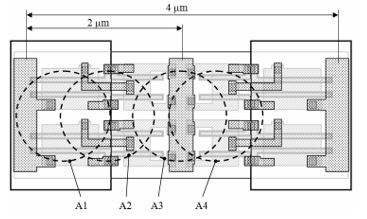 Figure 2 – Effective track diameters of the particles in the 65-nm layout
One particle cannot selectively hit, for example, only n-type transistors in one cell and only p-type transistors in another cell. It always impacts either the homogeneous transistor drains (A1, A3, A4), or the complementary transistor drains (A2) in one or several adjacent cells at the same time. Consequently, the particles affect the structure of adjacent cells symmetrically.
Thus, one traveling particle can cause ionization currents in several adjacent cells. These currents have the same direction in all impacted cells. Therefore, the potential changes at the outputs of adjacent cells have the same polarity. In the layouts with lower design rules, the effective track diameter of the impacting particle further covers the transistor drains of both types in several adjacent cells.
If the logical cells driving DRS are forcibly placed close enough to each other on a layout, the impact of particle is symmetrical. It does not cause switching these cell outputs in opposite directions. Consequently, in the CMOS ST circuits manufactured by the 65-nm process and below, existing VWS practically never turns to IWS because of any soft error.
The ST circuit response to soft errors depends on the circuit type: combinational or sequential.
The STSC consists of one (latch) or two (flip-flop) consecutive BSC, an indication subcircuit, and BSC outputs convertors into a DRS (optional). The variety of the STSCs [19] makes difficulties for analyzing all their types in one paper. So, let’s consider an STSC tolerance to soft errors by the example of ST RS-flip-flop (RSFF) shown in Figure 3. It has a DRS input {R, S} with a unit spacer, reset input (Rst), BSC output {Q, QB} with a zero-transition state (Q=QB=0), indication output (I), and consists of BSC-1, BSC-2, and indicator. BSC-1 has a unit transit state (U=UB=1).
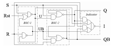 Figure 3 – ST RS-flip-flop
Figure 4 shows a classification of possible typical soft errors in ST RSFF. It includes soft errors that occur in both BSC and the indicator. For the reasons discussed above, soft error cannot lead to simultaneous switching both parts of BSC in opposite directions. Therefore, the possible occurrence of IWS is not a soft error directly. Still, it can happen as a result of the BSC transit state and the spacer at the input {R, S}.
The ST RSFF current phase is a working one if the DRS {R, S} is in the spacer. In the working phase, the RSFF information output {Q, QB} updates its state. The input {R, S} working phase corresponds to the ST RSFF spacer phase. In the spacer phase, the BSC-1 updates its state, and the BSC-2 stores its state. Note that ATS in BSC-1 causes the BSC-2 to store its state.
Let’s examine the possible soft errors in combinational ST circuits and RSFFs in more detail and evaluate the probability of data corruption in the ST circuit due to them. In the first approximation, we consider the possible cases in each analyzed situation to be equally probable. Let’s call the reason, caused the soft error, by the term “bug.”
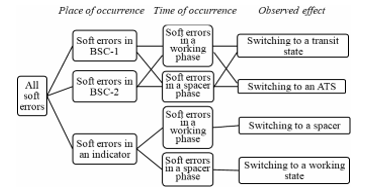 Figure 4 – Classification of the soft errors in the ST RS-flip-flops
4. Soft error cases in combinational ST circuits
According to the classification of soft errors given in Section 3 in Figure 1, the following types of soft errors are possible in a combinational ST circuit:
4.1. Switching DRS from VWS to an AS in a working phase;
4.2. Switching DRS from VWS to a spacer in a working phase;
4.3. Switching DRS from a spacer to an AS in a working phase;
4.4. Switching DRS from a spacer to a working state in a working phase;
4.5. Switching DRS from VWS to an AS in a spacer phase;
4.6. Switching DRS from VWS to a spacer in a spacer phase;
4.7. Switching DRS from a spacer to an AS in a spacer phase;
4.8. Switching the DRS from a spacer to a working state in a spacer phase.
Let’s assume that any of the situations 4.1 – 4.8 may appear because of a single bug with a probability of 1/8. Let’s estimate the likelihood of these soft errors corrupt data processed in the ST circuit. Corrupting data is precisely the critical situation. In other cases, a bug only leads to an additional delay in the ST circuit operation.
Case 4.1. ST circuits consider AS is a working state. Therefore, AS does not prevent the indication output of this ST circuit from switching to the working value and thereby initiating turning this ST circuit to the spacer phase. But AS actually contains a corrupted information bit. This ST circuit functioning logic does not mask AS with a probability of P4.1.1 = 0.5. AS appears at its output and then passes to the following ST circuits inputs. In the first approximation, we assume that, with a probability of P4.1.2 = 0.5, AS at the inputs of subsequent circuits corrupts their information outputs and leads to a critical error. Then the likelihood that situation 4.1 corrupts data equals to:
P4.1 = P4.1.1 × P4.1.2 = 0.25.
Case 4.2. Switching DRS from VWS to a spacer in a working phase means that the DRS has already turned to the VWS, but a bug caused it to switch back to the spacer. The ST circuit indication output can already acknowledge switching DRS into VWS. Since the indication subcircuit consists of triggers (i.e., C-elements or H-triggers), the indication output does not return to the spacer. With some probability, the DRS spacer causes switching of one or more DRS outputs of this ST circuit into the spacer. Subsequent ST circuits cannot complete their switch to a working phase due to the spacer on their inputs. They expect the appearance of a working state on all their significant inputs and prohibit the switching of this ST circuit into the spacer. This situation is not critical.
Case 4.3. This case means that a bug forces turning DRS to the AS instead of VWS. Similar to situation 4.1, the probability that situation 4.3 becomes critical equals P4.3 = 0.25.
Case 4.4. Switching DRS from a spacer to a working state in a working phase means that a bug caused a premature DRS transition to the working state. If this working state matches the expected VWS, the situation is not critical. However, with a probability of P4.4.1 = 0.5, this working state is IWS. As we noted earlier, the bug cannot affect both parts of DRS in opposite directions. Therefore, in this situation, a soft error appears on only one DRS part. Then the second DRS part switches to a working value under the influence of the working state of ST circuit inputs. As a result, a fail DRS turns to AS. Similar to situation 4.1, the probability that situation 4.4 becomes critical equals
P4.4 = P4.4.1 × P4.1 = 0.125.
Case 4.5. The ST circuit has already completed the switch to a working phase. With a probability of P4.5.1 = 0.5, the functional logic of this ST circuit does not mask AS. AS appears at the output of this ST circuit, and then passes to the following ST circuit inputs. With a probability of P4.5.2 = 0.5, the ST circuit output receivers have not yet switched to a working state, and AS takes part in the generation of their outputs. Then the probability that situation 4.5 becomes critical equals to:
P4.5 = P4.5.1 × P4.5.2 × P4.1 = 0. 0625.
Case 4.6. The ST circuit already completely switched to a working phase, and this soft error means a premature spacer. With some probability, the functional logic of this ST circuit does not mask the premature spacer. It appears at the output of this ST circuit. If these output receivers have not yet switched to a working state, a premature spacer can lock this switching. ST receivers suspend their work in anticipation of a working state on the failed inputs. They do not allow the inputs of this ST circuit in which a soft error occurred to switch to a spacer. This situation is not critical.
Case 4.7. The ST circuit has completed switching to a working phase, and DRS in which the soft error occurred has already turned to a spacer. The ST circuit output receivers also completed the switch to a working phase. AS can pause the switching this ST circuit to a spacer for the bug duration but is not critical.
Case 4.8. The ST circuit and its output receivers completed switching to the working phase, and DRS, in which the soft error occurred, has already turned to a spacer. The working state is premature. It can pause the switching this ST circuit to a spacer for the bug duration but is not critical.
Thus, only the soft errors in cases 4.1, 4.3, 4.4, and 4.5 are critical for the combinational ST circuit operation. The total probability of corrupting data processed in the ST circuits, because of soft errors classified in Section 3, equals to:
P4 = (1/8) × (P4.1 + P4.3 + P4.4 + P4.5) = 0. 0859375 ≈ 8.6%.
The soft errors that appeared in the indication subcircuit of the ST circuits are not critical. They can only cause an additional delay in the switching circuit from one phase to another.
5. Soft error cases in RSFFs
According to the classification of soft errors in the RSFFs in Figure 4, the following their types are possible:
5.1. Switching BSC-1 to a transit state in a working phase;
5.2. Switching BSC-1 to an ATS in a working phase;
5.3. Switching BSC-1 to a transit state in a spacer phase;
5.4. Switching BSC-1 to an ATS in a spacer phase;
5.5. Switching BSC-2 to a transit state in a working phase;
5.6. Switching BSC-2 to an ATS in a working phase;
5.7. Switching BSC-2 to a transit state in a spacer phase;
5.8. Switching BSC-2 to an ATS in a spacer phase;
5.9. Switching indicator to a spacer in a working phase;
5.10. Switching indicator to a working state in a spacer phase.
Let’s assume that any of the cases 5.1 – 5.10 may appear because of a single bug with a probability of 1/10. Let’s estimate the likelihood that these soft errors become critical and corrupt processed data.
Case 5.1. In a working phase of the ST RS-flip-flop, Rst = 0, R = S = 1. Suppose that before the soft error, the state of BSC-1 was (U = 0, UB = 1). The BSC-1 can switch to a transit state in the RSFF working phase in two situations:
5.1.1 Bug affects a logical level of a single BSC-1 output.
5.1.2. The bug affects the logical levels of both BSC-1 outputs.
In situation 5.1.1, the transit state of BSC-1 (U = UB = 1) turns to IWS (U = 1, UB = 0) as the bug affects only the output U of BSC-1. As a result, BSC-1 stores IWS. The spacer R = S = 1 causes an immediate rewriting of this IWS to BSC-2 and corrupts an information bit stored in the RSFF and presented at its output. Data corruption, not only in the RSFF but also in the subsequent data processing path, occurs in the following cases:
– With a probability of P5.1.1.1 = 0.5, the input {R, S} remains in the spacer until switching BSC-1 into IWS and writing IWS to BSC-2. With a likelihood of P5.1.1.2 = 0.5, IWS at the output {Q, QB} corrupts the data in the RSFF output receivers,
– With a probability of P5.1.1.3 = 0.5, the input {R, S} has time to switch to a new VWS before writing IWS from BSC-1 to BSC-2. Still, the new VWS with a probability of P5.1.1.4 = 0.5 is opposite to the IWS stored in BSC-1 and does not prevent writing IWS to BSC-2. In this case, BSC-1 returns to the transit state and supports the indicator working value. With a probability of P5.1.1.5 = 0.5, IWS at the output {Q, QB} corrupts the data in the RSFF output receivers.
In situation 5.1.2, the bug does not allow BSC-1 to switch from the transit state to the IWS. At R = S = 1, BSC-2 turns to its transit state (Q = QB = 0), which traditional ST circuits consider as a spacer, and the RSFF remains in the working phase. There are two ways of situation evolution:
– With a probability of P5.1.2.1 = 0.5, the RSFF output receivers complete switching to a working phase, despite the transit state of the RSFF output. Together with the RSFF indicator, they initiate the DRS {R, S} transition to a new VWS. With a probability of P5.1.2.2 = 0.5, BSC-1 is still in transit state. Then the VWS at RSFF input is written to BSC-2 as IWS. Still, the RSFF indicator remains in a working value and suspends the ST circuit operation until the bug ends. When bug ends, BSC-1 turns to VWS and toggles the RSFF indicator to a spacer. IWS in BSC-2 does not prevent the ST circuit from completing a transition to a spacer and initiating the switching of the RSFF input {R, S} to a spacer (R = S = 1), which rewrites VWS from BSC-1 to BSC-2. ST circuit continues operation with correct data;
– With a probability of P5.1.2.3 = 0.5, the RSFF output receivers do not complete switching to a working phase because of the RSFF output transit state. The ST circuit pauses while waiting for the RSFF working state. The DRS {R, S} remains in a spacer. At the bug end, the BSC-1 state becomes metastable. With a probability of P5.1.2.4 = 0.5, BSC-1 switches to IWS. The spacer R = S = 1 causes an immediate rewriting IWS to BSC-2. ST circuit continues to work with corrupted data.
The total data corruption probability in case 5.1 equals to:
P5.1 = 0.5×(P5.1.1.1 × P5.1.1.2 + P5.1.1.3 × P5.1.1.4 × P5.1.1.5) +
+ 0.5×(P5.1.2.3 × P5.1.2.4) = 0.3125.
Case 5.2. BSC-1 can switch to ATS (U = UB = 0) in an RSFF working phase also in two situations:
5.2.1 The bug affects a logical level of a single BSC-1 output.
5.2.2. The bug affects the logical levels of both BSC-1 outputs.
Suppose that before the bug, the state of BSC-1 was (U = 0, UB = 1). ATS in BSC-1 appears due to a failed switching UB from the logical 1 level to logical 0 level. In a working phase of ST RS-flip-flop, Rst = 0, R = S = 1, and BSC-2 stores VWS. ATS in BSC-1 does not damage the BSC-2 state, but ATS is not stable.
In situation 5.2.1, at the spacer R = S = 1, BSC-1 turns to IWS (U = 1, UB = 0), that is written to BSC-2, corrupting the data in the RSFF output receivers with a probability of P5.2.1.1 = 0.5.
In situation 5.2.2, at the spacer R = S = 1, BSC-1 remains in ATS until the bug end. With a probability of P5.2.2.1 = 0.5, the RSFF output receivers do not have time to switch into a working phase. So, they do not allow DRS {R, S} source to turn the RSFF inputs into a new VWS before the bug ends. At the bug end, BSC-1 is in a metastable state. With a probability of P5.2.2.2 = 0.5, it turns to a working state opposite to BSC-2 state, which is written to BSC-2, corrupting the data in the RSFF output receivers with a probability of P5.2.2.3 = 0.5.
The data corruption probability in case 5.2 equals to:
P5.2 = 0.5×P5.2.1.1 + 0.5×(P5.2.2.1 × P5.2.2.2 × P5.2.2.3) = 0.3125.
Case 5.3. BSC-1 can switch to a transit state (U = UB = 1) in an RSFF spacer phase in two situations:
5.3.1. The bug affects a logical level of a single BSC-1 output.
5.3.2. The bug affects the logical levels of both BSC-1 outputs.
In situation 5.3.1, BSC-1 may switch from the transit state to IWS. Let, for example, R = Rst = 0, S = 1, U = 0, UB = 1. BSC-1 output U switches to U = 1 because of the bug. With a probability of P5.3.1.1 = 0.5, the RSFF and its output receivers have already completed the transition to a spacer and initiated switching DRS {R, S} to a spacer. BSC-1 remains in transit state until input R switches to a spacer value (R = 1). With a probability of P5.3.1.2 = 0.5, the bug does not end by this time, and BSC-1 switches from the transit state to IWS (U = 1, UB = 0). IWS is written from BSC-1 to BSC-2 since R = S = 1 and appears at the RSFF output. With a probability of P5.3.1.3 = 0.5, IWS corrupts the data in the RSFF output receivers.
In situation 5.3.2, BSC-1 may also switch from transit state to IWS. Let, for example, R = Rst = 0, S = 1, U = 0, UB = 1. The bug switches BSC-1 output U to U = 1 and reinforces UB=1 value. With a probability of P5.3.2.1 = 0.5, the RSFF and its output receivers have already completed the transition to a spacer and initiated switching DRS {R, S} to a spacer. The BSC-1 remains in transit state until input R switches to the spacer value (R = 1). With a probability of P5.3.2.2 = 0.5, the bug does not end by this time, but BSC-1 cannot switch from the transit state to any working state because the bug forces the logical 1 level at both BSC-1 outputs. As a result, upon bug completion, BSC-1 is in a metastable state. With a probability of P5.3.2.3 = 0.5, it switches to the working state opposite to that of BSC-2. BSC-2 turns into this state. With a probability of P5.3.2.4 = 0.5, it corrupts data in the RSFF output receivers.
The total data corruption probability in case 5.3 equals to:
P5.3 = 0.5×(P5.3.1.1 × P5.3.1.2 × P5.3.1.3) +
+ 0.5×(P5.3.2.1 × P5.3.2.2 × P5.3.2.3 × P5.3.2.4) = 0.09375.
Case 5.4. BSC-1 can switch to ATS (U = UB = 0) in the RSFF spacer phase also in two situations:
5.4.1. The bug affects a logical level of a single BSC-1 output.
5.4.2. The bug affects the logical levels of both BSC-1 outputs.
In situation 5.4.1, BSC-1 switches from ATS to IWS. Let, for example, R = Rst = 0, S = 1, U = 0, UB = 1 before the bug. The output UB of BSC-1 switches to UB = 0 because of the bug. Since the bug did not affect the U node, condition UB = Rst = 0 causes switching U from logical 0 to logical 1 level, and BSC-1 turns to IWS (U = 1, UB = 0). The following writing IWS to BSC-2 turns indicator to a working value I = 0. Two directions of further evolution are possible:
– With a probability of P5.4.1.1 = 0.5, the RSFF and its output receivers have already completed the transition to a spacer and initiated switching DRS {R, S} to a spacer. With a probability of P5.4.1.2 = 0.5, BSC-1 remains in the IWS until the input R switches to a spacer value (R = 1). The RSFF input spacer writes the IWS from BSC-1 to BSC-2, which with a probability of P5.4.1.3 = 0.5 corrupts data in the RSFF output receivers;
– With a probability of P5.4.1.3 = 0.5, the RSFF and its output receivers do not have time to switch to a spacer. Input {R, S} remains in VWS until the bug end. At the bug end, BSC-1 switches to VWS, the RSFF indicator acknowledges the RSFF spacer state, and the ST circuit continues operation with the correct data.
In the situation, 5.4.2 BSC-1 can also switch from ATS to IWS. Let, for example, R = Rst = 0, S = 1, U = 0, UB = 1 before the bug. Bug switches the output UB of BSC-1 to UB = 0 and reinforce the value U = 0. BSC-1 remains in ATS and provides storage of VWS in BSC-2. The indicator acknowledges the RSFF spacer state. With a probability of P5.4.2.1 = 0.5, the RSFF output receivers complete the transition to a spacer and initiate switching DRS {R, S} to a spacer. With a probability of P5.4.2.2 = 0.5, BSC-1 remains in ATS until the input R switches to a spacer value (R = 1). Until the bug end, BSC-1 cannot switch from ATS to any working state, because the bug holds logical 0 levels at both outputs of BSC-1. At the bug end, BSC-1 enters a metastable state, which with a probability of P5.4.2.3 = 0.5, switches into the working state opposite to the initial VWS of DRS input {R, S}. BSC-2 turns to this IWS, and with a probability of P5.4.2.4 = 0.5, corrupts data in the RSFF output receivers.
The total data corruption probability in case 5.4 equals to:
P5.4 = 0.5×(P5.4.1.1 × P5.4.1.2 × P5.4.1.3) +
+ 0.5×(P5.4.2.1 × P5.4.2.2 × P5.4.2.3 × P5.4.2.4) = 0.09375.
Case 5.5. In a working phase of an RSFF, Rst = 0, R = S = 1. Suppose that before a bug, the states of the BSCs were (U = 0, UB = 1), and (Q = 1, QB = 0). BSC-2 can switch to a transit state in the RSFF working phase in two situations:
5.5.1. The bug affects a logical level of a single BSC-2 output.
5.5.2. The bug affects the logical levels of both BSC-2 outputs.
In situation 5.5.1, the transit state of BSC-2 (Q = QB = 0) switches the RSFF indicator to a spacer. Further situation evolution is possible in two directions:
– With a probability of P5.5.1.1 = 0.5, the RSFF output receivers complete switching into a working phase and initiate the transition of DRS {R, S} to a new VWS. A spacer value of the RSFF indicator remains until the bug ends. If a new VWS appears before the bug end, it supports the spacer value of the RSFF indicator, and the ST circuit continues regular operation. If the bug ends before the new input VWS, a condition R = S = 1 causes writing VWS from BSC-1 to BSC-2. It does not corrupt data in the RSFF output receivers;
– With a probability of P5.5.1.2 = 0.5, the RSFF output receivers do not complete switching into a working phase and do not initiate the transition of DRS {R, S} to a new VWS. The receivers consider the RSFF output transit state as a spacer. ST circuit pauses with its operation. At the bug end, the spacer R = S = 1 forces writing VWS from BSC-1 to BSC-2. BSC-2 restores its VWS, and the ST circuit continues regular operation with correct data.
Situation 5.5.2 is similar to the situation 5.5.1 and also cannot cause any data corruption. So, the total data corruption probability in case 5.5 equals P5.5 = 0.
Case 5.6. Let Rst = 0, R = S = 1, U = 0, UB = 1, Q = 1, QB = 0 in the ST RS-flip-flop working phase. BSC-2 can switch to ATS in two situations:
5.6.1. The bug affects only a logical level of QB output.
5.6.2. The bug affects the logical levels of both BSC-2 outputs.
In situation 5.6.1, ATS (Q = QB = 1) in BSC-2 forces switching BSC-2 to IWS (Q = 0, QB = 1) due to cross-connections. The RSFF indicator turns to a spacer value I = 1 and prevents the RSFF output receivers from using the {Q, QB} state.
With a probability of P5.6.1.1 = 0.5, the RSFF output receivers do not complete the switch to a working phase. They do not allow the RSFF input {R, S} source to initiate the transition of DRS {R, S} to a new VWS. At the bug end, the spacer R = S = 1 forces writing VWS from BSC-1 to BSC-2. BSC-2 restores its VWS, the RSFF indicator switches to a working value, and the ST circuit continues regular operation with correct data.
With a probability of P5.6.1.2 = 0.5, the RSFF output receivers have time to complete the switching to a working phase and allow the RSFF input {R, S} source to initiate the transition of DRS {R, S} to a new VWS. With a probability of P5.6.1.3 = 0.5, IWS at the output {Q, QB} during the switching RSFF indicator from a working value to a spacer has time to corrupt data in subsequent ST circuits. With a probability of P5.6.1.4 = 0.5, DRS {R, S} has time to switch to the new VWS before the bug ends. The RSFF indicator remains in the spacer and not allow for restoring corrupted data.
In situation 5.6.2, the ATS in BSC-2 (Q = QB = 1) does not switch into any working state, because of the bug forces logical 1 level on both BSC-2 outputs. The RSFF indicator remains in a working value I = 0 and allows the RSFF output receivers to use the {Q, QB} state. With a probability of P5.6.2.1 = 0.5, ATS at the output {Q, QB} corrupts data in the receivers of this output, since they consider it is a working state. With a probability of P5.6.2.2 = 0.5, the RSFF output receivers complete switching to a working phase. They initiate the transition of DRS {R, S} to a new VWS, which occurs, with a probability of P5.6.2.3 = 0.5, before the bug ends. The RSFF indicator switches to a spacer I = 1 and prohibits restoring corrupted data.
The total data corruption probability in case 5.6 equals to:
P5.6 = 0.5×( P5.6.1.2 × P5.6.1.3 × P5.6.1.4) +
+ 0.5×( P5.6.2.1 × P5.6.2.2 × P5.6.2.3) = 0.125.
Case 5.7. Let’s suppose that in the ST RS-flip-flop spacer phase, Rst = 0, R = 1, S = 0, U = 1, UB = 0, and before the bug, BSC-2 state was (Q = 0, QB = 1). In a spacer phase, the BSC-1 static state and the RSFF inputs do not affect the BSC-2 state. BSC-2 can switch to the transit state (Q = QB = 0) in the RSFF spacer phase in two situations:
5.7.1. The bug affects only a logical level of QB output.
5.7.2. The bug affects the logical levels of both BSC-2 outputs.
In situation 5.7.1, the transit state of BSC-2 (Q = QB = 0) turns to IWS (Q = 1, QB = 0) due to cross-connections, since the bug does not affect the logical level of Q. But the indicator remains in a spacer, and following the handshake discipline, the RSFF output receivers do not use IWS at the output of this RSFF. The RSFF indicator and its output receivers initiate the transition of DRS {R, S} to a spacer.
With a probability of P5.7.1.1 = 0.5, VWS in BSC-1 does not correspond to the BSC-2 state, as in the case under consideration. Since bug only affects QB, the condition (S = U = 1) causes switching output Q to Q = 0. BSC-2 turns back to the transit state considered as a spacer by subsequent ST circuits. The indicator remains in a spacer value I = 1. The RSFF output receivers do not complete switching to a working phase and do not allow the RSFF input {R, S} source to initiate the transition of DRS {R, S} to a new VWS. At the bug end, the QB output switches to QB = 1, and BSC-2 turns to the expected VWS. The ST circuit continues regular operation with correct data.
If the states of BSC-1 and BSC-2 coincide, then after the DRS {R, S} transition to a spacer, the ST circuit continues regular operation with uncorrupted data.
In situation 5.7.2, the transit state of BSC-2 (Q = QB = 0) does not switch into a working state, since the bug forces the logical level of both RSFF outputs. But the indicator also remains in a spacer. Following the handshake discipline, the RSFF output receivers switch to a spacer. Together with the RSFF indicator, they initiate the transition of DRS {R, S} to the spacer. Upon bug completion and switching DRS {R, S} to the spacer, BSC-2 turns to the state of BSC-1, and the ST circuit continues regular operation with correct data.
The total data corruption probability in case 5.7 equals to P5.7 = 0.
Case 5.8. Let’s suppose that in the ST RS-flip-flop spacer phase, Rst = 0, R = 1, S = 0, U = 1, UB = 0, and BSC-2 state is (Q = 0, QB = 1) before the bug. BSC-2 can switch to ATS in two situations:
5.8.1. The bug affects only a logical level of Q output.
5.8.2. The bug affects the logical levels of both BSC-2 outputs.
In situation 5.8.1, ATS in BSC-2 (Q = QB = 1) causes switching BSC-2 into IWS (Q = 1, QB = 0) due to cross-connections. The indicator is in a spacer value I = 1 regardless of the BSC-2 state. It prevents the RSFF output receivers from using the state {Q, QB}. The RSFF output receivers complete switching to a spacer and allow the RSFF input {R, S} source to initiate the transition of DRS {R, S} to a spacer.
With a probability of P5.8.1.1 = 0.5, DRS {R, S} has time to switch to the spacer (R = S = 1) before the bug ends. With a probability of P5.8.1.2 = 0.5, VWS in BSC-1 does not correspond to the BSC-2 state, as in the case under consideration. Since the bug forces logical 1 level at the output Q, condition (S = U = 1) cannot switch the output Q to Q = 0. BSC-2 remains in IWS, but the RSFF indicator does not turn to a working value I = 0. It does not allow the RSFF output receivers to use the {Q, QB} state before the bug ends, and BSC-2 turns into VSC stored in BSC-1. Only then the RSFF indicator switches to a working value I = 0 and allow the RSFF output receivers to use the state {Q, QB}. The ST circuit continues regular operation with correct data. If, after switching DRS {R, S} to the spacer, the VWS in BSC-1 coincides BSC-2 state, the ST circuit also continues to work with the correct data.
With a probability of P5.8.1.3 = 0.5, DRS {R, S} does not have time to switch to the spacer (R = S = 1) before the bug ends. The input {R, S} working state, and VWS in BSC-1 prevent writing to the BSC-2. At the bug end, BSC-2 continues to store IWS. Still, due to the spacer value of the RSFF indicator, the RSFF output receivers do not use it, and their data remains uncorrupted.
In situation 5.8.2, ATS in BSC-2 (Q = QB = 1) does not cause the BSC-2 to switch into any working state, because of the bug forces logical 1 level on both outputs of BSC-2. The RSFF indicator remains in a spacer value I = 1 and prevents the RSFF output receivers from using ATS. The RSFF output receivers complete switching to the spacer and allow the RSFF input {R, S} source to initiate the transition of DRS {R, S} to a spacer.
With a probability of P5.8.2.1 = 0.5, DRS {R, S} has time to switch to the spacer (R = S = 1) before the bug ends. Because of ongoing bug, BSC-2 does not turn into VWS stored in BSC-1. ATS at the output {Q, QB} causes switching the RSFF indicator to a working value I = 0, which allows the RSFF output receivers to use the ATS as a working state. With a probability of P5.8.2.2 = 0.5, the ATS corrupts data in the RSFF output receivers.
With a probability of P5.8.2.3 = 0.5, DRS {R, S} does not have time to switch to the spacer (R = S = 1) before the bug ends. The input {R, S} working state, and VWS in BSC-1 prevent writing to BSC-2. After the bug ends, BSC-2 is in a metastable state, which switches to an arbitrary working state. But due to the spacer value of the RSFF indicator, the output {Q, QB} working state is not used by the RSFF output receivers, and their data remains uncorrupted.
The total data corruption probability in case 5.8 equals to:
P5.8 = 0.5×( P5.8.2.1 × P5.8.2.2) = 0.125.
Case 5.9. It suggests the indicator has switched to the working value but returned to the spacer because of the bug. In this case, BSC-1 and BSC-2 store VWS. Since the data inside and at the RSFF information output do not change, a failed switching indicator to the spacer, in the worst case, only pauses the ST circuit regular operation. When the bug ends, the RSFF indicator returns to the working value, and the ST circuit continues the correct operation.
The total data corruption probability in case 5.9 equals to P5.9 = 0.
Case 5.10. It assumes the indicator has switched to the spacer but returned to the working state because of the bug. In this case, BSC-1 and BSC-2 store VWS. Similarly, to case 5.9, when the bug ends, the RSFF indicator returns to the spacer, and the ST circuit continues the correct operation.
The total data corruption probability in case 5.10 equals to P5.10 = 0.
The reasoning given above for the specific values of the inputs, outputs, and internal state of the ST RS-flip-flop in cases 5.1 – 5.8 is also valid for any other initial conditions.
Thus, only the soft errors in the ST RS-flip-flop in cases 5.1 – 5.4, 5.6, and 5.8 are critical for the ST circuit functioning. The total data corruption probability because of a single soft error in the ST RS-flip-flop equals to:
P5 = (1/10) × (P5.1 + P5.2 + P5.3 + P5.4 + P5.6 + P5.8) = 0.10625.
Failure analysis for other types of STSCs gives a similar result. We do not cite it due to the limited volume of the paper.
6. Masking critical failures in ST circuits
6.1 Masking soft errors in ST combinational circuits
The following two methods, being used simultaneously, can improve soft error tolerance of the ST circuit:
- masking AS state,
- improvements in the ST pipeline indication.
The first method uses the fail-safe DRS discipline, considering AS is the second spacer [1], as shown in Table 1. Two spacers inside the same circuit were used earlier in secure dual-rail logic [20] and NCL circuits [11]. There they were formed by the different DRS sources and provided increased security for data encoding [20] or reduced power consumption [11]. We propose to indicate the AS as a valid second spacer of the same DRS.
Table 1: Fail-safe DRS discipline in ST circuits
| S.No | Synchronous signal X | ST signal | State | |
| X | XB | |||
| 1 | 0 | 0 | 1 | bit 0 |
| 2 | 1 | 1 | 0 | bit 1 |
| 3 | – | 0 | 0 | spacer 0 |
| 4 | – | 1 | 1 | spacer 1 |
XNOR, or “equivalence” cell, indicates two DRS spacers (“00” and “11”). Figure 5 shows two XNOR implementations suitable for use in QDI circuits. The circuit in Figure 5(a) [21] is convenient for implementation with a standard cell library. The circuit in Fig. 1(b) has the least possible transistor number.
The two-phase discipline of the ST circuit operation and the requirement of a mandatory indication of each DRS mask a mixed spacer-working state at the circuit inputs. Indeed, the DRS consistently switches from spacer to a working state and back to spacer state. The indicator acknowledges the completion of this switching to each state. The indicator also acknowledges the incorrect switching DRS to a state that does not correspond to the ST circuit operation phase. As a result, the indicator does not correspond to an expected one in the current phase of the ST circuit. An indication subcircuit detects and localizes this case.
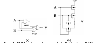 Figure 5 – XNOR implementation: on standard cells (a) and pass CMOS transistors (b)
Thus, the usage of a double spacer allows one to mask all soft errors causing the AS appearance in combinational ST circuits, namely, cases 4.1, 4.3, 4.4, and 4.5 in Section 4.
As a result, with the indication subcircuit slight complication providing AS indication as a spacer, the combinational ST circuits mask soft errors in all cases analyzed in Section 4. An improved method for controlling the phases of the output register during pipeline implementation of the ST circuit retains this advantage within the framework of the general ST circuit.
Figure 6 shows a circuit of an optimized ST pipeline utilized in the Fused Multiply-Add (FMA) project [22]. The logic and register parts implement the pipeline stage. LI* and RI* blocks compress the logical part and register bitwise indicators in each pipeline stage into one total indication signal, respectively. The output signals of the LI* and RI* blocks indicate the completion of the switching of all cells in the pipeline stage, “fired” by the stage inputs in the current operation phase.
 Figure 6 – Traditional ST pipeline
H-trigger [16] collects the outputs of the blocks LIk+1 and RIk+1, forming a control signal for the output register of the k-th pipeline stage within the ST pipeline handshake discipline. The k-th stage output register, in turn, forms the working state and the spacer of the logical part inputs of the (k+1)-th pipeline stage.
The H-trigger is a static analog of the Muller C-element [16], traditionally used for ST circuit indication. Figure 7 shows the two-input H-trigger CMOS circuit. Unlike the C-element, the H-trigger does not contain a “weak” inverter, and due to this, it has better noise immunity. Table 2 represents the truth table of the two-input H-trigger. If the states of the inputs I0 and I1 are equal, then output Q turns to the same state. Otherwise, output Q stores its state.
 Figure 7 – CMOS circuit of the two-input H-trigger
Table 2: Truth table of the two-input H-trigger
| S.No | Inputs | Output, Q+ | |
| I0 | I1 | ||
| 1 | 0 | 0 | 0 |
| 2 | 1 | 0 | Q |
| 3 | 0 | 1 | Q |
| 4 | 1 | 1 | 1 |
Note that the pipeline control circuit in Figure 6 is correct only if the logic block of the current pipeline stage indicates all previous pipeline stage register outputs. Otherwise, the H-trigger controlling the k-th stage register must have a third input connected to this register indication output.
Figure 8(a) shows a one register bit implementation, where the DRS inputs {Xj, XBj} have a unit spacer. It consists of two H-triggers. Due to this, it stores both the working and spacer states of DRS inputs {Xj, XBj}, while ensuring an indication of all its inputs and outputs. Ph input is a total phase control signal for all register bits. When the k-th pipeline stage combinational part switches to a spacer phase, its output register, for some time, is in the working phase and provides the k-th stage outputs to the (k+1)-th stage inputs.
 Figure 8 – ST register bit: traditional (a) and soft error resisted (b)
The indicators of the combinational part and the register of the (k+1)-th stage acknowledge their switching to the working phase. Then the H-trigger combining them forms the spacer value of the general register control signal Ph. Only after this, the register becomes insensitive to the working state changes of the inputs {Xj, XBj}. Therefore, for some time, any working state change at the output of the k-th stage combinational part is stored in its output register and transferred to the (k+1)-th pipeline stage inputs.
The register bit circuit complication, as shown in Figure 8 (b), increases its tolerance to soft errors. Then register indicates the AS state of the {Yj, YBj} output as a spacer.
Table 3 displays the data corruption probabilities for the cases discussed in Section 4 in the classical combinational ST circuit and the ST circuit using the proposed circuit techniques increasing soft error tolerance. The last row shows the total data corruption probability in combinational ST circuits because of soft errors analyzed in Section 4, taking into account the equal likelihood of their occurrence.
Table 3: Data corruption probabilities in classical and
improved combinational ST circuit
| Soft error case |
Classical ST circuit |
Improved ST circuit |
| 4.1 | 0.25 | 0 |
| 4.2 | 0 | 0 |
| 4.3 | 0.25 | 0 |
| 4.4 | 0.125 | 0 |
| 4.5 | 0.125 | 0 |
| 4.6 | 0 | 0 |
| 4.7 | 0 | 0 |
| 4.8 | 0 | 0 |
| Total | 8.6% | 0% |
Thus, classical ST combinational circuits mask soft errors classified in Section 3 in 91.4% of their occurrence cases. AS indication as a spacer and the bit implementation of the pipeline stage output register by the circuit in Figure 8(b) mask the remaining 8.6% of soft error cases in the combinational ST circuit that are not masked by the classical ST circuits properties and their interaction discipline.
Remind, we consider the soft errors that occur too close to the ST circuit current phase end or having a too long duration. So, the ST circuit two-phase discipline cannot mask them. In synchronous circuits, critical soft errors having no time to disappear before the active clock edge arrives. They can only be masked by using fail-safe coding or through special circuitry techniques that increase the hardware complexity.
6.2 Masking soft errors in STSCs
The usage of ST RSFFs with DRS information outputs [19] and circuitry methods improving the failure-tolerance of memory circuits (for example, LTMR [23], DICE [24, Figure 3]) allow for essential increasing the STSC soft error tolerance.
Combinational ST circuits use DRS inputs, while the RSFF information outputs in Figure 3 form a signal without spacer. The RSFF with DRS information input {R, S} and output {QP, QPB}, shown in Figure 9, resolves this problem.
The RSFFs with DRS information output write the BSC-2 state to their information outputs only in the working phase of the BSC-2 and only when its state corresponds to the BSC-1 state. The inputs of the RSFF shown in Figure 9 have a unit spacer (R = S = 1), which forces writing BSC-1 state to BSC-2. Indicator value I = 0 acknowledges this write successful completion and allows for switching DRS outputs (QP, QPB) to a working state corresponding to the BSC-2 state. The working state at the RSFF information inputs ({R = 0, S = 1} or {R = 1, S = 0}) causes switching the RSFF indication output to I = 1 and forces turning DRS output to the spacer (QP = QPB = 0). Therefore, any change in the BSC-2 state in this phase does not affect the RSFF output state.
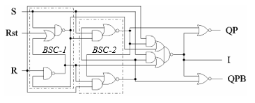 Figure 9 – ST RS-flip-flop with DRS input and output
The indication output spacer value I = 1 or ATS in BSC-2 force the spacer at the {QP, QPB} output of the RSFF in Figure 9. As a result, the data corruption probabilities P5.6.2.1 and P5.8.2.2 for ATS at {QP, QPB} output become zero. Then the probabilities of cases 5.6 and 5.8 from Section 5 become equal to P5.6 = 0.0625 and P5.8 = 0, and the total data corruption likelihood because of the soft error in the RSFF shown in Figure 9 decreases to P5 = 0.0875 ≈ 8.8%.
DICE (Dual Interlocked Cell) is a particular circuitry method for protecting RAM cells and a sequential logic against soft errors. First, it doubles hardware, using cross-connections to control the gates of p- and n-type transistors in the symmetric parts of the circuit. Second, it assumes spacing the corresponding layout fragments to avoid a simultaneous impact on them the same particle. Figure 10 shows an example of a dice-style synchronous D-latch [24, Figure 3].
 Figure 10 – Synchronous DICE-style D-latch
LTMR (Localized Triple Modular Redundancy) is a method of local majoring applied at the level of individual logical cells. Figure 11 demonstrates an example of a synchronous LTMR flip-flop [23].
The LTMR method surpasses the DICE approach in protecting high-performance synchronous circuits against single failures. It masks failure in the assumption that the failure occurs only in one of the three parts of the circuit and does not corrupt the result of data processing. Unlike LTMR, DICE prevents writing incorrect state to the sequential cell and provides a self-healing of the circuit after the end of the failure. But writing the correct state to the sequential cell requires a time exceeding the duration of the failure. Therefore, the effectiveness of the DICE method drops, as the clock frequency increases.
The DICE method has lower hardware complexity comparing to LTMR one. So, it is preferable for use in the failure-resisted STSCs since they are inherently more complex than synchronous counterparts because of the dual-rail discipline and obligatory indication. In STSCs, LTMR method usage leads to a manifold complexity increase not only in the STSC’s functional part but also in its indication subcircuit. As a result, not only the time parameters and energy consumption deteriorate, but also the reliability characteristics (for example, the average time between failures).
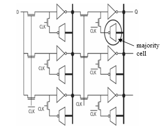 Figure 11 – Synchronous LTMR flip-flop
STSCs specificity makes it easy enough to adapt the DICE method for increasing their soft error tolerance. Figure 12(a) represents the synchronous simplified RS-latch circuit on NAND2 cells, which implements a DICE-like approach. The NAND2 cells are spaced a sufficient distance in a layout to minimize the probability of several particles impact them simultaneously.
Figure 12(b) shows a real DICE-style RS-latch circuit implementation [25]. Signals in the pairs {S1, S2}, and {R1, R2} are logically equivalent and correspond to the S and R inputs in Figure 12(a). They are also spaced in the layout, as the increase in parasitic capacitance between them contributes to a growth in the sequential cell failure-tolerance [25]. Figure 12(b) demonstrates the real connections of the internal nodes of the circuit with the gates of transistors. Such the circuit successfully resists against the effects of a single particle in any submicron CMOS process.
However, an analysis shows that a significant difference in the time of switching its homogeneous inputs into the active state leads to the short-circuit current in the RS-latch. Let, for example, the RS-latch state in Figure 12(b) is R1=R2=S1=S2=1, Q1=Q2=1, QB1=QB2=0, and (R1, R2) inputs switch to logic-zero state (R1®0, R2®0), R2 input does this later than R1. Switching R1®0 results in unlocking the transistor P5, turning the node QB1®1, and unlocking the transistor N1. Since transistor N3 is already open (S2=1), node QB1 connects to the power supply through transistor P2 and to the ground through a chain of open transistors N1 and N3. Short-circuit current flows between the power and ground buses. It stops only after switching R2®0 and charging QB2 node to a high potential, sufficient to close P2 transistor. Therefore, the R1 and R2, S1, and S2 nets should be paired with symmetry when implementing the RS-latch layout, so that the signal propagation delays along them are not too different.
 Figure 12 – DICE-style RS-latch: schematic view (a) and CMOS circuit (b)
Using the DICE-like approach to implement STSCs also improves their failure-tolerance while complying with specific layout design rules. BSC built on the DICE-style RS-latch (Figure 12(a)) has two times more outputs than a conventional BSC. The DICE approach leads to doubling an STSC functional part. The principles of the ST circuits require an indication of all STSC inputs and outputs. Therefore, an increase in the number of outputs of the functional part also complicates the indication subcircuit.
Figure 13 shows a conventional ST RS-latch circuit, which information input is the DRS with a unit spacer. At the same time, the OAI22 cell implements an indication subcircuit. Figure 14 demonstrates the DICE implementation of the same latch. The indication subcircuit is more complex, as it should indicate all outputs in the ST circuit, but does not double.
 Figure 13 – Conventional ST RS-latch
 Figure 14 – DICE-style ST RS-latch
Figures 3 and 15 demonstrate a similar conversion of the original RS-flip-flop. The conventional ST RS-flip-flop shown in Figure 3 has two BSCs. In contrast, the failure-resisted DICE implementation shown in Figure 15 has duplicated BSCs. The indicator of the DICE implementation also is complicated but not doubled.
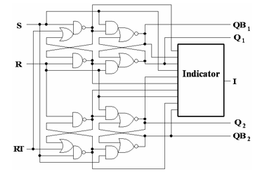 Figure 15 – DICE-style ST RSFF
Table 4: Data corruption probabilities in classical and advanced ST RSFF
| Soft error case |
Classical ST RSFF |
Advanced ST RSFF | |
| with DRS output | DICE-style | ||
| 5.1 | 0.3125 | 0.3125 | 0 |
| 5.2 | 0.3125 | 0.3125 | 0 |
| 5.3 | 0.09375 | 0.09375 | 0 |
| 5.4 | 0.09375 | 0.09375 | 0 |
| 5.5 | 0 | 0 | 0 |
| 5.6 | 0.125 | 0.0625 | 0 |
| 5.7 | 0 | 0 | 0 |
| 5.8 | 0.125 | 0 | 0 |
| 5.9 | 0 | 0 | 0 |
| 5.10 | 0 | 0 | 0 |
| Total | 10.6% | 8.8% | 0% |
Table 4 displays the data corruption probabilities in the ST circuit because of the soft errors, classified in Section 3 and analyzed in Section 5, for the ST RSFF implemented by the classical circuit (Figure 3), the circuit with DRS output (Figure 9), and DICE-style circuit. The last row shows the total data corruption probability because of soft errors in the RSFF discussed in Section 5, taking into account the equal probabilities of their occurrence.
Thus, STSCs, unlike synchronous standard sequential cells and memory cells, mask 89.4% of soft errors analyzed in Section 5 due to their properties. The use of the ST RS-flip-flops with a DRS information output increases the tolerance to the soft errors discussed in Section 5, up to 91.2%. As in synchronous circuits, the DICE-style technique makes STSCs insensitive to remaining critical failures.
7. Conclusions
Due to using dual-rail code with spacer, two-phase operation discipline, and mandatory indication, ST circuits mask most of the short-term soft errors without any changes in their circuitry. Classical ST circuit implementations guarantee the high level of masking soft faults classified in Section 3: 91.4% in combinational ST circuits and 89.4% in ST sequential circuits.
The indication of prohibited DRS state that is opposite to the spacer state, as the second spacer masks remained classified soft errors in the combinational ST circuits.
The increase of the ST sequential circuits tolerance to the soft errors analyzed in Section 5 up to 91.2% is achieved by using ST RS-flip-flops with a dual-rail information output. DICE-style approach for implementing ST sequential circuits provides an additional increase of their tolerance to discussed soft errors up to 100%.
Thanks to ST circuit ability to mask most of the soft errors due to their features and their ability to maintain functional performance in a wide range of operating conditions, ST circuits are a promising basis for designing failure-resisted digital hardware.
Conflict of Interest
The authors declare no conflict of interest.
Acknowledgment
We would like to acknowledge the help of Dr. Alexander Kushnerov in discussing and preparing the paper. The study was funded by a grant from the Russian Science Foundation (Project № 19-11-00334).
- Y. A. Stepchenkov, A. N. Kamenskih, Y. G. Diachenko, Y. V. Rogdestvenski, D. Y. Diachenko, “Fault-Tolerance of Self-Timed Circuits” in 2019 10th International Conference on Dependable Systems, Services, and Technologies (DESSERT), Leeds, United Kingdom, 2019. https://doi.org/10.1109/DESSERT.2019.8770047
- A. I. Chumakov, “Forecasting local radiation effects in IC under the influence of the outer space factors” Microelectronics, 39(2), 85-90, 2010 (article in Russian with an abstract in English)
- P. Eaton, J. Benedetto, D. Mavis, K. Avery, M. Sibley, M. Gadlage, T. Turflinger, “Single event transient pulse width measurements using a variable temporal latch technique” IEEE Trans. Nucl. Sci., 51(6), 3365–3368, 2004. https://doi.org/10.1109/TNS.2004.840020
- B. Wiseman, “Design and Testing of SEU/SEL Immune Memory and Logic Circuits in a Commercial CMOS Process” in IEEE Radiation Effects Data Workshop, 1994, 51-55. https://doi.org/10.1109/REDW.1994.633039
- S. I. Ol’chev, V. Y. Stenin, “CMOS logic elements with increased failure resistance to single-event upsets” Russian Microelectronics, 40(3), 156-169, 2011. https://doi.org/10.1134/S106373971103005X (article in Russian with an abstract in English)
- J. E. Knudsen, L. T. Clark, “An area and power-efficient radiation hardened by design flip-flop” IEEE Trans. on Nucl. Sci., 53(6), 3392-3399, 2006.https://doi.org/10.1109/TNS.2006.886199
- Y. Monnet, M. Renaudin, R. Leveugle, “Hardening techniques against transient faults for asynchronous circuits“ in 11th IEEE International Conference: On-Line Testing Symposium, IOLTS 2005. https://doi.org/10.1109/IOLTS.2005.30
- S. F. Tyurin, A. N. Kamenskih, “Research into the reservation of logic functions at transistor level” In a world of scientific discoveries, 10(58), 232-247, 2014. https://doi.org/10.12731/wsd-2014-10-18 (article in Russian with an abstract in English).
- C. LaFrieda, R. Manohar, “Fault Detection and Isolation Techniques for Quasi Delay-Insensitive Circuits” in International Conference on Dependable Systems and Networks, 2004. https://doi.org/10.1109/DSN.2004.1311875
- A. Balasubramanian, B. L. Bhuva, J. D. Black, L. W. Massengill, “RHBD techniques for mitigating effects of single-event hits using guard-gates” IEEE Trans. on Nucl. Sci., 52(6), 2531-2535, 2005. https://doi.org/10.1109/TNS.2005.860719
- M. T. Moreira, G. Trojan, F. G. Moraes, N. L. V. Calazans, “Spatially distributed dual-spacer null convention logic design” Journal of Low Power Electronics, 10(3), 313-320, 2014. https://doi.org/10.1166/jolpe.2014.1332
- S. A. Aketiy, S. G. H. Cheng, J. Mekiey, P. A. Beerel, “SERAD: Soft Error Resilient Asynchronous Design using a Bundled Data Protocol,” arXiv:2001.04039 [cs.AR]. http://https://arxiv.org/abs/2001.04039v1
- A. Taubin, A. Kondratyev, J. Cortadella, L. Lavagno, “Behavioral Transformations to Increase Noise Immunity in Asynchronous Specifications,” in International Symposium on Advanced Research in Asynchronous Circuits and Systems, 1999. https://doi.org/10.1109/ASYNC.1999.761521
- D. Muller, W. Bartky, “A theory of asynchronous circuits” Annals of computation laboratory of Harvard University, V.29, 204-243, 1959.
- K. M. Fant, S. A. Brandt, “NULL Convention Logic: a Complete and Consistent Logic for Asynchronous Digital Circuit Synthesis” in International Conference on Application-Specific Systems, Architectures, and Processors, 1996. https://doi.org/10.1109/ASAP.1996.542821
- M. Kishinevsky, A. Kondratyev, A. Taubin, V. Varshavsky, Concurrent Hardware: The Theory and Practice of Self-timed Design, J. Wiley, 1994.
- Y. A. Stepchenkov, Y. G. Diachenko, V. S. Petrukhin, A. V. Filin, “The price of realizing the unique properties of self-timed circuits” Systems and means of informatics, 9, 261-292, 1999. (article in Russian with an abstract in English)
- Y. A. Stepchenkov, Y. G. Diachenko, G. A. Gorelkin, “Self-Timed circuits are the Microelectronics Future” Radio-electronic issue, 2, 153-184, 2011 (article in Russian with an abstract in English).
- Ю. А. Степченков, А. Н. Денисов, Ю. Г. Дьяченко, Ф. И. Гринфельд, О.П. Филимоненко, Н. В. Морозов, Д. Ю. Степченков, Л. П. Плеханов,Библиотека функциональных ячеек для проектирования самосинхронных полузаказных БМК микросхем серий 5503/5507, Техносфера, 2017. ISBN 978-5-94836-332-5 (in Russian).
- D. Shang, A. Yakovlev, A. Koelmans, D. Sokolov, A. Bystrov, “Registers for Phase Difference Based Logic” IEEE Trans. Very Large Scale Integration (VLSI) Systems, 15(6), 720-724, 2007. https://doi.org/10.1109/TVLSI.2007.898772
- Y.-C. Rhee, “Exclusive-OR and/or Exclusive-NOR Circuits Including Output Switches and Related Methods,” US Patent No. 7,312,634 B2, 2007
- Y. Stepchenkov, Y. Rogdestvenski, Y. Diachenko, D. Stepchenkov, Y. Shikunov, “Energy Efficient Speed-Independent 64-bit Fused Multiply-Add Unit” in 2019 IEEE Conference of Russian Young Researchers in Electrical and Electronic Engineering (EIConRus2019), 2019. https://doi.org/10.1109/EIConRus.2019.8657207
- M. Berg, “Revisiting Dual Interlocked Storage Cell (DICE) Single Event Upset (SEU) Sensitivity” in Microelectronics Reliability & Qualification Work Meeting (MRQW) 2013 and HiREV Industry Day, El Segundo, CA, December 10-12, 2013.
- T. Lakshmivaraprasad, M. Sivakumar, B. K. V. Prasad, S. A. Inthiyaz, “Nanoscale CMOS technology for hardened latch with efficient design” International Journal of Electronics and Communication Engineering, 5(3), 343-349, 2012. ISSN 0974-2166
- Y. V. Katunin, V. Y. Stenin, P. V. Stepanov, “Simulation of trigger two-phase CMOS logic cell characteristics, taking into account the separation of charge at the effects of individual nuclear particles” Microelectronics, 43(2), 104-117, 2014. https://doi.org/10.7868/S0544126914020069 (article in Russian with an abstract in English)