Enabling 3D Heterogeneous Structures Towards Smart Chips: A Review

Adv. Sci. Technol. Eng. Syst. J. 5(1), 267–273 (2020);
 DOI: 10.25046/aj050134
This review paper discusses recent research outcomes of fabricating three-dimensional (3D) heterogeneous structures in complementary metal-oxide-semiconductor (CMOS) integrated circuit (IC) technologies to enable smart future chips. The CMOS-based 3D heterogeneous structures demonstrated are vertical magnetic-cored inductors for radio-frequency (RF) ICs, through-back-end-of-line (BEOL) metal wall structures for global flying noise isolation, above-IC nano crossbar array electrostatic discharge (ESD) protection devices and graphene-based nano electromechanical (NEM) switch ESD protection structures, and individually controlled multiple-gated MOS field-effect transistors (MOSFET) for non-binary computing. These disruptive 3D heterogeneous structure concepts can potentially enable future smart IC chips in Si CMOS IC platforms.
1. Background
Since the birth of silicon monolithic integrated circuits (ICs) in 1959, geometrical scaling has been driving advances in silicon IC technologies, keeping on increasing transistor count at the Moore’s Law pace until late 1990s [1]. The hallmark Si planar process was the technical foundation that has been guided by the National Technology Roadmap for Semiconductor (NTRS) through 1990s [2]. The laterally dimensional scaling has evolved into equivalent scaling, as guided by the International Technology Roadmap for Semiconductor (ITRS) until 2000 [3], where new materials and structural features, such as strained silicon and FinFET, were included. Later, 3D Power scaling kicked in to accommodate the ever-increasing demands for and emerging challenges of density, complexity and power as IC technologies continue to advance to sub-10nm nodes, as guided by ITRS 2.0 until 2015 [4]. Nevertheless, as 7nm CMOS is already in production today and 3nm CMOS is on the horizon, lateral shrinking is quickly approaching its end. Since the horizontal Si “land” is limited for increasingly complex ICs, going vertical to make Manhattan style Si-based “skyscrapers” becomes an obvious alternative. Meanwhile, future chips are not only bigger and more complicated, they ought to be smarter too, demanding for more device functionalities to handle more information diversity. Consequently, the ITRS 2.0 was brought to its end in 2015 [5] and the new Heterogeneous Integration Roadmap (HIR) was initiated to address the emerging technical needs and challenges in the new era of integrated circuits and systems [6-7]. The required functional diversification cannot not be delivered by conventional Si IC devices. Many novel devices and structures will be needed, which must be heterogeneously integrated into Si ICs in a 3D fashion, mainly based upon the CMOS platforms. To this end, substantial R&D efforts have been devoted to developing non-traditional 3D heterogeneous devices and structures to enhance functionality and improve performing characteristics of conventional Si-based CMOS ICs. For example, Nanoelectromechanical (NEM) relay structure in CMOS backend was recently reported to realize reconfigurable interconnects to enable complex and hard-reconfigurable ICs [8]. This review paper, an extended version of our paper presented at IEEE International Conference on IC Design and Technology [9], provides an overview of our recent research outcomes of developing various disruptive 3D heterogeneous structures to enable smart future CMOS chips.
2. Vertical Magnetic-Cored Inductors
Proliferation of wireless communications have changed our society and the foundation is RF IC technology. The ultimate design goal is to achieve RF system-on-a-chip (SoC) to ensure higher system performance and reliability while reducing costs. The main technical barrier for making RF SoCs is lack of super compact, multiple-GHz, high-performance IC inductors in CMOS. Traditional IC inductors using metal spirals are too large, typically bigger than a bonding pad, which makes single-chip RF SoC impractical. The dream for RF IC designers is to have high-performance transistor-sized inductors in CMOS. For years, various magnetic-enhanced inductor structures have been reported, utilizing lateral magnetic films or complex MEMS structures to reduce magnetic losses. These magnetic inductors are impractical to CMOS ICs. As a solution, we proposed a novel stacked-via vertical-magnetic-cored inductor structure made in the back-end-of-line (BEOL) of CMOS [10-17]. To understand our disruptive concept, imagine to shrink a perfect discrete solenoid inductor and plugged it vertically into the CMOS BEOL stack, like a “needle”, which forms a transistor-sized vertical-magnetic-cored inductor in CMOS BEOL stacks. As the inductor size shrinks, electrical loss increases due to increased series resistance of metal wires, which however, can be compensated by reducing magnetic loss by use of a closed-loop magnetic circuit. Hence, the overall inductor performance does not suffer from inductor shrinking. Figure 1 depicts the concept of the new vertical- magnetic-cored inductor. Taking full use of CMOS BEOL structures, the vertical magnetic bar can be fabricated by locally replacing the common metal vias in a CMOS BEOL stack with suitable magnetic materials, hence called a stacked-via magnetic-cored inductor. One critical specification for the magnetic-cored inductor is to achieve high performance (e.g., Q-factor and inductance density, L-density) at high frequencies (>1GHz). Substantial theoretical and experimental work has been conducted to prototype the new inductor devices and improve the inductor performance [10-19]. Various magnetic materials compositions, materials synthesis techniques, magnetic core structures and process steps were explored. In our initial work, ferrite thin film materials, e.g., Ni0.4Zn0.4Cu0.2Fe2O4, Y2.8Bi0.2Fe5O12 and Co7ZrO9, were used as the magnetic media. A CMOS-compatible process module was developed using a spin-coating method to make single-layer ferrite magnetic enhanced inductors. As depicted in Figure 2, measurements showed encouraging inductance improvement over the non-magnetic references (R1/R2), from 5.8% to 38% up to 9GHz. To enhance magnetic materials for multiple-GHz operations, we further engineered various nano particle powders for the magnetic cores, including Co2Z-type (Ba3Co2Fe24O41) and Ni–Zn–Cu (Ni1−x−yZnxCuyFe2O4) series. We found that the Ni–Zn–Cu (Ni1−x−yZnxCuyFe2O4) composites achieved the best reported performance up to ~10GHz. We then developed a post-CMOS process flow to fabricate the vertical magnetic cores for RF inductors as shown in Figure 3. The new vertical magnetic-cored inductors were fabricated in a foundry 180nm 6-metal CMOS technology. Shown in Figure 4, the new magnetic-cored inductors achieved the then- best-reported inductor performance, i.e., Qmax∙fmax~L-density characteristics: ~220% improvement in Q-factor to up to 20GHz and the highest reported L-density of ~700nH/mm2 at Qmaxfmax of ~4GHz. A new 3D modeling technique was developed to accurately simulate any arbitrary conductor-magnet structures to guide the design and optimization of vertical magnetic-cored inductors [18, 19]. The new stacked-via magnetic-cored structure can be used to fabricate other types of compact high-performance inductive devices, which may not only reduce RF IC chip size, but also potentially allow new chip architecture. For example, a bank of compact magnetic-cored transformers can be used to realize simplified power amplifier (PA) architecture to address the power back-off problem. The new magnetic-cored inductors were applied to design of LC-VCO ICs in CMOS [20, 21]. Figure 5 shows that in a 1.36–1.86GHz VCO fabricated in a 180nm RF CMOS, it achieves a high FOM factor of ~202dBc/Hz and a reduced phase noises of -121 dBc/Hz at 100-kHz [12]. In a 2.22-2.92GHz VCO fabricated in a 180nm SOI CMOS, it achieves phase noise reduction for from -106.97dBc/Hz to -113.49dBc/Hz [21].
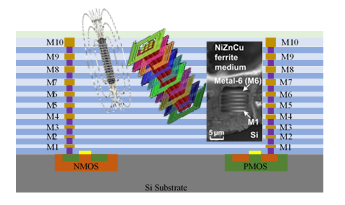 Figure 1 A conceptual view of new vertical magnetic cored inductor in CMOS platform. Insets from Left to Right: a discrete solenoid, simulated vertical magnetic-cored inductor and fabricated vertical magnetic-cored inductor.
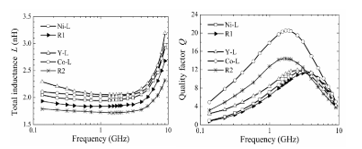 Figure 2 Measurement of initial single-layer magnetic-enhanced inductor shows improvement in inductance and Q-factor: Ni-L versus R1 and Y-L/Co-L versus R2 [10].
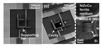 Figure 3 SEM photos for samples of fabricated vertical magnetic-cored inductors in a 180nm 6-metal CMOS.
3. Through-BEOL Metal Wall Noise Isolation
Interferences, i.e., noise or crosstalk, affect IC performance. As technology shrinking and chip scale increasing continue, noise/crosstalk isolation becomes extremely important and challenging, particularly for large and complex SoC chips. For years, substantial research has been devoted to develop various noise-isolation techniques, resulted in many isolation methods, such as, guide rings, deep trenches, etc. These noise-isolation structures are all inside Si substrates, hence, they only work for in-Si noise isolation.
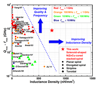 Figure 4 Comparison shows that the vertical magnetic-cored inductor (the star) out-performs the reported state-of-the-art of various magnetic-enhanced inductors.
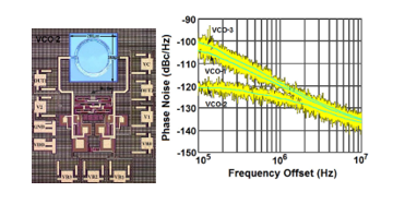 Figure 5 Measurement shows that VCO2 using magnetic-cored inductor has better phase noise performance compared to VCO1/VCO3 using conventional inductors [20].
For complex ICs at advanced nodes, noise coupling mainly occurs in the BEOL stacks through the extremely complex and conductive metal interconnects mesh. This new type of in-BEOL noise coupling is defined as “flying noise”, which is global in nature across the whole chip, and unfortunately, cannot be suppressed by any conventional in-Si noise-isolation techniques. To address this emerging global flying noise challenge, we proposed a novel through-BEOL metal wall flying noise isolation structure as illustrated in Figure 6 [22, 23]. In principle, it is a (near) closed-loop metal wall structure that blocks transmission of electromagnetic waves, hence, noise-isolates circuit blocks residing inside the through-BEOL metal cages. From EM theory, the through-BEOL meta walls can be optimized in terms of metal materials and wall physical designs to block the noise propagation, therefore, eliminating the global flying crosstalk in the BEOL stacks. This flying noise isolation concept was validated experimentally in CMOS. Figure 7 shows the first experiment where a simple amplifier circuit was designed in a foundry 180nm SOI CMOS. A post-CMOS process module was developed to etch a deep trench into the CMOS BEOL stack, which was filled with silver powder to form the in-BEOL metal wall structure. In measurement, it was observed that the troublesome third-order intermodulation interferers were suppressed by about 9dB (Figure 7) [22].
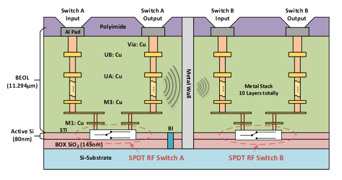 Figure 6 A conceptual X-section view of the new through-BEOL metal wall flying crosstalk isolation structure in SOI CMOS.
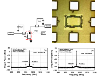 Figure 7 An amplifier circuit with the new in-BEOL metal wall can reduce the IM3 interferers by 9dB in measurement [22].
Figure 8 presents a second prototype design, which are SPDT RF switch circuits fabricated in a foundry 45nm SOI CMOS [23]. The design splits include SPDT switches with and without in-BEOL metal walls that were made of silver nano powders.
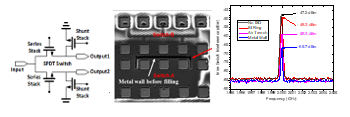 Figure 8 SPDT RF switches fabricated in a 45nm SOI CMOS utilizes the new through-BEOL metal wall to successfully block the global flying crosstalk by 98% in linear scale [23].
Measurement shows that the in-BEOL metal wall structure reduces the inter-switch flying crosstalk by 18.5dB, almost entirely blocked the global flying crosstalk (~98.6% in linear scale). The experiments confirmed that our new through-BEOL metal wall flying noise isolation technique is efficient in blocking the above-Si global flying crosstalk.
4. Above-IC Nano-Crossbar ESD Protection
Electrostatic discharge (ESD) failure is the most devastating reliability problem to ICs. On-chip ESD protection is required for all ICs and electronic systems [24]. As IC process technologies continue scaling and chip complexity rapidly increases, on-chip ESD protection design emerges as a major IC reliability design challenge. Since the initial ESD awareness in late 1960s, ESD protection has been relied on in-Si PN-junction-based active devices to form low-impedance conduction channels to discharge fast ESD transients, hence, provide ESD protection for ICs. Unfortunately, the conventional ESD protection structures inevitably introduce parasitic effects inherent to the PN junctions, such as ESD-induced parasitic capacitance, noises and leakage current, which seriously affect IC performance, particularly for high-frequency broad band RF ICs and high-speed ICs. On the other hand, on-chip ESD protection structures consume large Si die area in order to handle the significant ESD-related energy, and the typically irregular ESD device shapes makes IC physical layout design truly challenging. These ESD protection design problems are becoming unbearable to advanced ICs at sub-28nm nodes. It is hence imperative to develop disruptive ESD protection solutions for future chips that are not tied to in-Si PN junctions [25]. To address such emerging ESD protection design challenges, we devised two revolutionary above-IC non-PN type ESD protection concepts and device structures. Figure 9 depicts the first concept of an above-IC nano-crossbar array ESD protection structure [26-28]. In principle, this new device is a two-terminal phase-changing switch structure comprising two electrodes and a phase-changing insulator in between. The insulator is made of specially synthesized nano materials that is electrically OFF in normal IC operations. Under ESD stressing, the strong incident electrostatic force causes phase change of the nano insulator, making it conducting, hence turns ON the nano crossbar switch structure to discharge the ESD transients. When an ESD event is over, the switch will return to its OFF state. The nano crossbar array switch
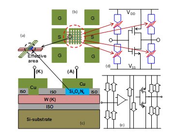 Figure 9 A conceptual illustration for the new above-IC nano crossbar array ESD protection structure in CMOS.
is built in the CMOS BEOL stack above the Si substrate and is not a conventional PN junction device. It is an above-IC ESD switch structure. While each crossbar node is a nano device, a large nano crossbar array can be designed to handle large ESD energy collectively. This novel nano crossbar array ESD switch structure was experimentally validated using a post-CMOS process module developed. Figure 10 presents the measured transient ESD I-V curve for a single-node crossbar ESD switch by transmission-line pulsing (TLP) ESD testing, showing the desired symmetrical two-directional ESD discharging I-V behavior. Figure 11 shows the measured I-C curves for a nano crossbar array ESD switch where multiple ESD triggering effect can be observed. Measurement shows ultrafast ESD response time of ~100pS, negligible leakage current of Ileak~2pA (Figure 12), tunable ESD triggering voltage Vt1 of 1.26~28.3V (Figure 13) and ultrahigh ESD protection capability of ~267V/mm2. Since the new nano crossbar ESD protection structure is above the Si substrate, it does not consume extra Si die area. This novel above-IC nano crossbar array ESD switch structure can potentially resolve all challenging problems associated with the conventional in-Si PN-based ESD protection structures.
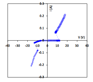 Figure 10 TLP testing shows symmetric ESD discharging I-V curve for a single-node nano crossbar ESD protection structure.
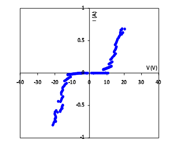 Figure 11 TLP testing shows symmetric ESD discharging I-V curve for a sample nano crossbar array ESD protection structure.
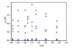 Figure 12 Measurement shows ultralow leakage currents, due to the non-PN ESD structure, for sample nano crossbar ESD protection structures.
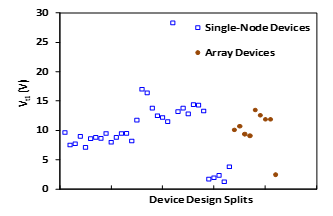 Figure 13 Measurement shows tunable ESD triggering voltage for sample nano crossbar ESD protection structures.
5. Above-IC Graphene NEMS ESD Switch
Figure 14 shows the second novel above-IC ESD protection structure, which is a graphene-based NEMS (gNEMS) switch ESD protection device fabricated in the CMOS BEOL stack [29, 30]. This new graphene gNEMS ESD switch is a two-terminal device, entirely different from conventional in-Si PN-based ESD protection devices. A gNEMS has a graphene membrane over a cavity. The two electrodes are the graphene membrane on top (cathode, or, K) and the bottom of the cavity (anode, or, A). Unlike any PN-based electronic devices, the gNEMS device is a mechanical switch, which remains electrically OFF in normal IC operations. When an ESD transient appears, the electrostatic force pulls the graphene membrane downward to touch the bottom conductor, hence turns on the gNEMS device to discharge the ESD surge. When the ESD transient is over, the graphene film will bounce back and turns the gNEMS OFF again. Since gNEMS is a mechanical switch, ideally, it has no leakage current and almost no parasitic capacitance. Since it is built in the CMOS BEOL stack, above the IC substrate, gNEMS devices will not consume extra Si die area. Therefore, the gNEMS ESD switch is an ideal ESD protection structure. Since graphene film is ultralight and has very large Young’s module, the gNEMS switching speed can be extremely fast. Figure 15 presents the measured transient ESD discharging I-V behaviors for a sample gNEMS switch, showing the desired dual-directional and symmetrical I-V characteristic. Measurement also shows negligible leakage current of ~3pA, superfast ESD response time of ~200ps and ultrahigh ESD protection capability of ~1500V/mm2, which is many orders of magnitude higher than a silicon-controlled rectifier (SCR) ESD protection structure that is normally considered the most robust Si ESD protection structure. It is encouraging that the gNEMS ESD switch can be potentially ideal ESD protection solution for future ICs.
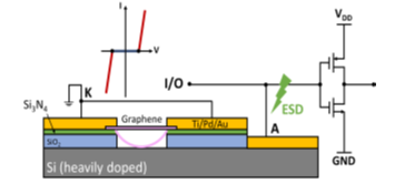 Figure 14 A conceptual illustration for the new above-IC gNEMS ESD switch device in CMOS.
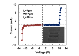 Figure 15 TLP testing shows a dual-directional ESD discharging I-V curve for a sample gNEMS ESD switch, where the inset is a SEM image for gNEMS.
6. Multiple-Gated MOSFETs
Our information and internet era rely on binary data processing, including computing and storage, which was enabled by transistors and CMOS ICs. The base-2 binary numbering system is the foundation for most information processing systems, whose capacity is certainly limited, i.e., 2n (n is bit number in a byte) caps binary the information system capacity. The binary numbering system is natural to CMOS ICs because a MOSFET has two conduction states, OFF (0) and ON (1) corresponding to ID = 0 or not. Imagine a base-M numbering system with M>2, where Mn > 2n results in a much bigger system capacity for a given byte size. Research has been done to explore multiple-state-value devices, mainly pursuing for unique conducting materials to realize many-status logics. As a potential solution, we proposed a novel individually-controlled multiple-gated MOSFET structure. Figure 16 depicts such a device concept where a MOSFET has four individually controlled gates over the same conduction channel. By selectively biasing the four gates, individually or collectively, this MOSFET will deliver multiple conduction states, hence, forms a non-binary Mn numbering system [31, 32]. For different channel conduction states, ID will be different for the MOSFET. By designing the 4-gated MOSFET, 5<M<16 may be obtained. There are several advantages for this base-M information MOSFET structure and numbering system. First, its information system capacity increases significantly from the binary system. Second, by choosing M=10 through device design, a base-10 (i.e., 10n) system may be realized, which not only dramatically increases the system capacity, but also makes computing algorithm and system architecture more natural to human instinct. Third, this 4-gated MOSFET can be fabricated using classic CMOS IC technologies through 3D heterogeneous integration.
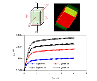 Figure 16 Conceptual illustration for the novel multiple-gated MOSFET.
7. Summary
The past six decades have witnessed the unprecedent advances of the Si-based IC technologies, which has completely changed human life. As we are rapidly moving from the information technology (IT) era to the internet-of-everything (IoET) age, it calls for disruptive IC technologies to facilitate the emerging needs for information sensing, computing, storage and communications, which simply cannot be supported by the hallmark Si planar IC process technologies. To break the deadlock of space, complexity and performance of ICs, one viable answer to the grand technical challenge is to develop smart future chips that can integrate more device functionalities, in a 3D fashion, to improve operating characteristics of IC chips. 3D heterogeneous structures and heterogeneous integration are the potential solutions to continuous advances of Si-based CMOS ICs beyond the Moore’s Law. This paper reviews some novel 3D heterogeneous structures that we developed recently to address the emerging IC design challenges including: compact inductors with vertical magnetic cores, in-BEOL global flying noise isolation structures, on-chip ESD protection and multi-gated transistors for non-binary numbering systems. These new 3D heterogenous structure concepts, while being exemplar, are truly disruptive and potentially enablers for future smart chips.
Conflict of Interest
The authors declare no conflict of interest.
Acknowledgment
The authors acknowledge National Science Foundation for partial supports of the related research.
- G. E. Moore, “Cramming more components onto integrated circuits”, Electronics, pp. 114-117, April 19, 1965. DOI: 10.1109/N-SSC.2006.4785860
- SIA National Technology Roadmap for Semiconductor (NTRS)
- SIA International Technology Roadmap for Semiconductor (ITRS)
- SIA International Technology Roadmap for Semiconductor 2.0 (ITRS 2.0), 2015 Edition.
- ITRS wensite, http://www.itrs2.net/
- Heterogeneous Integration Roadmap (HIR), 2019 Edition.
- Heterogeneous Integration Roadmap (HIR) website, https://eps.ieee.org/technology/heterogeneous-integration-roadmap/2019-edition.html
- Z. A. Ye, S. Almeida, M. Rusch, A. Perlas, W. Zhang, U. Sikder, J. Jeon, V. Stojanović, and T.-J. K. Liu, “Demonstration of 50-mV Digital Integrated Circuits with Microelectromechanical Relays”, in IEEE IEDM Tech Digest, 2018. DOI: 10.1109/IEDM.2018.8614663
- C. Li, F. Zhang, M. Di, Z. Pan and A. Wang, “Developing 3D Heterogeneous Structures for Future Chips”, in Proc. IEEE International Conference on IC Design and Technology (ICICDT), pp.48-51, 2019. DOI: 10.1109/ICICDT.2019.8790942
- C. Yang, F. Liu, T. Ren, L. Liu and A. Wang, “On-Chip Integrated Inductors with Ferrite Thin-films for RF IC”, in IEEE IEDM Digest, pp.225-228, 2006. DOI: 10.1109/IEDM.2006.347003
- J. Zhan, C. Yang, X. Wang, Q. Fang, Z.T. Shi, Y. Yang, T.-L. Ren, A. Wang, Y.H. Cheng, L.-T. Liu, “Stacked-spiral RF inductors with vertical nanoparticle magnetic core for radio-frequency integrated circuits in CMOS”, Sensors & Actuators: A. Physical, V195, pp. 231-238, June 2013. http://dx.doi.org/10.1016/j.sna.2013.02.030
- Z. Ni, J. Zhan, Q. Fang, X. Wang, Z. Shi, Y. Yang, T.-L. Ren, A. Wang, Y. Cheng, J. Gao, X. Li, and C. Yang, “Design and Analysis of Vertical Nanoparticles- Magnetic-Cored Inductors for RF ICs”, IEEE Trans. Electron Devices, 60(4), pp. 1427-1435, April 2013. DOI: 10.1109/TED.2013.2245418
- J. Zhan, C. Yang, X. Wang, F. Zhang, T.L. Ren, A. Wang, Y. Yang, L. T. Liu, L. W. Yang and Z. X. Yue, “Stacked-Spiral RF Inductor with Vertical Nano-Powder-Magnetic-Core in CMOS”, IEEE Microwave and Wireless Components Letters, 22(1), pp.29-31, January 2012. DOI: 10.1109/LMWC.2011.2176474
- C. Yang, F. Liu, X. Wang, J. Zhan, A. Wang, T-L. Ren, L-T. Liu, H. Long, Z. Wu, X. Li, “Investigation of on-Chip Soft-Ferrite-Integrated Inductors for RF ICs — Part I: Design and Simulation”, IEEE Trans. Electron Devices, 56(12), pp.3133-3140, December 2009. DOI: 10.1109/TED.2009.2033328
- C. Yang, F. Liu, X. Wang, J. Zhan, A. Wang, T-L. Ren, L-T. Liu, H. Long, Z. Wu, X. Li,, “Investigation of on-Chip Soft-Ferrite-Integrated Inductors for RF ICs — Part II: Experiments”, IEEE Trans. Electron Devices, 56(12), pp. 3141-3148, December 2009. DOI: 10.1109/TED.2009.2033413
- C. Yang, F. Liu, T. Ren, L. Liu, G. Chen, X. Guan, A. Wang and H. Feng, “Ferrite-Integrated on-Chip Inductors for RF ICs “, IEEE Electron Device Letters, 28(7), pp.652-655, July 2007. DOI: 10.1109/LED.2007.900299
- C. Yang, F. Liu, T-L. Ren, L-T. Liu, G. Chen, X-K. Guan, A. Wang and Z-X. Yue, “Ferrite-Partially-Filled on-Chip RF Inductor Fabricated Using Low-Temperature Nano-Powder-Mixed-Photoresist Filling Technique for Standard CMOS”, in IEEE IEDM Tech. Digest, pp1038-1040, 2007. DOI: 10.1109/IEDM.2006.347003
- H. Long, Z. Feng, H. Feng and A. Wang, “A novel accurate PEEC-based 3D modeling technique for RF devices of arbitrary conductor-magnet structure”, Microwave and Optical Technology Letters, 38(3), Wiley & Sons, pp237-240, August 2003.
- H. Long, Z. Feng, H. Feng, A. Wang, T. Ren, J. Bao, F. Liu, C. Yang, X. Zhang, “A New Modeling Technique for Simulating 3D Arbitrary Conductor-Magnet Structures for RFIC Applications”, IEEE Tans. Electron Devices, 52(7), pp. 1354-1363, July 2005. DOI: 10.1109/TED.2005.850662
- H. Cai, Y. Yang, N. Qi, X. Chen, H. Tian, Z. Song, Y. Xu, C-J. Zhou, J. Zhan, A. Wang, B. Chi and T-L. Ren, “A 2.7-mW 1.36–1.86-GHz LC-VCO With a FOM of 202 dBc/Hz Enabled by a 26%-Size-Reduced Nano-Particle-Magnetic-Enhanced Inductor”, IEEE Trans. Microwave Theory and Techniques, 62(5), pp. 1221-1228, May 2014. DOI: 10.1109/TMTT.2014.2312886
- R. Ma, F. Lu, Q. Chen, C. Wang, F. Liu , W. Zou and A. Wang, “A 2.22–2.92GHz LC-VCO Demonstrated with An Integrated Magnetic-Enhanced Inductor in 180nm SOI CMOS”, in Proc. IEEE RFIC Symp., pp.110-113, 2016. DOI: 10.1109/RFIC.2016.7508263
- C. Wang, Q. Chen, F. Lu, C. Li, F. Zhang and A. Wang, “Blocking Flying Crosstalk in BEOL Validated in Antenna Switches in 45nm SOI CMOS”, IEEE Microwave and Wireless Components Letters, 28(11), pp.1005-1007, November 2018. DOI: 10.1109/LMWC.2018.2873197
- F. Lu, Q. Chen, C. Wang, F. Zhang, C. Li, R. Ma, X. S. Wang and A. Wang, “In-Die Through-BEOL Metal Wall for Noise Isolation in 180nm FD-SOI CMOS”, IEEE Electron Device Letters, 38(5), pp.630-632, May 2017. DOI: 10.1109/LED.2017.2682819
- A. Wang, On-Chip ESD Protection for Integrated Circuits, Kluwer, Boston, 2002.
- A. Wang, H. Feng, R. Zhan, H. Xie, G. Chen, Q. Wu, X. Guan, Z. Wang and C. Zhang, “A review on RF ESD protection design”, IEEE Trans. Electron Devices, 52(7), pp.1304-1311, July 2005. DOI: 10.1109/TED.2005.850652
- L. Wang, X. Wang, Z. Shi, R. Ma, J. Liu, Z. Dong, C. Zhang, L. Lin, H. Zhao, L. Zhang, Y. Cheng, R. Huang and A. Wang, “Dual-Directional Nano Crossbar Array ESD Protection Structures”, IEEE Electron Device Letters, 34(1), pp.111-113, January 2013. DOI: 10.1109/LED.2012.2222337
- L. Lin, L. Zhang, X. Wang, J. Liu, H. Zhao, H. Tang, Q. Fang, Z. Shi, R. Huang, Y. Cheng and A. Wang,, “Novel Nanophase-Switching ESD Protection”, IEEE Electron Device Letters, 32(3), pp.378-380, March 2011. DOI: 10.1109/LED.2010.2099100
- L. Zhang, R. Huang, D. Gao, D. Wu, Y. Kuang, P. Tang, W. Ding, Y. Wang and A. Wang, “Unipolar Resistive Switch Based on Silicon Monoxide Realized by CMOS Technology”, IEEE Electron Device Letters, 30(8), pp.870-872 ,August 2009. DOI: 10.1109/LED.2009.2024650
- R. Ma, Q. Chen, W. Zhang, F. Lu, C. Wang, A. Wang, Y. H. Xie and H. Tang, “A Dual-Polarity Graphene NEMS Switch ESD Protection Structure”, IEEE Electron Device Letters, 37(5), pp. 674-676, May 2016. DOI: 10.1109/LED.2016.2544343
- W. Zhang, R. Ma, Q. Chen, M. Xia, J. Ng, A. Wang and Y-H. Xie, “The electro-mechanical responses of suspended graphene ribbons for electrostatic discharge applications”, Applied Physics Letter, 108, 153103 (2016). http://dx.doi.org/10.1063/1.4946007
- A. Wang, “Novel 3D 4-Gate MOSFET and 5-ary Logic for Hi-density Hi-speed Memory”, a proposal to SRC, Sept. 2003.
- C. Li, F. Zhang, M. Di, Z. Pan and A. Wang, “Advances in 3D Heterogeneous Structures and Integration for Future ICs”, in Proc. IEEE SOI-3D-Subthreshold Microelectronics Technology Unified Conference (S3S), 2019.