Linear Logic Synthesis of Multi-Valued Sequential Circuits
Volume 4, Issue 6, Page No 430-442, 2019
Author’s Name: Nikolay Butyrlagin1,a), Nikolay Chernov1, Nikolay Prokopenko1,2, Vladislav Yugai1
View Affiliations
1Information System and Radio Engineering Department, Don State Technical University, Gagarin Sq. 1, Rostov-on-Don, 344000, Russia
2Institute for Design Problems in Microelectronics of Russian Academy of Sciences, IPPM RAS, Zelenograd, 124681, Russia
a)Author to whom correspondence should be addressed. E-mail: butyrlagin@gmail.com
Adv. Sci. Technol. Eng. Syst. J. 4(6), 430-442 (2019); ![]() DOI: 10.25046/aj040654
DOI: 10.25046/aj040654
Keywords: Memory element, Logic operation, Linear representation, Truncated difference operation, Comparison operation, Circuitry implementation

Export Citations
The basics of unconventional design of current circuits of two-valued and multi-valued memory elements (ME) for storing current digital signals and flip-flops of the main types on their basis are considered. A nontraditional method of ME synthesis is proposed, which is based on the mathematical tool of linear algebra. Linear equations, structural and functional schemes of the main types of logic elements for the construction of ME are given. CMOS-circuitry of various versions of realization of linear logic elements of multi-valued MEs is considered. The comparative analysis is carried out and advantages and disadvantages of linear realization of current two-valued memory elements and flip-flops on their basis in comparison with potential (Boolean) realization are defined. The forecast of merits and demerits of linear implementation of multi-valued memory elements is given
Received: 02 October 2019, Accepted: 10 December 2019, Published Online: 25 December 2019
1. Introduction
Nowadays a potential logic and its mathematical tool, that is Boolean algebra, dominate in the world of logic synthesis of products of microelectronics. We sweepingly accept this fact and appreciate its contribution to digital electronics development.
However, as long as Boolean algebra exists, there have been attempts to replace it by another mathematical tool. It results in efforts to apply spectral transformations of Krestenson, Walsh, Haar [1-5], polynomial representations [6-9] for logic synthesis.
The authors of this article suggest applying mathematical tool of linear algebra for the aims of logic synthesis [10]. As a result of investigations, we have defined primary application domain of this tool that is current circuits of random valuedness. The Boolean algebra is not convenient to synthesize multi-valued digital circuits, so linear algebra is not an opponent to the Boolean algebra despite the specific nature of the logic synthesis process and multi-valued digital circuits circuitry [11-19]; it is rather an addition to Boolean algebra .
The authors have developed:
Mathematical tool and methods of linear logical synthesis of two-valued and multi-valued digital structures;
circuit solutions of the basic logic elements for constructing digital structures;
circuitry solutions of some digital combinational two-valued and multi-valued structures (adders, decoders, multiplexers, digital components of the ADC, etc.);
In the process of research, the computer simulation of two-valued and multi-valued logical elements proved their operational integrity [20 – 27]. The effectiveness of linear algebra as a mathematical tool of logical synthesis is confirmed by patents RU2506695, RU2509412, RU2514789, RU2547225, RU2553070, RU2549144 and publications [20 – 27].
The results of research show the advantages of the proposed design methodology over the Boolean: it enables to suggest logic elements with improved characteristics compared to Boolean elements, as well as workable multi-valued elements. The purpose of this article is to demonstrate the possibilities of using current logic (linear algebra) as a mathematical tool for logical synthesis and circuit design of sequential two-valued and multi-valued digital structures using current flip-flops as an example.
Methodology
At the beginning, the well-known structural schemes of potential flip-flops of the main, widely used types are given. Then, structural schemes of their two-valued current analogues are synthesized. Further, the features of the structural completeness of multi-valued flip-flops and their circuitry implementation are considered.
Two-valued potential flip-flops. Two-valued flip-flops have a quit wide classification [11, 12]. RS-, D-, T- and JK-flip-flops are the most commonly used two-valued flip-flops. A brief description of the structural implementation of these flip-flops is given below.
Asynchronous RS-flip-flop is a tandem amplifier with positive feedback. Its structural circuit, implemented on AND-NOT (OR-NOT) elements is in Fig. 1 а, and its logic symbol is in Fig. 1 b.
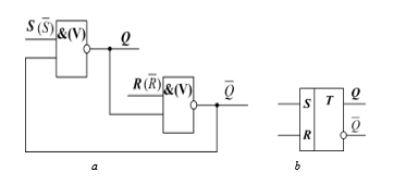 Figure 1: Structural circuit (а) and logic symbol (b) of RS-flip-flop on OR-NOT (AND-NOT) elements.
Its structural circuit, implemented on inhibit circuit (“implication gate”) is shown in Fig. 2 а, its logic symbol is shown in Fig. 2 b.
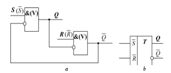 Figure 2: Structural circuit (а) and logic symbol (b) of RS-flip-flop on implication gates (inhibit circuits).
Single-ended synchronous RS-flip-flop is characterized by additional synchronization input. The flip-flop is switched to opposite state, if there is enabling level of signal at synchronization input. Its logic symbol is shown in Fig. 3.
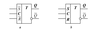 Figure 3: Logic symbol of single-ended synchronous RS-flip-flops: a – on OR elements, b – on AND elements
To eliminate disadvantages of single-ended RS-flip-flop’s switch [12] the push-pull circuits are used. Their structures, implemented on AND-NOT (OR-NOT) elements are in Fig. 4 а, b.
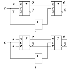 Figure 4: Structural circuits of push-pull RS-flip-flops.
The logic symbol of push-pull RS-flip-flops is in Fig. 5.
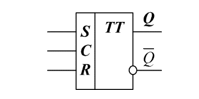 Figure 5: Logic symbol of push-pull RS-flip-flop.
Now let us show the structures of flip-flops of other popular types. The D-flip-flop structural circuit is shown in Fig. 6 а, its logic symbol is shown in Fig. 6 b.
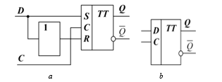 Figure 6: D-flip-flop: а – structural circuit, b – logic symbol.
The structural circuit of Т-flip-flop is shown in Fig. 7 а and its logic symbol is shown in Fig. 7 b.
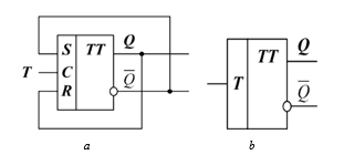 Figure 7: Т-flip-flop: а – structural circuit, b – logic symbol.
And finally, the structural circuit of JK-flip-flop is in Fig. 8.
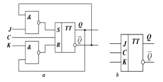 Figure 8: JK-flip-flop: а – structural circuit, b – logic symbol.
Two-valued current flip-flops. The potential flip-flops are similar to current flip-flops at system technology level, so it is possible to show the current asynchronous structural circuit of RS-flip-flop in the form, shown in Fig. 9, and its logic symbol – in the form, specified in Fig. 10 [21].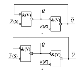 Figure 9: Structural circuit of two-valued asynchronous RS-flip-flop on AND-NOT (OR-NOT) current elements: а – output implementation, b – input implementation.
In the structural and functional diagrams given hereinafter, arrows indicate the directions of the current input and output signals: incoming arrows indicate input currents, outcoming arrows indicate output currents. The type of implementation of the element (incoming or outcoming) is determined by the direction of the output signal of the element.
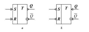 Figure 10: Logic symbol of two-valued asynchronous RS-flip-flop on AND-NOT (OR-NOT) current elements: а –output implementation, b – input implementation.
Possible differences in the options for implementing flip-flop circuits appear at the levels of functional and circuit design.
The structural circuit of synchronous RS-flip-flop is in Fig. 11 and its logic symbol is in Fig. 12.
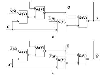 Figure 11: Structural circuit of two-valued synchronous RS-flip-flop on AND-NOT (OR-NOT) current elements: а –output implementation, b – input implementation.
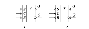 Figure 12: Logic symbol of two-valued asynchronous RS-flip-flop on AND-NOT (OR-NOT) current elements: а – output implementation, b – input implementation.
Similarly, structural implementation of push-pull current synchronous RS-flip-flop is similar to corresponding potential circuit. The structures of synchronous push-pull RS-flip-flops are in Fig. 13 and their logic symbols – in Fig. 14. The “+” element performs the function of an inverter.
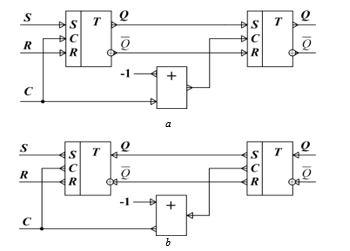 Figure 13: Structural circuits of push-pull synchronous current RS-flip-flops: а – output implementation, b – input implementation.
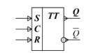 Figure 14: Logic symbol of push-pull synchronous current RS-flip-flops
The structural implementations for flip-flops of other types are also similar to implementations of corresponding potential circuits.
Three-valued flip-flops
Multi-valued flop-flops. Usually the multi-valued digital circuits are considered as generalization of corresponding two-valued circuits [1]. But bivalent logic degeneracy causes problems for such generalization. The primary difficulties of multi-valued flip-flop synthesis are the following:
– selection of logic valuedness, which is suitable to construct multi-valued memory elements;
– selection of multi-valued equivalents of logic operations, applied for logic synthesis of memory elements in two-valued logic;
multi-valued interpretation of inversion.
Let us consider the above problems in details.
As to select logic valuedness to construct multi-valued flip-flops we should note the following. One uses concept of structural completeness (transition and outputs system completeness) for flip-flops, applied as automata memory elements for functional completeness of logic functions (basis) for combinational circuit in automata theory [9]. By default, the flip-flop is characterized by transition and output system completeness, if it is possible to assign some set of control signals to each output state, the said signals transit it from any previous state to the said state within finite number of steps. In two-valued case any known memory elements has this property.
The transition graph of two-valued flop-flop can be represented in the form shown in Fig. 15.
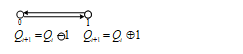 Figure 15: Transition graph of two-valued flop-flop.
In the multi-valued case, the situation is somewhat more complicated.
When k = 3 (Fig. 16), the multi-valued flip-flop can have transition graphs of direct (per neighboring vertex: 0→1→2→0 and through vertex: 0→2→1→0) and reverse (per neighboring vertex: 0→2→1→0 and through vertex: 0→1→2→0) type, which are opposite to each other. They are also complete graphs, covering all vertices, i.e. three-valued flip-flop has transition and output system completeness.
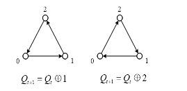 Figure 16: Direct and reverse transition graph for three-valued flip-flop.
When k = 4 (Figure 17), the multi-valued flip-flop can also have direct and reserve graphs.
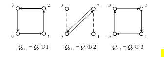 Figure 17: Four-valued memory element transition graphs.
However, from Fig. 17 it follows that the four-valued flip-flop does not have the completeness of the system of transitions and outputs: when passing through two vertices, the transition graph is looped. The transition graphs for k = 5 and k = 7 are in Fig. 18 and Fig. 19.
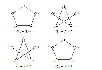 Figure 18: Transition graph of five-valued flip-flop.
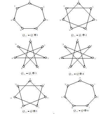 Figure 19: Seven-valued flip-flop transit graph.
The Fig. 15 – 19 show a confirmation of the known fact [9], that the transition and output system completeness of the flip-flop of random valuedness is provided, only when logic valuedness magnitude is a prime number.
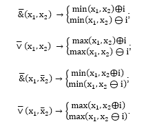
Let us note the following, concerning selection of multi-valued equivalents of two-valued operations, used for memory elements synthesis. The most popular flip-flops for two-valued version are flip-flops, implemented on the elements realizing operations & ̅(x_1,x_2 ) (AND-NOT) and ∨ ̅(x_1,x_2 ) (OR-NOT).
The following operations are functionally close to these operations: & ̅(x_1,x ̅_2 ) (“Inhibit per x_2“) and ∨ ̅(x_1,x ̅_2 ) (“Implication from x_1 to x_2”). Generalization of these operations for multi-valued version results in the following representations:
In current circuits the authors use elements, implementing comparison operations >(x_1,x_2 )), sum module ⨁(x_1,x_2 ) and difference ⊖x_1 x_2 and truncated difference operations.
x_1∸x_2={█(x_1-x_2 when x_1≥x_2@0 when x_1<x_2 )┤.
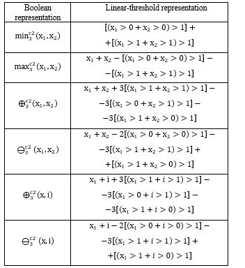
If to combine it with linear space operation, it is possible to have a variety of different presentations for multi-valued equivalents for main two-valued functionally complete system AND, OR, NOT. There are some possible versions of these operations in Tables 1-4.
Table 1: Primary operations, presented through truncated difference
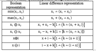
It is possible to synthesize more than 80 different flip-flops, using only set of operations, specified in the above tables, which are required to form logic elements, from which flip-flop memory elements are constructed.
It is necessary to note, that being fully equivalent to AND, OR, NOT operations in two-valued version, in multi-valued case some of these expressions results in functions, different from multi-valued equivalents of AND, OR, NOT operations. This confirms the two-valued logic degeneracy, because multi-valued functional systems, different from traditional nature, are converged to it.
Table 2: Primary operations, presented through sum and difference module
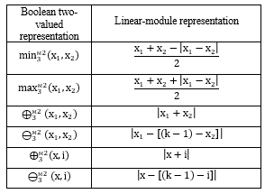
Table 3: Primary operations, presented through comparison operation
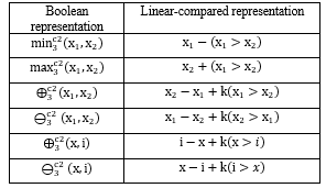
Table 4: Primary operations, presented by threshold form
Finally, on the multi-valued interpretation of inversion. In the two-valued case, the flip-flop consists of two identical logic elements, therefore, you can submit information to the input and “remove” it from the flip-flop output in a direct or inverse code. By controlling the process of recording information in a flip-flop, it is possible to process information by setting a direct or inverse value at the desired output.
A multi-valued flip-flop has k inputs and the same number of outputs. Here, the information processing function is much “richer” than in the two-digit case: controlling the process of recording information in such a flip-flop, it can be cyclically shifted left or right (“rotate”). In the process of information rotating, you must remember that
x⨁i=x⊖(k-i).
This ratio enables, if necessary, to replace one of the operations of the recorded ratio with another.
The synthesis of multivalued flip-flops should also be preceded by an agreement on the principles of generalizing two-valued flip-flops to a multivalued case. The agreement proposed by the authors of this article consists of the following main provisions:
– the number of flip-flop information inputs must be equal to the logic valuedness;
– at the outputs of the flip-flops there must be a full set of logic values (the number of outputs of the flip-flop must be equal to the valuedness of the logic);
– the valuedness of the output signals of the functional elements of the flip-flop should not exceed the valuedness of the logic used.
The listed provisions, as is easy to see, in the two-valued case are fully implemented.
RS flip-flop. A verbal description of the functioning algorithm of a multi-valued RS-flip-flop corresponding to the agreement on the principles of generalizing two-valued flip-flops to a multi-valued case is given below:
– the storage mode corresponds to the values of the input signals S = SR = R = k – 1 (or S = SR = R = 0);
– the signal S increases the flip-flop state index relative to the current state towards the state k-1, the SR signal decreases or increases the current one depending on the ratio of the current state index and the signal value at this input, and the signal R decreases towards the state 0; change of state in a cycle is impossible (let’s leave it for universal flip-flops!);
– the magnitude of the change in the state index is equivalent to the value of the input signal: a signal equivalent to 1 can increase (or decrease) the index of the current state by 1, a signal equivalent to 2 by 2, etc .;
– to change the flip-flop state index relative to the current state i, signal S can take values from 1 to k-1-i (larger values will be equivalent to k-1-i in action), similarly, signal R can take values from 1 to i- 1 (larger values will be equivalent to i -1);
– Allowed combinations of input signal values are all combinations in which one of the input signals is k – 1 (0) and the others take any of the possible values.
The meaning of the last paragraph of the algorithm is that to change the state of the flip-flop, the two inputs must have signals 0 or k-1, which passes the setting signal of any of the allowed values, and the third – the signal that sets the state.
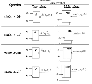
Table 5: Logic symbols for “traditional” multi-valued equivalents of two-valued operations
Results and Discussion
Structural design. The above research results allow us to move to the structural design of current two-valued and multi-valued flip-flops.
In the following exposition, we will mainly confine ourselves to the synthesis of flip-flops with the valuedness k = 2, 3, since reasoning about flip-flops of greater valuedness practically repeats similar arguments about ternary flip-flops. In necessary cases, the features of flip-flops of greater valuedness will be specially discussed.
To construct the structural, functional and basic circuit diagrams of current flip-flops, the above current operations and their combinations, as well as linear space operations, will be used. Moreover, we restrict ourselves to the “traditional” approach, i.e. using operations generalized to the multi-valued case in the “conventional” way.
The logic symbols for “traditional” multi-valued equivalents of above operations are in Table 5.
A base of current operations is the following [min(max)](x_1,x_2 ) and [⊕(⊝)](x,i)operations with different representations, using various current operations. The most important representations (see Tables 1-4) are specified below:
– operation min(x_1,x_2 ):
min(x_1,x_2 )⇒{■(x_1∸(x_1∸x_2 )@(x_1+x_2-|(x_1∸x_2)|)/2@[(x_1+x_2 )>3]+[(2x_1+x_2 )>2] )┤;
– operation max(x_1,x_2 ):
max(x_1,x_2 )⇒
{■(x_1+(x_2∸x_2 )@(x_1+x_2+|x_1∸x_2 |)/2@x_1+x_2-[(x_1+x_2 )>3]-[(x_1+2x_2 )>2] )┤;
– operation ⊕(x,i):
⊕(x,i)⇒{■(i-x+3(x>i)@x+i-k[1∸(k∸(x+i))]@|x+i| )┤;
– operation ⊝(x,i):
⊖(x,i)⇒{■(|x-[(k-1)-i]|@x-i+3(i>x)@|x-i| )┤.
The logic elements, from which the analogues of conventional flip-flops are constructed, are consecutive connection of elements implementing [min(max)](x1,x2) and [⊕(⊝)](x,i) operations.
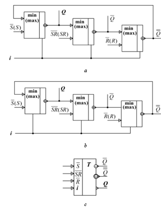 Figure 20: Structural circuit of three-valued RS-flip-flops: а – on [min(max)]⊕i, b – on [min(max)]⊖i , c – logic symbol (output implementation).
 Figure 21: Structural circuits of three-valued asynchronous RS-flip-flops: а – on [min(max)][x_1,⨁(x_2,i)], b – on [min(max)][x_1,⊖(x_2,i)], c – logic symbol (input implementation).
The structural circuit and logic symbol of three-valued asynchonous RS-flip-flop on equivalent elements AND-NOT (OR-NOT) are in Fig. 20-21.
Let us consider functioning of three-valued RS-flip-flop, which structural circuit is shown in Fig. 20 а. It is seen that state storage phase is provided by signals of level 2 (min – realization) or 0 (max – realization) at inputs S, SR, and R.
Let in min implementations of the RS-flip-flop (Fig. 20), at the beginning, the setup signal i is 0, which corresponds to a direct (i.e., without rotation) recording of the value of the input information. When the input signal is set S = 0 – 2 and SR = R = 2, the signal Q ̅=S⨁1is formed at the output of the logic element D2, at the next (D3) – signal Q ̿=Q ̅⨁1, at the last (D1) – signal Q=Q ̿⨁1. For example, at S = 0, the signals Q ̅=1, Q ̿=2, Q=0 (state “0”) are generated at the outputs.
If the setting signal i is 1, which corresponds to the right cyclic shift of the signal by one in each logic element, then the signal S⨁2 is generated at the output of the first logic element D2, − Q ̿=Q ̅⨁2 at the output of the second element (D3), the output of the third (D1) is the signal Q=Q ̿⨁2. For example, with S = 0 and SR = R = 2, the signals Q ̅=2, Q ̿=1, Q=0 (state “0”) are formed at the outputs.
If the setting signal i is 2, which corresponds to the left cyclic shift of the signal by two (to the left cyclic shift by one) in each logic element, then the signal S⨁▒3=S is generated at the output of the first logic element (D2), − Q ̿=Q ̅⨁▒3=Q ̿ at the output of the second element (D3), the signal Q=Q ̿⨁▒3=Q at the output of the third (D1). For example, with S = 0 and SR = R = 2, the signals Q ̅=0, Q ̿=1, Q=2 (state “2”) are formed at the outputs.
Let the flip-flop be in state “1”. In this case, the input signal SR can transit it into any of the remaining states, since this signal determines the value of the output signal of the element D3 and propagates with a shift along the remaining elements of the flip-flop, the input state of the flip-flop cannot be changed, since the second input of the element D3 is 0, and the signal S can transit the flip-flop only in the state “0”.
The graph of changes of the state, when i = 1 is in Fig. 22 а and the process of signal values change on the outputs of logic elements is in Fig. 22 b.
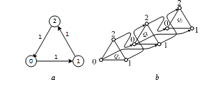 Figure 22: Three-valued RS-flip-flop graph, when i = 1: а – state change, b – output signal value change.
When i = 2, a switch process will go reverse. The graphs of three-valued RS-flip-flop for such case are in Fig. 23.
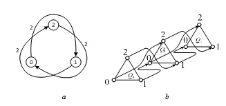 Figure 23: Three-valued RS-flip-flop graphs, when i = 2: а – state change, b – output signal value change.
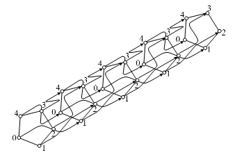 Figure 24: Graph of the value changes of the output signals of five-valued RS-flip-flop i = 1.
Similarly, it is possible to construct graphs for state change and values of flip-flop output signals of higher valuedness. The structure of the graph will change greatly at other values of k. The graph of value changes of the output signals of five-valued flip-plop at i=1 is in Fig. 24 as an example.
Here visualization is lower than the one for three-valued case.
As in two-valued case synchronous single-ended RS-flip flops are characterized by wider functional possibilities. Their main difference from asynchronous flip-flops is an availability of additional synchronization input С, a signal on which defines a flip-flop state change moment, if there is a signal, which is able to result in such change, at informational input (inputs). An input signal is able to be from 0 to k-1 at any input, so signal С should take on value 0 (“lock” input of flip-flop, its state is not changed at any input signal change) or k-1 (any value signal comes to flip-flop input and it goes to the state, corresponding to the said value). It is in good agreement with two-valued flip-flops, if we understand synchronous signal inversion as 1-С, that is (k-1)-C.
It is possible to describe k-valued single-ended synchronous RS-flip-flop as RS-flip-flop, where S-, RS- and R-inputs are connected to S-, RS- and R-inputs of memory element through min or max, where the synchronous signal С is supplied to second inputs.
The RSC-flip-flop structural circuit is in Fig. 25 and its logic symbol is in Fig. 26.
Push-pull circuit of three-valued RSC-flip-flop is constructed from two single-ended RSC-flip-flops similar to two-valued case. Its structural circuit and logic symbol are in Fig. 27.
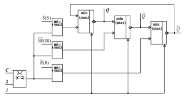 Figure 25: Single-ended RSC-flip-flop structural circuit (AND-NOT – equivalent).
 Figure 26: Logic symbol of three-valued synchronous RSC-flip-flops: а –output implementation, b – input implementation.
The tree-valued single-ended synchronous D-flip-flop is functionally similar to two-valued D-flip-flop: it is set to state, correspodning to input signal value by synchronous signal. In other words, it is possible to describe three-valued D-flip-flop as RS-flip-flop with input signals:
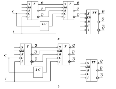 Figure 27: Structural circuit and logic symbol push-pull synchronous RS-flip-flop: а – output implementation, b – input implementation.
S=D;
RS=D⨁i;
R=D⨁i⨁i.
The structural circuit of synchronous single-ended k-valued D-flip-flop (AND-NOT – equivalent) is in Fig. 28.
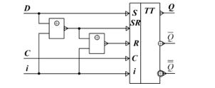 Figure 28: Structural circuit of synchronous single-ended three-valued D-flip-flop.
A structure of OR-NOT – equivalent of three-valued D-flip-flop is of similar form.
The three-valued Т-Flip-Flop is also implemented on two single-ended RS-flip-flop and is counter module 3, an order of counting is defined by value of i. The structural circuit and logic symbol of T-flip-flop are in Fig. 29.
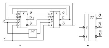 Figure 29: Three-valued push-pull synchronous T-flip-flop: а – structural circuit, b – logic symbol.
The structural circuit of synchronous three-valued push-pull JK-flip-flop is in Fig. 30.
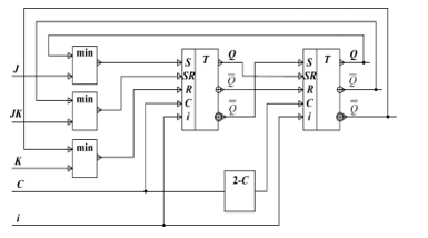 Figure 30: Structural circuit of synchronous three-valued push-pull JK-flip-flop.
We perform circuit design via example of two-valued current flip-flops and their three-valued traditional generalization on the base of conjunctive function representation. Let us consider design of two-valued and three-valued logic elements and the simplest flip-flops. We do not consider circuits of multi-valued flip-flops of higher valuedness because it is quite difficult to show the said circuits within this article.
Two-valued flip-flops. All variants of basic operation representation, specified in Tables 1-4, are suitable for their synthesis.
The following operation is a current equivalent of OR-NOT operation in difference form:
1∸[(x_1+x_2 )∸1].
It is possible to verify its correctness by substitution. The basic diagram of logic element, which implements the said operation, is in Fig. 31.
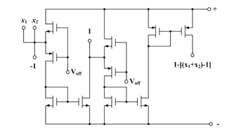 Figure 31: Basic diagram to implement 1∸[(x_1+x_2 )∸1].
Applying module form of current representation results in the following form of OR-NOT operation:
2-x_1-x_2+|x_1-x_2 |.
The basic diagram of OR-NOT operation implementation current variant in module form is in Fig. 32.
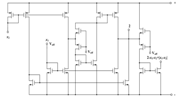 Figure 32: Basic diagram to Implement 2-x_1-x_2+|x_1-x_2 |.
A comparison form of OR-NOT current representation results in the following form:
1-x_2+(x_1>x_2 ).
Its circuit implementation is in Fig. 33.
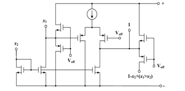 Figure 33: Basic diagram to implement 1-x_2+(x_1>x_2 ).
When combining two elements in amplifier circuit with positive feedback, it results in two-valued RS-flip-flop construction. Its basic diagram is in Fig. 34.
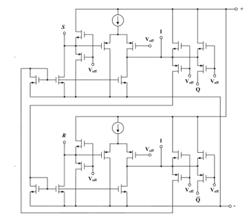 Figure 34: RS-flip-flop basic diagram in comparison representation.
OR-NOT operation threshold current representation results as following:
1-[(x_1+x_2 )>1].
Its circuit implementation is shown in Fig. 35.
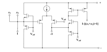 Figure 35: Basic Diagram of OR-NOT operation in threshold representation.
The simple current RS-flip-flop in threshold representation is in Fig. 36.
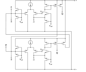 Figure 36: RS-flip-flop basic diagram in threshold representation.
Multi-valued flip-flops are constructed on elements-generalizations of two-valued elements, which implement OR-NOT operation. As we have already said above, the traditional generalizations are consecutive connection of elements [min(max)](x_1,x_2 ) and [⊕(⊝)](x,i), that is min(x_1,x_2 )⊕i, min(x_1,x_2⊕i), and two similar operations, based on ⊝. The operations, specified in Table 3, are not suitable for this purpose, because multiple generalizations are different from traditional ones here. It is better to consider them separately.
Difference representation of min(x_1,x_2 )⊕i is the following:
[x_1∸(x_1∸x_2 )]+i-3〈1∸{3∸[[x_1∸(x_1∸x_2 )]+i]}〉
The implementation circuit for this expression is in Fig. 37.
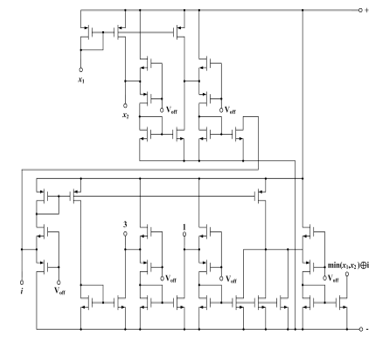 Figure 37: Basic diagram to implement difference representation min(x_1,x_2 )⊕i.
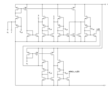 Figure 38: Basic diagram to implement difference representation of min(x_1,x_2⊕i).
A difference representation of min(x_1,x_2⊕i) is the following:
i-[x_1∸(x_1∸x_2 )]+
+3〈1∸{3∸[i∸[x_1∸(x_1∸x_2 )]]}〉
The basic diagram to implement this expression is in Fig. 38.
It is visible that the last circuit is different from the previous one only by order of element sequence of min(x_1,x_2 ) and x⊕i operation implementation.
The circuit implementation of max(x_1,x_2 )⊕i and max(x_1,x_2⊕i) logic elements is in Fig. 39.
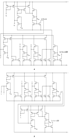 Figure 39: Basic diagram to implement difference representation of operations: а – max(x_1,x_2 )⊕i, b – max(x_1,x_2⊕i).
A module representation of min(x_1,x_2 )⊕i is formed from min(x_1,x_2 ) representation as following:
(x_1+x_2-|x_1-x_2 |)/2
and x⨁i which has the following form:
3-x-i-3|1-i|+3⌈x-|x-i|⌉.
The basic diagram to implement logic element min(x_1,x_2 )⊕i is in Fig. 40.
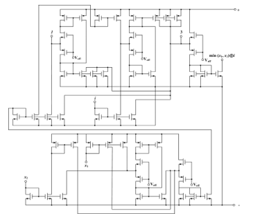 Figure 40: Basic diagram to Implement Difference representation of min(x_1,x_2 )⊕i operation.
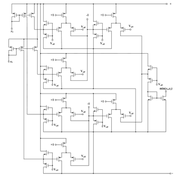 Figure 41. Basic diagram for threshold implementation of min(x_1,x_2 ).
Here the basic diagram to implement min(x_1,x_2⊕i) is an interchange of min(x_1,x_2 ) and x⨁i implementations. Similarly, it is possible to implement max(x_1,x_2 )⊕i and max(x_1,x_2⊕i).
The threshold representation of min(x_1,x_2 ) consists of sum of two threshold functions and can be written as following:
[((x_1>0)+(x_2>0))>1]+[((x_1>1)+(x_2>1))>1],
Its basic diagram is in Fig. 41.
We can describe x⨁i operation as following
x_1+i+3[((x_1>1)+(i>1))>1]-
-3[((x_1>0)+(i>1))>1]-
-3[((x_1>1)+(i>0))>1].
The basic diagram of its implementation is in Fig. 42.
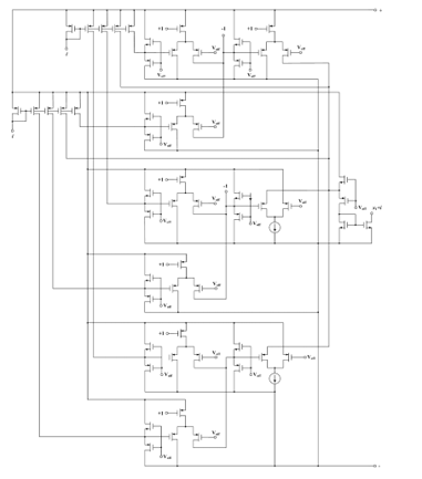 Figure 42: Basic diagram to implement x⨁i .
It is possible to construct logic elements, from which the third-valued flip-flops are constructed, using the above schematic implementations. It is possible to construct flip-flops of different types, following the above structural circuits.
Conclusion
The advantages of using the proposed linear circuitry for the construction of flip-flops can be estimated on the basis that:
– all active circuit elements operate in unsaturated mode, therefore, they have higher performance and other frequency characteristics than potential elements;
– circuits contain only active components (transistors), therefore, they are more technological than potential elements; if, for example, to estimate the technological complexity of the elements of LSI contains one conductor, two transistors, three resistors, the technological complexity of the standard two-input potential inverter (11 links, 5 transistors, 5 resistors) is 36, and the linear threshold analog (6 links, 8 transistors) is 22, that is a third less!
– the basis for the construction of the equations of functioning of logic elements is their difference construction, in which the output signal of the element is the difference of the incoming and outcoming components, therefore, linear logic elements have better performance characteristics;
A possible negative indicator of linear circuits may be their energy characteristics: the condition for the operation of the circuits is a constant flow of current in their circuits. However, at high frequencies, these characteristics are likely to differ little from similar characteristics of potential circuits.
Multivalued current logic elements are a new class of elements, which has no analogue in potential logic and there is simply nothing to compare the characteristics of current elements with. Its advantages and disadvantages are all of the above positive and negative qualities of linear circuits, presumably a linear increase in hardware costs for the implementation of schemes with increasing valuedness, as well as the reality of creating a fully functional multi-valued logic elements and digital structures based on them.
Conflict of Interest
The authors declare that there is no conflict of interests regarding publication of this paper.
Acknowledgments
The reported study was funded by RFBR according to the research project No. 18-37-00061.
- S.V. Yablonsky, “An introduction to mathematical mathematics,” Textbook A manual for universities, 2nd ed, Moscow publ. Nauka, 1986, 384 p. (in Russian).
- M.G. Karpovsky, E.S. Moskalev, “Spectral methods of analysis and synthesis of discrete devices,” Moscow, Energy, 1973 – 144 p. (in Russian).
- V.D. Efremov, A.A. Kuzmin, V.A. Stepanov, “Calculation of logical functions using the Rademacher transforms,” Automation and Telemechanics, 1984, No. 2. (in Russian).
- V.P. Shmerko, “Synthesis of arithmetic forms of Boolean functions by means of the Fourier transform,” Automation and Remote Control. 1989. No. 5. pp. 134-142. (in Russian).
- T.I. Post, “Introduction to a genetal theory of elementary propositions,” Math, 1921, 43, No.3, p.163-185. (in Russian).
- L. A. Zalmanson, “Fourier transform, Walsh, Haar and their application in management, communications and other fields,” Moscow, Nauka, Fizmatlit publ., 1989, 496 p. (in Russian).
- V.L. Artyukhov, V.N. Kondratiev, A.A. Shalyto, “Realization of Boolean functions by arithmetic polynomials,” Automation and Telemechanics. 1988, No. 4, pp. 1-48. (in Russian).
- V.D. Malyugin, G.A. Kukharev, V.P. Shmerko, “Transformation of polynomial forms of Boolean functions,” Moscow, Institute of Management Problems, 1986. (in Russian).
- V. Malyugin, “Implementation of Boolean functions by arithmetic polynomials,” Automation and Telemechanics, 1982, No. 4, pp. 84–93 (in Russian).
- N.N. Prokopenko, N.I. Chernov, V.Ya. Yugai, “Base Concept of Linear Synthesis multi-Valued Digital Structures within Linear Spaces” Proceedings of The IS&IT13 Congress., The Scientific Edition in four volumes, Moscow, PhisMathLit, 2013, vol. 1, pp. 284-289. (in Russian)
- E.P. Ugryumov, “Digital circuitry,” BHV Publ, St. Petersburg, 2000, 528 p. (in Russian).
- I.N. Bukreev et al, “Microelectronic circuits of digital devices,” Moscow, Radio and communications, 1990, 416 p. (in Russian).
- A.F. Gonzalez and P. Mazumder, “Multiple-valued signed digit adder using negative differential resistance devices”, in IEEE Transactions on Computers, vol. 47, no. 9, pp. 947-959, Sept. 1998. DOI: 10.1109/12.713314
- A. Morgul and T. Temel, “Current-mode level restoration: circuit for multi-valued logic”, in Electronics Letters, vol. 41, no. 5, pp. 230-231, 3 March 2005. DOI: 10.1049/el:20056998
- P. Gonga, “Quaternary logic and applications using Multiple Quantum well based SWSEETs”, IEEE VLSICS, vol. 3, no. 5, pp. 27-42, Oct. 2012. DOI : 10.5121/vlsic.2012.3503
- Ch. Babu Dara, T.Haniotakis, S.Tragoudas, “Delay analysis for an N-Input current mode threshold logic gate”, Computer Society Annual Symposium on VLSI 2012 IEEE, DOI: 10.1109/ISVLSI.2012.34
- K. Navi, “A Novel Current Mode Full Adder Based on Majority Function”, World Applied Sciences, Journal 4 (5): 676-680, 2008.
- N.K. Naware, D.S. Khurge and S.U. Bhandari, “Review of Quaternary Algebra & Its Logic Circuits”, 2015 IEEE ICCUBEA, 2015, pp. 969-973. DOI: 10.1109/ICCUBEA.2015.204
- B. Kishor, “Implementation of Ternary / Quaternary Addition using Multivalue Logic Digital Circuit”, International Journal of Computer Application, vol. 118, no. 4, May 2015.
- N.N. Prokopenko, N.V. Butyrlagin, N.I. Chernov, V.Ya. Yugay, “Synthesis of binary flip-flops in the apparatus of linear algebra,” News SFU, Technical science, No. 2. 2015, pp. 115-125. (in Russian).
- N.N. Prokopenko, N.I. Chernov, V.Ya. Yugay, N.V. Butyrlagin, “Linear synthesis of a k-digit digital element base with current logical signals: the principle of generalization,” Problems of developing promising micro- and nanoelectronic systems, 2016 Proceedings under the general. ed. Academician of the RAS A.L. Stempkovsky, Moscow publ, IPPM RAS, 2016, Part I. P. 70-77. (in Russian).
- N.I. Chernov, V.Y. Yugai, N.N. Prokopenko, N.V. Butyrlagin, “Basic concept of linear synthesis of multivalued digital structures in linear spaces,” Proceedings of IEEE East-West Design and Test Symposium, EWDTS 2014, art. no. 7027045. DOI: 10.1109/EWDTS.2014.7027045
- N.N. Prokopenko, N.V. Butyrlagin, N.I. Chernov, V.Ya. Yugai, “The linear concept of logical synthesis of digital IP-modules of control and communication systems,” Proceedings of International Siberian Conference on Control and Communications, SIBCON 2015, art. no. 7147182. DOI: 10.1109/SIBCON.2015.7147182.
- N.N. Prokopenko, N.V. Butyrlagin, N.I. Chernov, V.Ya. Yugai, “Basic linear elements of k-Valued digital structures,” Proceedings of International Conference on Signals and Electronic Systems, ICSES 2016, pp. 7-12. DOI: 10.1109/ICSES.2016.7847763.
- N.N. Prokopenko, N.I. Chernov, V. Yugai, N.V. Butyrlagin, “The element base of the multivalued threshold logic for the automation and control digital devices,” Proceedings of 2017 IEEE International Siberian Conference on Control and Communications, SIBCON 2017, art. no. 7998508. DOI: 10.1109/SIBCON.2017.7998508.
- N.N. Prokopenko, N.I. Chernov, V. Yugai, N.V. Butyrlagin, “The multifunctional current logical element for digital computing devices, operating on the principles of linear (not boolean) algebra,” Proceedings of 2016 IEEE East-West Design and Test Symposium, EWDTS 2016, art. no. 7807723. DOI: 10.1109/EWDTS.2016.7807723.
- N. Chernov, N. Prokopenko, V. Yugai, N. Butyrlagin “Linear algebra as an alternative approach to the synthesis of digital devices of automation and control systems”, Advances in Science, Technology and Engineering Systems Journal, vol. 3, no. 1, pp. 168-190 (2018).
Citations by Dimensions
Citations by PlumX
Google Scholar
Scopus
Crossref Citations
- N. I. Chernov, A. I. Gulin, N. V. Butyrlagin, N. N. Prokopenko, "Features of a Multivalued Generalization of Binary Logic Operations in Linear Algebra for Problems of Digital Processing of Current-Output Sensor Signals." Automation and Remote Control, vol. 82, no. 12, pp. 2213, 2021.
No. of Downloads Per Month
No. of Downloads Per Country