
Design and Analysis of Frequency Reconfigurable Antenna Embedding Varactor Diodes
Volume 4, Issue 6, Page No 371-376, 2019
Author’s Name: El Mustapha Iftissane1, Moulay Driss Belrhiti², Seddik Bri2,a), Jaouad Foshi1, Nawfal Jebbor1
View Affiliations
1Electronics, Instrumentation and Measurement Physics Team, Faculty of Sciences and Technics, Moulay Ismail University of Meknes,Errachidia, Morocco
2Material and Instrumentations Team,Electrical Engineering Department, ESTM, Moulay Ismail University of Meknes, Meknes, 50000, Morocco
a)Author to whom correspondence should be addressed. E-mail: briseddik@gmail.com
Adv. Sci. Technol. Eng. Syst. J. 4(6), 371-376 (2019); ![]() DOI: 10.25046/aj040647
DOI: 10.25046/aj040647
Keywords: Reconfigurable antenna, Frequency shifting, Patch Slots, Varactor diode, HFSS

Export Citations
In this paper, we present a broadband frequency tunable antenna embedding varactor diodes. The reference antenna structure is a square antenna of patch dimensions [39,2 × 39,2] mm², operating at a single resonance frequency 2.45GHz. The recommended procedure to achieve the frequency shifting is to etch rectangular slots on the patch and to embed two varactor diodes with different values in the etched slots. When the integrated diodes have the same values, the simulated results of the proposed structure show good frequency flexibility by covering the [2.5 – 2.88] GHz band with reflection coefficient value (-36 dB). To improve the frequency agility of the proposed antenna and its performances, the embedding varactor diodes are separately optimized. The optimized antenna geometry and the integration of the varactor diodes positions enhance the performances of the proposed antenna and thus exploit the frequency band which is not covered by the reference antenna. Therefore, the obtained results indicate an improved tuning frequency behavior of the designed antenna which will be adopted to the dynamic changes of the environment allowing a good exploitation of the frequency spectrum.
Received: 07 September 2019, Accepted: 22 November 2019, Published Online: 16 December 2019
1. Introduction
The reconfigurability is an important desired feature of modern agile radio-frequency (RF) systems for wireless and satellite communications [1]. The research on reconfigurable antennas, including pattern, frequency and polarization has received increasing attention in modern wireless communication systems [2-6]. Compared to the traditional antennas, whose characteristics are fixed for specific functionalities and which severely limit the level of intelligence that can be introduced into multifunctional wireless systems [7], the reconfigurable antennas offer the advantages of compact size, and an ability to support more than one wireless standard and multifunctional capability [1]. Reconfigurable antennas can address complex system requirements by modifying their geometry and electrical behavior [8]. There are two kinds of approaches to construct the reconfigurable antenna. The first is to adopt discrete elements, such as the varactor [1], [3] or PIN diodes [8-10] and the microelectromechanical systems (MEMS) switch [9]. The second is to use tunable materials, including ferro-electric film, grapheme, and liquid crystal (LC) [11]. Frequency reconfigurable antennas are, in fact, useful for wireless applications that require an efficient use of the electromagnetic spectrum and low interference adjacent channels [1]. Tunable varactor diodes are usually used to design electrically frequency reconfigurable antenna [12]. In the literature [13], [14], various microstrip reconfigurable antennas using varactor diodes have been reported. The reference antenna (RA) subject of this investigation has been studied and well reported in [15]. The frequency agility has been achieved at frequencies lower than the single resonant frequency of (RA) by integrating a varactor diode in the corner of the patch. To improve the performances of the reference antenna structure (RA) and make it able to operate at higher frequencies, rectangular slots have been etched on the patch. The incorporation locations of the embedded varactor diodes are then optimized using the HFSS software. The frequency agility is obtained by changing the values of the integrated varactor diodes. The performances of the new proposed antenna structure under different values of inclusion elements are examined. A wide tuning range of frequency from 2.5 GHz to 3 GHz is achieved.
This paper consists of two principal parts. The first one is dedicated to the exposition of the (RA) and its dimensions (section 2.1), while the (section 2.2) shows the parameters of the proposed antenna structure. The second one is devoted to present the simulated results using the proposed structure. These simulated results are then compared with the published measurement data in [15].
2. Key parameters of designed antenna structure
2.1 Reference antenna Parameters
The High Frequency Structure Simulator software (HFSS) is a high-performance full-wave electromagnetic (EM) field simulator for arbitrary 3D volumetric passive device modeling. It employs the Finite Element Method (FEM), adaptive meshing, and brilliant graphics. It can be used to calculate parameters such as S Parameters, Resonant Frequency, and Fields. The HFSS software has demonstrated incomparable efficiency in the simulation of microwave structures thanks to its reliability and reproducibility. In this approach, we use the HFSS as a simulation tool to implement the antenna structure. The (RA) is a square patch with the following dimensions (39.2 × 39.2) mm2 printed on a Duroid ™ substrate of permittivity εr = 2.2, whose dimensions are
(80 × 80 × 1.6) mm3. The (RA) is also fed by an inset microstrip line which provides impedance matching. The basic geometry of the reference structure antenna is depicted in Fig. 1. The Fig. 1(a) shows the front view, while the side view of the (RA) is presented in Fig 1 (b).
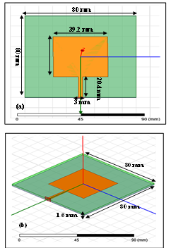 Figure 1: The basic geometry of the reference antenna
(a): front view and (b): side view
As expected, the simulated reflection coefficient S11 of the (RA), using HFSS Software, indicates that the (RA) operates at a single frequency 2.45 GHz. The simulated value of S11 parameter is
-17.02 dB. The bandwidth at -10 dB is 0.07 GHz. This result agrees well with the published measurement results in [15].
2.2 Proposed antenna structure
Admittedly, the goal of this paper is to achieve the shifting frequency exploiting the [2.45 – 3] GHz band because this part of the frequency spectrum is not exploitable by carrying out experimental measurements in [15]. To solve this problem, the proposed procedure for obtaining the frequency agility requires the integration of two varactor diodes on the square patch antenna. In order to insert the varactor diodes, the rectangular slots are etched on the radiating element and optimized using electromagnetic Ansoft HFSS software. The antenna design and performance parameters are discussed in the following sections. The proposed antenna structures are presented in Fig 2.
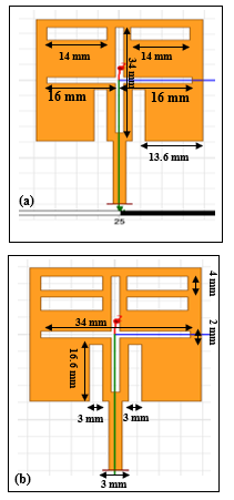 Figure 2: Proposed antenna structures with different dimensions of etched slots (a) patch with 2 slots in the superior part, (b) patch with 4 slots in the superior part
In order to study the mechanism of insulation and electromagnetic radiation in the two proposed structures, an analysis of surface currents is used. This analysis will enable us to adopt one of the two proposed structures as an investigation structure. It also makes it possible to locate the places of integration of the active elements in the adopted antenna structure. The current distributions on the radiated electric patches of the proposed structures are depicted in Fig 3. Note that, the current distributions in both proposed structures are presented at 2.45 GHz.
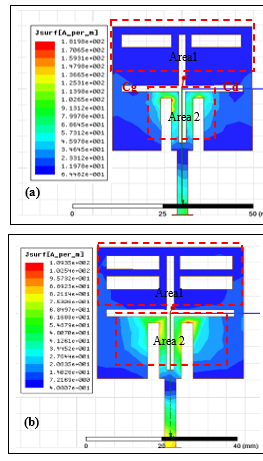 Figure 3: Current distributions on the radiated electric patches of the proposed structures at 2.45 GHz:
(a) Current distributions of the patch with 2 slots,
(b) Current distributions of the patch with 4 slots.
As presented in Fig 3a and Fig 3b, two areas can be identified on each structure. These areas are indicated in both Figs by two red dashed rectangles. On the one hand, the areas indicated by (area 2) are characterized by a very high distribution of excitation currents and they contribute to the radiation of the antenna. However, it is also clear that the areas indicated by (area 1) do not contain excitation currents. These areas are used for the integration of the varicap diodes. On the other hand, by comparing the amplitudes of the current distributions on the radiated electric element patches of the two proposed structures, it is clear that the amplitude of the current distributions in Fig (3a) is higher than that in Fig (3b). This comparison justifies the choice of the structure shown in figure (3a) as the investigated structure.
3. Results and Discussion
3.1 Integration of varactor diodes in pair (i.e: Cd=Cg)
Since the varactor diode cannot be applied in the HFSS software, it is replaced by a lumped capacitor. Two varactor diodes are embedded on the radiated electric patch. The locations of the integrated active elements are optimized using HFSS. The positions are the two horizontal rectangles of dimensions (16 × 2) mm2, as indicated in Fig 3a. The right varactor diode is noted by Cd, while the left diode is noted by Cg. By electronically controlling the biasing voltages distribution across the varactor loaded line, a reconfigurable frequency can be obtained. In order to show the achieved frequencies using the proposed antenna structure, the diagrams of reflection coefficient S11 versus frequency for different values of the capacitances (same values of varactor diodes i.e. Cd=Cg) are presented in Fig 4.
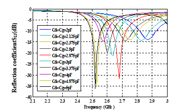 Figure 4: S11 versus frequency for different values of
varactor diodes (i.e: Cd=Cg)
The different values of the capacitances create different electrical lengths [16]. As a result, different resonance frequencies are obtained for the proposed antenna, which goes in line with the purpose of this article. As shown in Fig 4, frequency reconfigurability is achieved between 2.52GHz and 2.88 GHz. Many resonance frequencies with different bandwidths are achieved by changing the values of the pair varactor diodes i.e. (Cd=Cg). Table 1 displays the different achieved resonance frequencies as functions of the integrated capacitance values.
In this configuration, (i.e. the capacitances change the values in pair), the frequency agility is ensured in the frequency band
[2.52 – 2.88] GHz and the reflection coefficient reach (-36 dB) for the operated frequency 2.52 GHz. It is also important to note that the evolution of the resonance frequency is inversely proportional to the values of the integrated diodes. For an experimental point of view, the integrated varactor diodes on the radiant element should be fed with the same reverse bias voltage.
Table 1: Different achieved resonant frequencies as functions of the integrated capacitance values
| Capacitance value (pF) |
Resonance Frequency (GHz) | Reflection coefficient S11(dB) | Bandwidth (GHz) (-10dB) |
| Cd=Cg=5 | 2.52 | -36.01 | 0.07 |
| Cd=Cg=4.875 | 2.53 | -35.42 | 0.07 |
| Cd=Cg=4 | 3.57 | -14.89 | 0.07 |
| Cd=Cg=3.375 | 2.6 | -19.99 | 0.08 |
| Cd=Cg=3 | 2.64 | -21.21 | 0.08 |
| Cd=Cg=2.875 | 2.68 | -31.79 | 0.08 |
| Cd=Cg=2.5 | 2.72 | -14.49 | 0.11 |
| Cd=Cg=2.375 | 2.75 | -14.12 | 0.11 |
| Cd=Cg=2.125 | 2.83 | -14.45 | 0.11 |
| Cd=Cg=2 | 2.88 | -13.81 | 0.11 |
3.2 Varactor diodes Effect on the antenna parameters
3.2.1 Effect on the radiation pattern
In an attempt to evaluate the effects of the integrated elements on the radiation pattern, the gain and the radiation efficiency, the evolutions of these parameters as functions of the integrated capacitance values are presented. For this purpose, the radiation patterns of the proposed antenna structure in the E(φ=0°) and H(θ=90°) planes are simulated using HFSS software. The simulated radiation patterns at some achieved resonance frequency are shown in Fig 5a and Fig 5b.
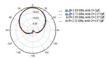 Figure 5 a : Simulated 2D radiation pattern E-Plan (φ = 0°) at resonance frequencies of the proposed antenna
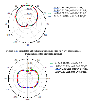 Figure 5 b: 2D radiation pattern on H-Plan (θ = 90°) at resonance frequencies of the proposed antenna
According to Figures 5a and 5b, it is clear that the diagrams in both planes E (φ = 0 °) and H (θ = 90 °) are substantially identical. The radiation patterns in the two planes E and H show good stability despite the frequency agility achieved by the control of the integrated capacitance values.
3.2.2 Effect on the gain antenna
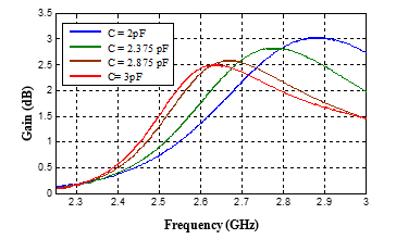 Figure 6: Gain (dB) as function of integrated capacitance value
Fig 6 shows the gain (dB) of the proposed antenna structure at various achieved operating frequencies by the values control of the integrated capacities.
As indicated in Fig 6, the proposed antenna has an acceptable gain. The maximum gain is 3.02 dB when the capacitance value is fixed at C=2pF with the resonance frequency F=2.88 GHz. It should be also noted that the gain value decreases as the integrated capacitance values increase. This increase is accompanied by a shift towards the resonance frequencies obtained close to 2.52 GHz.
3.2.3 Effect on the radiation efficiency
The radiation efficiency characteristics in (%) of the proposed antenna is calculated and illustrated in Fig 7.
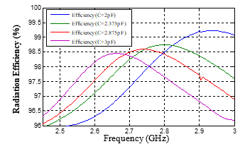 Figure 7: Radiation efficiency as function of integrated capacitance value
As depicted in Fig 7, the radiation efficiency of the proposed antenna resides within the range of 96 % and 99.25%. We also notice that when the capacitance value increases, the efficiency decreases. Note also that the radiation efficiency reaches its peak at each resonance frequency.
3.3 Integration of two varactor diodes with (Cd#Cg)
To shove the antenna to scan a large number of operating frequencies points, the values of the integrated varactor diodes are separately optimized (i.e. each diode may have a specific capacitance value). To this end, the simulated results of the reflection coefficient S11 as a function of frequency and capacitance values are presented in Fig 8.
|
Reflection coefficientS11(dB)
|
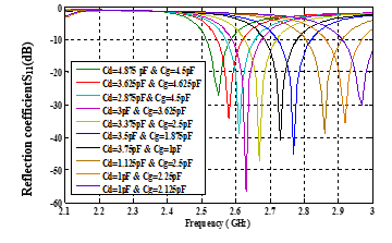 Figure 8: S11 versus frequency for different values of capacitance values
Fig 8 presents a good use of the frequency band which is ensured by varying separately the values of the integrated diodes. For the 2.63 GHz frequency, the S11can reach a value of -56.04 dB. The obtained results show that the variation of the capacitance is more effective than the change of the physical size of the antenna. As indicated in Fig 8, each operated resonance frequency is associated with a specific capacitance value. To show the improvements assigned to the (RA), the simulated results (Table 2) of the proposed antenna are compared with the published measurements (Table 3) of the reference antenna [15]
Table 2: The achieved frequencies via simulation using proposed antenna
| Simulation Results | ||||
| Capacitance value (pF) | Resonance Freequency (GHz) |
Reflection coefficient S11 (dB) |
Bandwidth (GHz) (-10dB) |
|
| Cd = 4.875 | Cg = 4.5 | 2.55 | -27 | 0.072 |
| Cd = 3.625 | Cg = 4.625 | 2.58 | -34.38 | 0.076 |
| Cd = 2.875 | Cg = 4.5 | 2.61 | -38.72 | 0.086 |
| Cd = 3 | Cg = 3.625 | 2.63 | -56.04 | 0.087 |
| Cd = 3.375 | Cg = 2.5 | 2.67 | -47.37 | 0.1 |
| Cd = 3.5 | Cg = 1.875 | 2.73 | -40.48 | 0.097 |
| Cd = 3.75 | Cg = 1 | 2.77 | -45.07 | 0.1 |
| Cd = 1.125 | Cg = 2.5 | 2.86 | -38.81 | 0.107 |
| Cd = 1 | Cg = 2.25 | 2.92 | -35.63 | 0.106 |
| Cd = 1 | Cg = 2.125 | 2.971 | -29.3 | +0.1 |
Hence, the results demonstrate that the separated optimization of the integrated varactor diodes, using the proposed antenna structure, yields good frequency flexibility on the frequency band [2.5 – 3] GHz. In addition, by comparing the obtained simulated results to the measurement results using the (RA), as indicated in table 2 and 3, the achieved frequencies are higher than the operated single frequency of the (RA), which are not obtained by the measurement results in [15]. On the other hand, the bandwidths at -10 dB are larger than the measurement results. For an experimental purpose, it is necessary to feed each integrated varactor diode separately to obtain two different values of capacitances.
Table 3: Measurement Results of (RA) published in [15]
| Measurement Results of (RA) | |||
| Capacitance value (pF) | Resonance Freequency (GHz) |
Reflection coefficient S11 (dB) |
Bandwidth (GHz) (-10dB) |
| 20 | 0.51 | -42 | 0.05 |
| 9.6 | 0.75 | -35 | 0.05 |
| 5.2 | 0.97 | -16 | 0.05 |
| 3.1 | 1.17 | -12 | 0.03 |
| 1.7 | 1.51 | -10 | 0.025 |
| 1.3 | 1.7 | -11 | 0.025 |
| 0.9 | 2.4 | -12 | 0.05 |
To have the reliability of the obtained simulated results, we have compared them with references published in [16-19]. In this respect, Table 4 presents this comparison of the performances of our proposed antenna concerning the bandwidth, resonance frequency and reflection coefficient.
Table 4: Comparison of proposed antenna with published results
| Antenna Ref |
Bandwidth (%) |
Resonance Frequency (GHZ) | Reflection coefficient S11 (dB) |
| Antenna in [16] | 4 | 2.5- 2.6 | -15 |
| Antenna in [17] | 6.06 | 2.31 | -20 |
| Antenna in [18] | 5.58 | 2.15 – 2.36 | -20 |
| Antenna in [19] | 14.58 | 2.4 – 2.6 | -45 |
|
Antenna in this work |
28 | 2.5–3 | -56.04 |
According to Table 4, we deduce that our antenna design can have a large band that can reach up to 28% [2.4 – 3.] GHz (UHF band), with a resonance frequency that varies between 2.5 GHz and 3 GHz; whereas other published structures do not exceed 15%. The proposed antenna has an important reflection coefficient (-56.04 dB) especially at the resonance frequency
f = 2.63GHz as well as a large band compared to the published antennas. The proposed structure allows varying its resonance frequency from 2.5 GHz to 3 GHz by controlling the integrated capacitance values.
4. Conclusion
This article has presented an analysis of the frequency reconfigurable square patch antenna. The proposed antenna structure achieves the desired frequency agility by integrating two varactor diodes on the rectangular slots that have been etched on the radiant element patch. The proposed antenna design has been examined for frequency reconfigurability; therefore, its performances have found a satisfactory comparison with the published results. When the two integrated varactor diodes are separately optimized, the frequency shifting allows a powerful sweep of the [2.5 – 3] GHz band. This part of the spectrum is not exploitable by the reference antenna. This comparative study between our simulated results and the previously published results of the reference antenna will be completed in the next works by a real comparison between simulated and experimental results when we make a realization of the proposed structure.
- Christos, G., Christodoulou, Y., Steven, A., and Scott, R,: “Reconfigurable Antennas for Wireless and Space Applications,” Proceedings of the IEEE, 100, (7), pp 2250 – 2261. July 2012.
- Qin P., Weily R., Guo, Y., and Liang, C., “Polarization Reconfigurable U-slot patch Antenna,” IEEE Trans. Antennas and Propagation, 58, (10), pp 3383 – 3388, Octobre, 2010.
- Bin, L., Benito S., Edward A. , and John, B., :”A Frequency and Polarization Reconfigurable Circularly Polarized Antenna Using Active EBG Structure for Satellite Navigation,” IEEE Trans on Antennas and Propagation, ,63, (1),pp 33 – 40, January 2015.
- Qin, P., Guo, Y., Cai, E., Liang, C., :”A Reconfigurable Antenna with Frequency and Polarization Agility”, IEEE Antennas Wireless Propagation Letters, 10, pp 1373 – 1376, 2011.
- Nghia, N., Leonard, H., Christophe, F.,:”A Frequency and Polarization-Reconfigurable Stub-loaded Microstrip Patch Antenna” IEEE Trans. Antennas and Propagation, 63, (11), pp 5235-5240, 2015.
- Wei, L., Hang, W., “Polarization Reconfigurable Aperture-Fed Patch Antenna and Array, “ IEEE Access, April 2016, 4, pp 1510 – 1517.
- Jay, Y., Pei-yuan, Q., Shu-lin, C., Wei, L., Richard W. Ziolkowski1, “advances in reconfigurable antenna systems facilitated by innovative technologies,” IEEE, 6, pp 5780 – 5794, 2018.
- Chang, Y., Jea Hak K., Woo, J., Taejoon, P., Byungje, , Chang, W.,”Frequency-Reconfigurable Antenna for Broadband Airborne Applications,” IEEE Antennas and Wireless Propagation Letters, , 13, (23), pp 189 – 192 , January 2014.
- Shakhirul, S., Muzammil, J., Abdul Hafiizh, I., Muhammad K., Philip, N., Mohamad, K., Rahim, M., Thennarasan, S., Mohamed, N., Jais, M., Ping, J., “Textile Antenna With Simultaneous Frequency and Polarization Reconfiguration for WBAN,” IEEE Access, 6, pp 7350 – 7358, March 2018.
- Rocktotpal, B and Nidhi, S.,”A Frequency Reconfigurable Meandered Slot Cut Rectangular Patch Antenna Using PIN Diodes Progress In Electromagnetics Research C,”77, pp 81–89, 2017.
- Yamagajo, T, Koga, Y., “Frequency reconfigurable antenna with MEMS switches for mobile terminals,” IEEE-APS Topical Conference on Antennas and Propagation in Wireless Communications, October, 2011.
- Liang, J., Yang, H., “Varactor Loaded Tunable Printed PIFA Progress In Electromagnetics Research B,” 15, pp, 113–131, 2009.
- Seung-Bok, B., et al, “Reconfigurable Ground-Slotted Patch Antenna Using PIN Diode Switching;” ETRI Journal, 29, (6), pp, 832 -834, December 2007.
- Rouissi, I., Floc’h, J., Trabelsi, H., “Design of Frequency Reconfigurable Multiband Meander Antenna Using Varactor Diode for Wireless Communication, International Journal of Advanced Computer Science and Applications,” 8, (3), pp, 159 – 164, 2017.
- I Rouissi, I.,. Floc’h, J., Rmili, H., Trabelsi, H., “Design of a frequency reconfigurable patch antenna using capacitive loading and varactor diode, 9th European Conference on Antennas and Propagation,” EuCAP 2015.
- Sung Woo Lee, Youngje Sung, “A Polarization Diversity Patch Antenna with a Reconfigurable Feeding Network”, Journal of Electromagnetic Engineering and Science, vol. 15, no. 2, 115~119, apr. 2015.
- Seung-Bok Byun, Jeong-An Lee, Jong-Hyuk Lim, and Tae-Yeoul Yun, “Reconfigurable Ground-Slotted Patch Antenna Using PIN Diode Switching”, ETRI Journal, Volume 29, Number 6, December 2007.
- Suresh Kumar M and Yogesh Kumar Choukiker, “Study of Frequency and Polarization Reconfigurable on Square Patch Antenna “, International Journal of Engineering and Manufacturing Science. Volume 8, Number 1 pp. 145-149, 2018.
- Mustafa Murat Bilgiç and Korkut YeLin, “Polarization Reconfigurable Patch Antennafor Wireless Sensor Network Applications”, International Journal of Distributed Sensor Networks, 2013.