A New Wire Optimization Approach for Power Reduction in Advanced Technology Nodes
 , Mohamed Chentouf 2, Mohammed Darmi 1, Rachid Elgouri 3, Nabil Hmina 1
Adv. Sci. Technol. Eng. Syst. J. 4(6), 140–146 (2019);
 DOI: 10.25046/aj040617
In advanced technologies nodes, starting from 28 nm to 7 nm and below, the power consumed of integrated circuits (ICs) becomes a big concern. Consequently, actual electronic design automation (EDA) tools are facing many challenges to have low power, reduced area and keep having required performance. To reach required success criteria, and because each picosecond and each picowatt counts, continuous development of new optimization technics is necessary. In this paper, we put to the experiment and analysis a new technic to reduce IC consumed power by optimizing its interconnections (nets). We propose an optimal algorithm and enhance it for a better compromise between having less consumed power and keep having a good design rout-ability. The new wire optimization technic based on an optimal choice of target nets for optimization: which is the list of nets consuming more than 80% of the total power in the interconnection without exceeding 30% of the total number of nets. Experiments on 14 test cases show an average total power saving of 5% on both dynamic and total power.
1. Introduction
Modern system on chip (SoC) and network on chip (NoC) circuits are known by the integration of complex interconnect IP which brings more difficulties for the timing closure especially with the 16 nm technology node (and below) [1]. In parallel with the circuit performance, new technology nodes allowed a very high transistors’ integration to have more functionalities inside smaller die area [2], which brings many manufacturing challenges before having production circuits. On the other hand, modern designs are power-constrained (e.g., IoT, Automotive, Mobile) [3, 4]. Thus, electronic design automation (EDA) tools should have all necessary functionalities for a good compromise between required circuit performances, manufacturing, and power consumption.
In advanced technology nodes, wire capacitance has become a key challenge to design closure, and this problem only worsens with each successive manufacturing process mainly due to the minimum spacing between adjacent wires [5, 6]. Today, a physical implementation flow for the digital circuit should be able to play with multiple scenarios during routing to find the best compromise between timing, power, and rout-ability. [7] Details the importance of interconnect optimization and how its optimization is playing a pillar role in chip performance. Also, [8, 9] Present more routing closure challenges.
Related to the power optimization, at the physical implementation, many technics are used targeting both leakage and dynamic power. [10, 11] Gives some technics to reduce power on the cells’ element. [12, 13] present new technics for power optimization on the design network. [14, 15] focus more on the technology ways to decrease total consumed power in the design.
This work introduces a new technique for power optimization during the physical implementation of an IC by optimizing the wire capacitance of its power critical interconnections (nets). We then propose a new solution that directly improves upon the original solution [16] construction by proposing an enhancement of the procedure that gets target nets for optimization. The new solution helps for having good route congestion overflow while keeping the same power reduction gain. The solution approach achieves improvement for both objectives, having a maximum power gain by simple nets re-routing, and reduce the overflow for better design rout-ability.
Experimental results on 14 test-cases made with most advanced technologies nodes (28, 20, 16&7 nm) demonstrate that this technique achieves an additional average of 5% on total power by targeting nets consuming more than 80% of the power.
This paper makes the following contributions:
- Starting with the final result from paper [16], in this paper, we propose an enhanced procedure that gets fewer data nets as a target for optimization.
- The enhanced solution helps on having acceptable routing congestion for better routing capability and, at the same time, keep having the same good power reduction gain of 5% in the average.
- Proves the benefit of this transform on power reduction on data nets by experimenting with the new flow on 14 real designs made with the most advanced technology nodes 28, 20, 16 and 7 nm.
The remainder of this paper is organized as follows. Section 2 presents the power trend on a modern integrated circuit and briefly, review the results achieved in paper [16]. Section 3 presents the enhanced solution that gets fewer targets for better routing congestion overflow as a wire promotion power-aware method. Section 4 reports our experimental results, and Section 5 concludes the paper.
2. Power in digital ICs at physical implementation stage
2.1. Power calculation and the trend in advanced technology nodes
Equations (1), (2) and (3) summaries how the IC power can be calculated: [17-19]
 Where:
are rise and fall energy;
toggle_rate is number of toggles per time-unit;
is total wire capacitance;
V is the power supply voltage
During IC physical implementation, only a few parameters could be optimized; for example: reduce the wire capacitance by making the interconnection wire-length shorter or by spreading. Swap cells with high internal or leakage power with lower cells’ power.
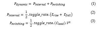
In advanced nodes 28 nm and below, static power consumption represents less than 10%, on average, of the total power consumed by an IC. The dynamic circuit power is composed of the internal power that represents 20% to 30% and the switching power representing 70% to 80% of the overall consumption of a circuit [20, 21]. These numbers are proved in test-cases we are using for this paper: Table 1, shows a summary of their main characteristics. Figure 1, shows their average static and dynamic power repartition. Figure 2 shows the different average power components repartition. It is evident to see that by targeting all the “Data nets”, we are targeting more than 50% of the total power for optimization.
Table 1: Design Specifications
| Designs | Number of instances |
Number of nets |
Physical area (µm²) |
Technology (nm) |
| Design#1 | 535815 | 566853 | 407658 | 20 |
| Design#2 | 557185 | 588503 | 470164 | 20 |
| Design#3 | 905670 | 1268272 | 1072040 | 7 |
| Design#4 | 137950 | 221084 | 46975.9 | 7 |
| Design#5 | 477969 | 546368 | 236706 | 16 |
| Design#6 | 3695650 | 8402104 | 5949560 | 28 |
| Design#7 | 637450 | 642466 | 392697 | 16 |
| Design#8 | 779966 | 777869 | 475353 | 16 |
| Design#9 | 2780115 | 5315732 | 4468680 | 28 |
| Design#10 | 2288833 | 3179391 | 2982620 | 28 |
| Design#11 | 3362065 | 4974698 | 4752870 | 28 |
| Design#12 | 885391 | 1162839 | 1608120 | 28 |
| Design#13 | 798317 | 1042158 | 1916400 | 28 |
| Design#14 | 587529 | 1286854 | 5309480 | 16 |
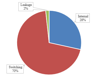 Figure 1: Static (Leakage) and dynamic (Internal + Switching) Power reparation
2.2. Wire optimization to reduce Net power
In our previous research [16], we presented a wire optimization technique for power saving on the interconnection at the physical implementation phase of an IC. At this stage, the circuit voltage and the TR are fixed by the circuit function, and we can’t do anything to reduce them. The remaining parameter is the interconnection capacitance. This represents an opportunity for significant power saving using routing transforms.
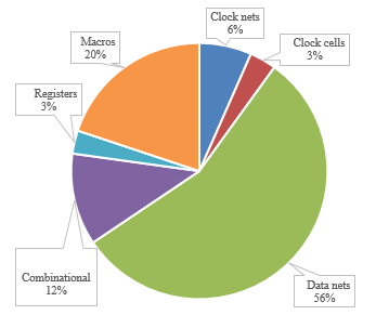 Figure 2: Multiple IC power components repartition
The complexity of capacitance variations makes it nearly impossible for the human mind to determine which combination of layers and via structures to use for a given net in order to obtain the less possible power consumption and keeping an acceptable timing and good routing. This can be achieved through layer promotion of power critical nets, coupled with a carefully set of double-spacing non-default rules (NDRs). Enabling the routing engines to efficiently trade-off timing quality of results (QoRs) and congestion.
We have used Mentor Graphics Nitro-SoC™ [22] tool and the correspondent place and route full flow [23, 24] to implement test-cases used during this study.
As a review of results achieved in our previous work, reference [16] proves the following results:
- 40% of data nets are consuming 92.6% of the total power as shown in Figure 3.
- Start having a signifying power reduction up to 20% on power consumed by data nets when the number of target nets exceeds 40% of the total number of data nets: Figure 4.
- Total power reduction percentage approaching 7 %: Figure 5.
- A good compromise between the power saving and the timing/congestion was achieved by taking the cases 40% and 30% of total data nets number as a target for power optimization.
3. Results and analysis
3.1. Algorithm enhancement for better congestion overflow
In the previous section, we have introduced our research by presenting a reminder of results achieved in previous work [16]. Experiment on one test-case shows an important total power saving gain exceeding 5% by targeting 30% of data nets for optimization.
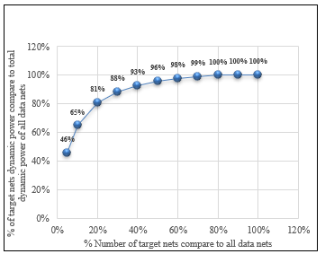 Figure 3: Data Nets power repartition
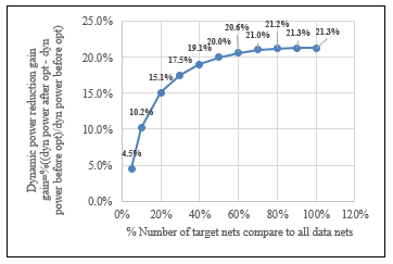 Figure 4: Dynamic power gain on data Nets
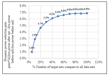 Figure 5: Total power gain on entire design
In this section, we will apply this optimal solution to multiple designs made with different technologies nodes. The goal is to see if this solution is robust enough for production usage.
For a good comparison, we are applying the wire optimization for power reduction on an optimized post-clock-tree-synthesis (post_CTS) database (db). The baseline run that produces initial post-CTS db is a full place and route flow power-driven [23, 24]. Thus, with our solution, we will be able to see the exact power gain after using existing power optimization transforms. Experiments are done on 14 test cases made with advanced technologies nodes 28 nm, 20 nm, 16 nm, and 7 nm. Their main characteristics are summarized in table 1:
Algorithm#2, shows the automatic incremental optimization flow for power reduction:
| Algorithm # 2: Automatic incremental flow |
| 1. set designs_list = (Design#1, Design#2, Design#3, Design#4, Design#5, Design#6, Design#7, Design#8, Design#9, Design#10, Design#11, Design#12, Design#13, Design#14) |
| 2. For design ($designs_list)
a. Read baseline saved Post-CTS Database |
| b. Report & save Initial QoR (Timing, Power, and Congestion)
c. Create double spacing NDRs on all used layers for routing. |
| d. Get 30% of data nets with highest power consumption (see next section for more details: Procedure#1)
e. Apply NDRs on Target_Nets list |
| f. Run the native global route |
| g. Run one optimization pass for Timing recovery |
| h. Run the native global route |
| i. Report QoR (Timing, Power, and Congestion) |
| 3. END for |
The section below describes the main procedure that gets target nets for optimization. Its objective is to get 30% of data nets having high dynamic power.
| Procedure # 1: Get target nets: 30% of data nets with the highest power consumption |
| 1. Filter data nets from all nets (data_nets) |
| 2. For each data_net ($data_nets) |
| a. Get its dynamic power and save it in a table |
| b. Save the data_net and its dynamic power |
| 3. END for |
| 4. Rank nets in order of power consumption. |
| 5. Return first 30% of data_nets |
For all trials, the target nets are 30% of data nets that have the highest power consumption, while in some test cases we see that by targeting only 20% of data nets we are targeting more than 80% of the total power consumed in the interconnection. This remark conducts us to an optimal solution by targeting a dynamic list of nets consuming more than 80% of the total power.
The new procedure that gets target nets for optimization is described below:
| Procedure # 2: Get target nets: nets consuming > 80% of the total power in the interconnection |
| 1. Filter data nets from all nets (data_nets)
2. Get the total dynamic power of all $data_nets (data_nets_power) |
| 3. For each data_net ($data_nets) |
| a. Get its dynamic power and save it in a table |
| b. Save the data_net and its dynamic power |
| 4. END for |
| 5. Rank nets in order of power consumption. |
| 6. Return the first list of nets consuming >80% of total data_nets_power |
Table 2, shows a comparison between cases performed by using procedure#1 and procedure#2. We notice an important “Overflow” reduction in almost all test-cases.
The high overflow reduction is happening on designs having a low activity such as “Design#1, Design#2, Design#3 and Design#4”. The low overflow is coming especially from the important reduction of target nets from 30% to 2% for Design#1, 3% for Design#2, and 4% for Design#3. For these test-cases the low target nets percentage is sufficient to have good power reductions achieving -17.5%, -16.3%, -7.6% and -7.5% respectively.
For other designs, Design#5 to Design#13, by targeting 20% instead of 30% of data nets, we achieve almost the same power gain lower congestion overflow. Finally, one test-case “Design#14” ends with the same target nets percentage of 30% and a power gain of -19%.
3.2. Power gain on overall designs
In the previous section, we notice an important reduction of the number of target nets considered for optimization with proc#2 compare to proc#1. Fewer target nets number with almost the same or better power gain is helping for a fast run time accompanied by a better rout-ability. All of that conduct to an optimal solution, which is to target the number of nets consuming more than 80% of the total net’s power with a maximum of 30% of the total nets number.
Table 3, presents the dynamic and total power gain for each design using the optimal solution. An average of 5% power reduction obtained in both dynamic and total power.
Table 2: Comparison between Procedure#1 and Procedure#2.
Target nets power gain = %( nets power after optimization- nets power before optimization)/ nets power before optimization
|
Before Optimization |
After Optimization | |||||||||
| Designs | Total number of nets |
Number of target nets |
% of target nets (%) |
Total nets power (mW) |
Target nets power (mW) |
% power of target nets (%) |
Overflow | Target nets power (mW) |
Target nets power gain (%) |
|
| Design#1 | Proc#1 | 483171 | 144951 | 30.0% | 1.0423 | 1.0423 | 100.0% | 3.41 | 0.8752 | -16.0% |
| Proc#2 | 483171 | 9663 | 2.0% | 1.0423 | 0.8578 | 82.3% | 1.10 | 0.7079 | -17.5% | |
| Design#2 | Proc#1 | 501314 | 150394 | 30.0% | 1.1548 | 1.1548 | 100.0% | 3.80 | 0.9781 | -15.3% |
| Proc#2 | 501314 | 15039 | 3.0% | 1.1548 | 0.9812 | 85.0% | 1.69 | 0.8209 | -16.3% | |
| Design#3 | Proc#1 | 878226 | 263468 | 30.0% | 41.998 | 41.8647 | 99.7% | 0.23 | 38.7659 | -7.4% |
| Proc#2 | 878226 | 35129 | 4.0% | 41.998 | 34.7165 | 82.7% | 0.15 | 32.0757 | -7.6% | |
| Design#4 | Proc#1 | 147116 | 44135 | 30.0% | 15.435581 | 15.435581 | 100.0% | 0.40 | 14.312023 | -7.3% |
| Proc#2 | 147116 | 5885 | 4.0% | 15.435581 | 15.435581 | 100.0% | 0.05 | 14.270356 | -7.5% | |
| Design#5 | Proc#1 | 433469 | 130041 | 30.0% | 102.6567 | 96.0036 | 93.5% | 4.46 | 70.924 | -26.1% |
| Proc#2 | 433469 | 86694 | 20.0% | 102.6567 | 90.8166 | 88.5% | 4.08 | 66.463 | -26.8% | |
| Design#6 | Proc#1 | 3618017 | 1085405 | 30.0% | 892.1152 | 821.1902 | 92.0% | 7.56 | 712.3573 | -13.3% |
| Proc#2 | 3618017 | 723603 | 20.0% | 892.1152 | 780.1937 | 87.5% | 7.13 | 674.5511 | -13.5% | |
| Design#7 | Proc#1 | 636971 | 191091 | 30.0% | 53.3274 | 50.7283 | 95.1% | 2.39 | 39.7819 | -21.6% |
| Proc#2 | 636971 | 127394 | 20.0% | 53.3274 | 48.4197 | 90.8% | 2.15 | 37.6407 | -22.3% | |
| Design#8 | Proc#1 | 770303 | 231091 | 30.0% | 57.9306 | 55.0936 | 95.1% | 1.75 | 41.678 | -24.4% |
| Proc#2 | 770303 | 154061 | 20.0% | 57.9306 | 52.2459 | 90.2% | 1.49 | 39.1292 | -25.1% | |
| Design#9 | Proc#1 | 2436751 | 731025 | 30.0% | 939.3153 | 875.8495 | 93.2% | 4.75 | 726.5736 | -17.0% |
| Proc#2 | 2436751 | 487350 | 20.0% | 939.3153 | 831.0609 | 88.5% | 4.50 | 688.0895 | -17.2% | |
| Design#10 | Proc#1 | 2020267 | 606080 | 30.0% | 1479.458 | 1377.5008 | 93.1% | 8.69 | 1150.6352 | -16.5% |
| Proc#2 | 2020267 | 404053 | 20.0% | 1479.458 | 1297.9898 | 87.7% | 8.19 | 1082.2901 | -16.6% | |
| Design#11 | Proc#1 | 3100457 | 930137 | 30.0% | 2615.8898 | 2411.9914 | 92.2% | 8.11 | 1991.3135 | -17.4% |
| Proc#2 | 3100457 | 620091 | 20.0% | 2615.8898 | 2266.4228 | 86.6% | 7.70 | 1865.8817 | -17.7% | |
| Design#12 | Proc#1 | 822186 | 246656 | 30.0% | 435.9402 | 411.998 | 94.5% | 7.83 | 346.8801 | -15.8% |
| Proc#2 | 822186 | 164437 | 20.0% | 435.9402 | 394.3237 | 90.5% | 7.57 | 332.0825 | -15.8% | |
| Design#13 | Proc#1 | 745762 | 223729 | 30.0% | 378.2664 | 338.9859 | 89.6% | 4.86 | 274.266 | -19.1% |
| Proc#2 | 745762 | 149152 | 20.0% | 378.2664 | 313.018 | 82.8% | 4.55 | 253.8826 | -18.9% | |
| Design#14 | Proc#1 | 466631 | 139989 | 30.0% | 903.8741 | 790.2763 | 87.4% | 6.30 | 640.3705 | -19.0% |
| Proc#2 | 466631 | 139989 | 30.0% | 903.8741 | 790.2763 | 87.4% | 6.30 | 640.3705 | -19.0% | |
Table 3: Dynamic and total power gain
power gain = %(power after optimization- power before optimization)/ power before optimization
| Before Optimization | After Optimization | |||||
| Designs | Dynamic Power (mW) | Total power (mW) |
Dynamic Power (mW) | Total power (mW) |
Dynamic power gain (%) | Total power gain (%) |
| Design#1 | 8.0476 | 8.0711 | 7.9125 | 7.9359 | -2% | -2% |
| Design#2 | 8.7976 | 8.9791 | 8.6429 | 8.8298 | -2% | -2% |
| Design#3 | 149.3188 | 152.1707 | 147.3411 | 150.1936 | -1% | -1% |
| Design#4 | 113.042473 | 113.31836 | 111.774694 | 112.050549 | -1% | -1% |
| Design#5 | 330.4627 | 330.8185 | 307.2876 | 307.6482 | -7% | -7% |
| Design#6 | 2658.979 | 2659.736 | 2563.1845 | 2563.9415 | -4% | -4% |
| Design#7 | 198.2466 | 198.3225 | 187.7011 | 187.7769 | -5% | -5% |
| Design#8 | 218.2062 | 218.3048 | 205.2356 | 205.334 | -6% | -6% |
| Design#9 | 2018.207 | 2126.9193 | 1872.6143 | 1981.4807 | -7% | -7% |
| Design#10 | 2964.9741 | 3043.4681 | 2748.532 | 2830.5278 | -7% | -7% |
| Design#11 | 4141.0681 | 4245.7608 | 3735.9251 | 3840.9783 | -10% | -10% |
| Design#12 | 894.2836 | 894.3742 | 833.1615 | 833.2521 | -7% | -7% |
| Design#13 | 702.7373 | 702.8631 | 643.1108 | 643.2364 | -8% | -8% |
| Design#14 | 2693.7224 | 2694.3472 | 2595.0319 | 2595.6581 | -4% | -4% |
| Average | -5.18% | -5.10% | ||||
4. Conclusion
In this paper, we present a new wire optimization technique for power reduction during IC physical implementation phase. The main outcome is the optimal choice of target nets for optimization, which is the list of power critical nets consuming more than 80% of total power in the interconnection without exceeding the number of nets of 30% of the total nets. Experiment on 14 test-cases made with advanced technologies nodes shows an important power reduction and, at the same time, keeps having good design rout-ability.
The technique leads to an important dynamic power improvement through a simple critical Nets re-routing. The power on all data Nets reduced up to 20% and the average total power reduction in all test-cases by 5%.
Conflict of Interest
The authors declare no conflict of interest.
Acknowledgment
This research supported by Mentor Graphics Corporation. We thank Dr. Hazem El Tahawy (Mentor Graphics, Managing Director MENA Region) for initiating and supporting this work.
- K. C. Janac, “Interconnect Physical Optimization,” Proceedings of the 2018 International Symposium on Physical Design – ISPD 18, 2018.
- D. J. Radack and J. C. Zolper, “A Future of Integrated Electronics: Moving Off the Roadmap,” in Proceedings of the IEEE, vol. 96, no. 2, pp. 198-200, Feb. 2008. doi: 10.1109/JPROC.2007.911049.
- D. Flynn, R. Aitken, A. Gibbons, K. Shi, Low power methodology manual: for system-on-chip design, 2ed. ed., Springer, 2007, p13.
- I. Lee and K. Lee, “The Internet of Things (IoT): Applications, investments, and challenges for enterprises,” Business Horizons, vol. 58, no. 4, pp. 431–440, 2015.
- C. J. Alpert, W.-K. Chow, K. Han, A. B. Kahng, Z. Li, D. Liu, and S. Venkatesh, “Prim-Dijkstra Revisited,” Proceedings of the 2018 International Symposium on Physical Design – ISPD 18, 2018.
- ITRS 2015 Edition Report-Interconnect, https://www.semiconductors.org/wp-content/uploads/2018/06/6_2015-ITRS-2.0_Interconnect.pdf, 2015.
- J. Hu, Y. Zhou, Y. Wei, S. Quay, L. Reddy, G. Tellez, and G.-J. Nam, “Interconnect Optimization Considering Multiple Critical Paths,” Proceedings of the 2018 International Symposium on Physical Design – ISPD 18, 2018.
- S. Mantik, G. Posser, W.-K. Chow, Y. Ding, and W.-H. Liu, “ISPD 2018 Initial Detailed Routing Contest and Benchmarks,” Proceedings of the 2018 International Symposium on Physical Design – ISPD 18, 2018.
- X. Qiu and M. Marek-Sadowska, “Routing Challenges for Designs With Super High Pin Density,” IEEE Transactions on Computer-Aided Design of Integrated Circuits and Systems, vol. 32, no. 9, pp. 1357–1368, 2013.
- L. Cherif, M. Chentouf, J. Benallal, M. Darmi, R. Elgouri and N. Hmina, “Usage and impact of multi-bit flip-flops low power methodology on physical implementation,” 2018 4th International Conference on Optimization and Applications (ICOA), Mohammedia, Morocco, 2018, pp. 1-5. doi: 10.1109/ICOA.2018.8370498.
- M. Rahman, R. Afonso, H. Tennakoon and C. Sechen, “Design automation tools and libraries for low power digital design,” 2010 IEEE Dallas Circuits and Systems Workshop, Richardson, TX, 2010, pp. 1-4.
- M. Chentouf, L. Cherif and Z. El Abidine Alaoui Ismaili, “Power-aware clock routing in 7nm designs,” 2018 4th International Conference on Optimization and Applications (ICOA), Mohammedia, Morocco, 2018, pp. 1-6. doi: 10.1109/ICOA.2018.8370505.
- L. Cherif, J. Benallal, M. Darmi, M. Chentouf, R. Elgouri, and N. Hmina, “ASIC Physical Design Flow: Power Saving Opportunities on Interconnection Components,” Lecture Notes in Electrical Engineering Proceedings of the 1st International Conference on Electronic Engineering and Renewable Energy, pp. 258–265, Feb. 2018.
- L. Cherif, M. Darmi, J. Benallal, R. Elgouri, and N. Hmina, “Last-Mile Post-Route Power Optimization in Integrated Circuit Conception,” International Journal of Engineering & Technology, 7(4.16), 102-105. doi:http://dx.doi.org/10.14419/ijet.v7i4.16.21788.
- G. J. Y. Lin, C. B. Hsu and J. B. Kuo, “Critical-path aware power consumption optimization methodology (CAPCOM) using mixed-VTH cells for low-power SOC designs,” 2014 IEEE International Symposium on Circuits and Systems (ISCAS), Melbourne VIC, 2014, pp. 1740-1743.
- L. Cherif, M. Chentouf, J. Benallal, M. Darmi, R. Elgouri and N. Hmina, “Layer Optimization for Power Reduction in Integrated Circuits,” 2018 IEEE 5th International Congress on Information Science and Technology (CiSt), Marrakech, Morocco, 2018, pp. 625-629. doi: 10.1109/CIST.2018.8596605.
- J. M. Rabaey, A. P. Chandrakasan, and B. Nikolic, Digital Integrated Circuits: A Design Perspective, 2nd ed., Prentice Hall Electronics and VLSI Series, Upper Saddle River, NJ: Pearson Education, 2003.
- K. Y. Gary, Practical Low Power Digital Vlsi Design. Springer Verlag, 2012. doi:10.1007/978-1-4615-6065-4.
- M. S. Elrabaa, I. S. Abu-Khater, and M. I. Elmasry, Advanced low-power digital circuit techniques. Boston: Kluwer Academic Publishers, 1997.
- J-G. Cousin, D. Chillet and O. Sentieys, “Power Estimation and Optimisation for ASIPs”, Submited to 1997 International Symposium on Low-Power Design, Mont. CA, Aug. 1997.
- E. Macii, “High Level Design and Optimization for Low Power”, NATO Advance Study : Low Power in Deep Submicron Electronics, Aug 1996.
- Nitro-SoC™ Software Version 2018.1, December 2018.
- Nitro-SoC™ “User’s Manual”, Software Version 2018, December 2018.
- Nitro-SoC™ “Advanced Design Flows Guide”, Software Version 2018, December 2018.