
Design and Simulation of a Doppler-Radar RF Front-End Transceiver
Volume 4, Issue 5, Page No 250-257, 2019
Author’s Name: Mohamed Elhefnawya)
View Affiliations
Department of Electrical Engineering, Faculty of Engineering, October 6 University, 12564, Egypt
a)Author to whom correspondence should be addressed. E-mail: mmmelhefnawy.eng@o6u.edu.eg
Adv. Sci. Technol. Eng. Syst. J. 4(5), 250-257 (2019); ![]() DOI: 10.25046/aj040531
DOI: 10.25046/aj040531
Keywords: RF front-end, Microwave components, Electromagnetic simulation tools

Export Citations
This paper presents the use of Electromagnetic simulation tools such as ADS and CST in order to practice designing the RF front-end transceiver for a continuous-wave radar. Teaching the microwave engineering course based on the conventional education methods results in students who may not be able to apply their theoretical knowledge to design the microwave components. This work introduces a project-based education which is expected to guide the undergraduate students toward the design and simulation of the most important active and passive microwave components such as oscillator, power amplifier, Cantenna, low noise amplifier, mixer, filter and power divider. This project can be added to the curriculum of the microwave engineering course to achieve a balance between the theoretical and practical knowledge.
Received: 27 July 2019, Accepted: 20 September 2019, Published Online: 08 October 2019
1. Introduction
The fundamentals of designing and simulating many microwave components are overviewed in this paper. The microwave engineering course curriculum needs to be modified in order to prepare the undergraduate students to meet the industry requirements [1]. The RF front-end transceiver for a continuous-wave radar has been developed using Advanced Design System (ADS) and Computer Simulation Technology (CST) tools. The RF front-end transceiver is a perfect platform for the undergraduate students to understand the design and simulation of microwave components. This paper presents an overview about the operation and structure of the Doppler radar; then the design and simulation of each microwave component are introduced; finally, the whole RF front-end transceiver for a continuous-wave radar is simulated using ADS.
2. Operation and Structure of a Doppler Radar
The Doppler radar transmits a continuous-wave at a specific frequency to an object; the frequency of the received reflected wave from the moving object is shifted due to Doppler effect. The velocity of the moving object can be calculated based on the relationship between the velocity and the Doppler frequency. Figure 1 shows the block diagram of the proposed RF front-end transceiver for a continuous-wave radar.
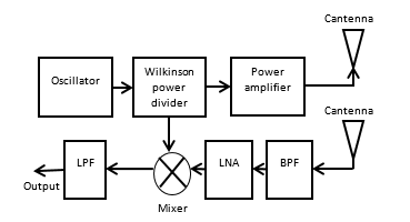 Figure 1: Block diagram of a Doppler-Radar RF Front-End Transceiver
There are two different Cantennas, one of them is used for transmitting the continuous-wave while the reflected wave is received by the other Cantenna. A power amplifier is used to increase the coverage area. The continuous wave is generated by a 10 GHz local oscillator. The Wilkinson power divider is used to equally divide the power of the oscillator between the power amplifier and the mixer. The reflected wave is received by the receiving Cantenna, and then it is filtered by a microstrip coupled line band pass filter (BPF) and amplified by a low noise amplifier (LNA). The output from LNA is applied to the microwave single balanced mixer. The mixer generates the Doppler frequency in addition to the other harmonics. The low pass filter (LPF) is implemented to remove the harmonics and pass the Doppler frequency.
3. Design and Simulation of Microwave Components
The microwave components of RF front-end transceiver for a continuous-wave radar are designed and simulated using ADS; also, these microwave components are made from microstrip lines with default substrate properties, except the metal Cantenna which is designed and simulated using CST.
3.1. Design and Simulation of 10 GHz Oscillator
The two-port transistor oscillator consists of the resonant circuit and the active circuit. The active circuit is connected with the resonant circuit to provide the required negative resistance that can cancel out the resistance of the resonant circuit; so that the resonant frequency with no damping can be generated. The design procedures of the proposed two-port oscillator are started by selecting a transistor (ATF-13786) which has a high degree of instability, then performing the stability checks using the output stability circles in ADS to find the unstable region on the Smith chart, where the Smith chart is stable at its center because S11 < 0 and S22 < 0. Then the reflection coefficient (⎾L ) is selected from the unstable region on the Smith chart; such that the magnitude of the input reflection coefficient (⎾in) is maximized, where ⎾in is obtained as follows
![]() The load impedance (ZL) can be obtained from the following expression:
The load impedance (ZL) can be obtained from the following expression:
![]() The large value of negative resistance at the input port of the active device can be obtained as the magnitude of the input reflection coefficient is increased. The input impedance (Zin) is given by
The large value of negative resistance at the input port of the active device can be obtained as the magnitude of the input reflection coefficient is increased. The input impedance (Zin) is given by
![]() The required conditions for getting oscillation are RS + Rin < 0 and XS + Xin < 0, where RS and XS are the source tuning network resistance and reactance, respectively; the source tuning network impedance (ZS) is selected to be . The source reflection coefficient can be calculated by
The required conditions for getting oscillation are RS + Rin < 0 and XS + Xin < 0, where RS and XS are the source tuning network resistance and reactance, respectively; the source tuning network impedance (ZS) is selected to be . The source reflection coefficient can be calculated by
![]() The following expression is used to find the output reflection coefficient
The following expression is used to find the output reflection coefficient
![]() Finally, a single stub matching network is designed to convert a 50 Ω load to ZL ; and the source matching network is designed to convert RS into ZS [2]. The complete circuit design for the proposed 10 GHz oscillator is simulated using ADS as shown in Figure 2.
Finally, a single stub matching network is designed to convert a 50 Ω load to ZL ; and the source matching network is designed to convert RS into ZS [2]. The complete circuit design for the proposed 10 GHz oscillator is simulated using ADS as shown in Figure 2.
Figure 2: The Complete Circuit Design for the Proposed 10 GHz Common Gate Oscillator
3.2. Design and Simulation of a Wilkinson Power Divider
The Wilkinson power divider is matched at its three inputs. Port 1 receives the power and splits that power equally between ports 2 and 3, where these ports are isolated by using a resistor of 100 Ω; and each of them is connected with port 1 through an arm. In Wilkinson power divider, all ports have 50 Ω impedances; there are two arms each one has a length of a quarter-wavelength and an impedance of 70.71 Ω. Wilkinson power divider is simulated in ADS as shown in Figure 3 [2].
 Figure 3: Simulation of Wilkinson Power Divider using ADS
3.3. Design and Simulation of a Class-A Power Amplifier
Class-A power amplifier is used in the final stages of the transmitters to increase the power level at the output of the transmitter. This power amplifier class can provide a minimum distortion because it is always biased on over the entire range of the RF input signal cycle. The main difference between class-A power amplifier and the small-signal amplifier is that the output network is optimized to obtain large voltage and current swing at the same time at the output of the device. The design of the class-A power amplifier starts by the selection of a suitable device. The transistor Cree’s CGHV1J025D is chosen because it can operate up to a frequency of 18 GHz. The drain to source voltage (VDS) is selected to be 15 V. The dc analysis using dc FET curve tracer in ADS is used to find the gate to source voltage (VGS) which can provide a drain to source current (IDS) of 858 mA. Then the stability check is performed. The maximum output power and the power added efficiency (PAE) can be plotted on the Smith chart as a function of the load and source impedances by using the load-pull and source-pull simulations templates in ADS under large-signal operation conditions, so that the optimal load and source impedances relevant to the maximum output power and power added efficiency can be determined. The obtained maximum output power is 7.35 W and the PAE is 40.68 %. The input and output matching networks are designed to convert 50 Ω into the obtained optimal source and load impedances, respectively. The complete circuit design for a class-A power amplifier is shown in Figure 4 [3].
3.4. Design and Simulation of a Cantenna
The transmitting and receiving antennas of the proposed radar are selected to be circular waveguide antenna; this antenna type is called Cantenna, it is consisted of a circular waveguide and a monopole soldered on a probe for coaxial-cable to waveguide transition as shown in Figure 5. The total length of the circular waveguide is 0.75 ?G, where ?G is the standing wavelength inside the waveguide. The probe is located at a distance of 0.25 ?G from the closed aperture of the Cantenna. The length of the monopole is 0.25 ?, where ? is the wavelength of the transmitted signal. The radius of the Cantenna can be obtained by , where is the first root of the first Bessel function derivative for a circular waveguide at TE11 mode; and is the cut-off phase constant [4].
 Figure 4: The Complete Circuit Design for the Proposed Class-A Power Amplifier
 Figure 5: Structure of the Proposed Cantenna
3.5. Design and Simulation of a Microstrip Coupled Line Band-Pass Filter
A microstrip coupled line band-pass filter (BPF) is designed and simulated using ADS as shown in Figure 6. The type of this filter has been selected to be a fifth order Chebyshev filter with 0.5 dB ripple. The admittance inverter for the first coupling section is calculated by using the following equation
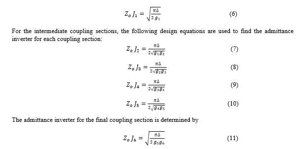
Where is the characteristic impedance with value of 50 Ω , are the values for the elements of the fifth order Chebyshev with 0.5 dB ripple low pass filter prototype, is the admittance inverter constant, and is the fractional bandwidth with value of 0.1. The spacing between the coupled lines, length and width are calculated in ADS using the odd mode (Z0o) and even mode (Z0e) characteristic impedances of the coupled sections. For each coupling section, Z0o and Z0e are calculated by using the following equations:
 Table 1 shows the calculated values of the odd and even impedances for the desired microstrip coupled line BPF [2].
3.6. Design and Simulation of a Low Noise Amplifier
The low noise amplifier (LNA) is used at the input of a receiver to amplify the low level signal with special care to minimize the effect of the unavoidable noise. The appropriate active device ATF-36163 is selected to design the LNA because it has a minimum noise figure and a maximum gain of 0.86 dB and 10.11 dB, respectively, at an operating frequency of 10 GHz. The ADS simulation is carried out to find the stability factor and determine the circles for the constant maximum available gain, and constant noise figure. Then the source reflection coefficient (⎾S) is selected at a point on the Smith chart that achieves an acceptable gain and noise figure according with the design goals. The load reflection coefficient is determined by the following equation.
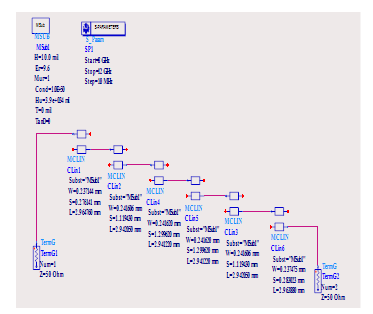 Figure 6: Simulation of a Microstrip Coupled Line Band-Pass Filter using ADS
Table 1: Calculation of Odd and Even Characteristic Impedances
| Coupling section #1 | ||||
| Coupling section #2 | ||||
| Coupling section #3 | ||||
| Coupling section #4 | ||||
| Coupling section #5 | ||||
| Coupling section #6 |
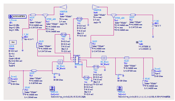 Figure 7: The Complete Circuit Design for the Proposed Low Noise Amplifier
 Figure 8: Simulation of a Microwave Single-Balanced Mixer using ADS
![]() The determined ⎾S and ⎾L are then converted to the source and load impedances, respectively. The input and output matching circuits are designed using microstrip transmission lines [3]. The radial stub is used to prevent the AC signals from entering the DC power supply. The series capacitors are used to block DC signals from entering the source and terminating tuning networks as shown in Figure 7.
The determined ⎾S and ⎾L are then converted to the source and load impedances, respectively. The input and output matching circuits are designed using microstrip transmission lines [3]. The radial stub is used to prevent the AC signals from entering the DC power supply. The series capacitors are used to block DC signals from entering the source and terminating tuning networks as shown in Figure 7.
3.7. Design and Simulation of a Microwave Single-Balanced Mixer
The proposed microwave single-balanced mixer consists of two microwave schottky diodes (HSMS-8101) which are connected via a quadrature hybrid. This mixer provides isolation between local oscillator (LO) and RF inputs. Either the LO or the RF signal is added destructively at the IF port of the mixer. The impedance matching is designed to convert the schottky diode’s impedance into 50 Ω. Figure 8 shows the schematic of the microwave single-balanced mixer [2].
4. Simulation Results
The harmonic balance (HB) simulator in ADS is used to perform the frequency domain analysis for the non-linear circuit of the proposed 10 GHz oscillator. The grounded oscillator port (Oscport) is used to predict the frequency spectrum and the time domain waveform of the oscillation circuit. Figure 9 and 10 show the frequency and time domains of the oscillation where the common gate transistor (ATF-13786) oscillates at 10 GHz.
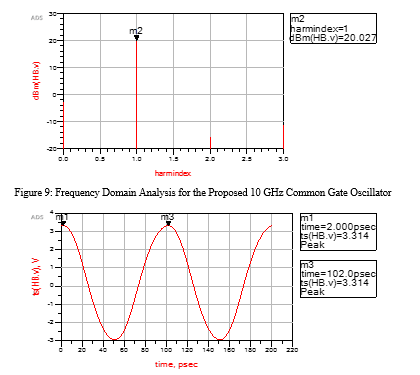 Figure 10: Time Domain Analysis for the Proposed 10 GHz Common Gate Oscillator
The S-parameters versus frequency for the Wilkinson power divider are simulated in ADS as plotted in Figure 11. At frequency of 10 GHz, the reflection coefficient at port 1 is small because the value for S11 is less than ‒40 dB; also the power equal-split between ports 2 and 3 is confirmed because the value of both S21 and S31 is about ‒3 dB.
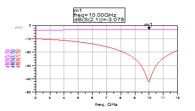 Figure 11: Simulated S-Parameters for Wilkinson Power Divider
The simulated S-parameters in ADS for the class-A power amplifier are shown in Figure 12. The complete circuit for the designed class-A power amplifier is well matched at 10 GHz because S11 is less than ‒30 dB. At a frequency of 10 GHz, the value of S21 indicates that the obtained gain at the output is 8.141 dB.
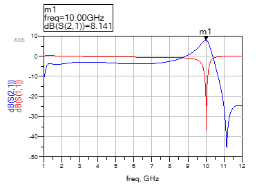 Figure 12: Simulated S-Parameters for the Proposed Class-A Power Amplifier
The CST MWS simulation results for the S-parameters and the three-dimensional radiation pattern for the designed Cantenna are shown in Figures 13 and 14, respectively. This Cantenna can achieve bandwidth of 15 % and gain of 7.755 dB at 10 GHz.
 Figure 13: Simulated S-Parameters for the Proposed Cantenna
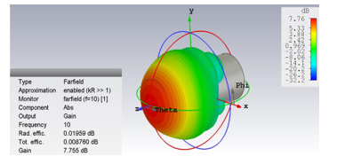 Figure 14: Three-Dimensional Radiation Pattern for the Designed Cantenna
The response of the microstrip coupled line band-pass filter is obtained using ADS simulation as shown in Figure 15. The center frequency is 9.97 GHz, while the band edges frequencies are 9.88 GHz and 10.06 GHz, respectively.
 Figure 15: Simulated Response for the Microstrip Coupled Line Band-Pass Filter
S-parameters of the designed LNA are obtained by using ADS simulation as shown in Figure 16. At 10 GHz, simulations show a gain (S21) of 10.488 dB, the circuit of the designed LNA is well matched because the values of S11 and S22 are ‒14.89 dB and ‒18.29 dB, respectively. Also the designed LNA circuit shows a good isolation because the value of S12 is below ‒16.44 dB.
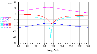 Figure 16: Simulated S-Parameters of the Designed LNA
The designed microwave single-balanced mixer is simulated in ADS. Figure 17 shows the spectrum at the output of the microwave single-balanced mixer; these results are obtained by using the harmonic balance (HB) simulator.
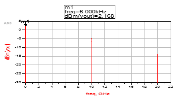 Figure 17: Simulated Spectrum at the Output of the Microwave Single-Balanced Mixer
The individual designed and simulated microwave components are connected together to form the complete RF Front-End transceiver for a continuous wave (CW) Doppler radar. This proposed Doppler radar RF front-end transceiver is simulated in ADS as shown in Figure 18. The amplified 10 GHz continuous wave hits an object. The received reflected wave will have a frequency higher than 10 GHz if the object moves toward the radar. On the other hand, the frequency of the received reflected wave will be lower than 10 GHz when the object moves far from the radar, this phenomenon is known as the Doppler effect. The reflected wave goes to the microstrip coupled line band-pass filter from which it is applied to the LNA, and then the output of the LNA is mixed with a portion of the transmitted wave.
 Figure 18: Complete Schematic of the RF Front-End Transceiver for a Doppler Radar
Figure 19 shows the ADS model of the object, this model simulates how the Doppler frequency is generated by the moving object. The frequency of transmitted continuous wave is shifted by a Doppler frequency ( ). So that the frequency shift in the transmitted continuous wave is simulated by multiplying this transmitted continuous wave with or with . The transmitted continuous wave is equally split by the power divider (PwrSplit2). One of the outputs of (PwrSplit2) goes through a phase-shifter (PhaseShiftSML) with phase shift of or and then it is multiplied by using a multiplier (MULT2), the other output of (PwrSplit2) goes unchanged before it is multiplied by using (MULT1). The outputs of (MULT1) and (MULT2) are combined together using a power combiner (PwrSplit2).
 Figure 19: ADS Model of the Moving Object
The Doppler radar RF Front-End transceiver is simulated using ADS by selecting the Doppler frequency to be 6000 Hz as shown in Figure 19. The output of the microwave single-balanced mixer is filtered out using a low pass filter (LPF). At the output of the LPF, the frequency of the received continuous wave is confirmed to be equal the generated Doppler frequency as indicated in Figure 20.
 Figure 20: Time Domain of the Received Signal at the Output of the Low Pass Filter
5. Conclusions
Each microwave component of the continuous-wave radar RF front-end transceiver has been designed and simulated individually including 10 GHz oscillator, Wilkinson power divider, class-A power amplifier, Cantenna, microstrip coupled line band pass filter, low noise amplifier and microwave single balanced mixer. The microwave components have been connected together to form the complete schematic of RF front-end transceiver for a CW Doppler radar, then the proposed system has been simulated using ADS. This strategy in teaching the microwave engineering course uses the electromagnetics simulation tools such as ADS and CST and the theoretical knowledge in order to practice designing the microwave components.
Conflict of Interest
The author declares no conflict of interest regarding the publication of this paper.
- E. Aydin and N. E. Çagiltay, “Use of advanced technologies in a RF and Microwave Engineering course,” IEEE EDUCON 2010 Conference, Madrid, pp. 811-817, 2010. doi: 10.1109/EDUCON.2010.5492495
- D. M. Pozar, Microwave engineering. Hoboken, NJ: Wiley, 2012.
- K.-W. Yeom, Microwave circuit design: a practical approach using ADS. New York: Prentice Hall, 2015.
- Teng, Kevin Chi-Ming, “The Design and Evaluation of a 5.8 GHz Laptop-Based Radar System” Master Thesis, Purdue University, 2013.