
Material, Structural Optimization and Analysis of Visible-Range Back-Illuminated OPFET photodetector
Volume 4, Issue 4, Page No 485-502, 2019
Author’s Name: Jaya V. Gaitondea), Rajesh B. Lohani
View Affiliations
Electronics and Telecommunication Department, Goa Engineering College, Farmagudi-Ponda-Goa, 403401, India
a)Author to whom correspondence should be addressed. E-mail: jayagaitonde46@gmail.com
Adv. Sci. Technol. Eng. Syst. J. 4(4), 485-502 (2019); ![]() DOI: 10.25046/aj040459
DOI: 10.25046/aj040459
Keywords: Material optimization, Structural optimization, Back-illuminated OPFET, Photodetector, Visible range, Visible/UV contrast ratio

Export Citations
High gain-bandwidth product and visible/UV contrast photodetectors are vital in Visible Light Communication (VLC) and Ultraviolet (UV) reflectance imaging applications respectively. We adopt material and structural optimization to perceive such photodetectors with back-illuminated Optical Field Effect Transistor (OPFET) wherein any potential difference in absorption coefficient of the semiconductor material between the visible and the UV range (higher in the UV region) can be explored at its full potential. The results have been analyzed using the photoconductive and the photovoltaic effects, the series resistance effects, scaling rules- induced effects, and channel length-variation effects. We consider the three most prominent and functional materials in the visible range (Si, GaAs, and InP) for material-based optimization. Structural optimization is performed employing a range of medium gate lengths. The gate electrodes utilized are Indium-Tin-Oxide (ITO) for Si and GaAs with high Schottky barrier heights of ~0.71 eV and ~0.98 eV respectively whereas the Schottky contact on InP is gold (Au) with a high barrier height of ~0.8 eV. The operating visible and UV wavelengths are 600 nm and 350 nm respectively. The results suggest that GaAs OPFET has wide bandwidth potential in the gigahertz range apart from its high sensitivity and visible/UV contrast features. The InP-based OPFET exhibits high sensitivity and sub-gigahertz frequency response; and can compete or surpass the GaAs OPFET in terms of the visible/UV contrast ratio. The Si OPFET shows bandwidth in the megahertz range along with high sensitivity but exhibits low contrast ratio. The structural parameters have a significant effect on the detector response. The results are in-line with the experiments. This paper reflects the performance of the investigated detectors towards the said applications through optimization and the associated analysis represents the dependence of the obtained response on the device material and structural parameters, thus, opening the door for further research.
Received: 16 June 2019, Accepted: 02 August 2019, Published Online: 21 August 2019
1. Introduction
This paper is an extension of work originally presented in The IEEE Conference on Emerging Devices and Smart Systems (ICEDSS’18) [1].
Visible-Light Communication (VLC) is an emerging alternative to RF-based communication to suffice for the increasing demand for bandwidth. Its potential applications include Li-Fi (Light-Fidelity) Networks, vehicle to vehicle communication, robots in hospitals, underwater communication, and information displayed on sign boards [2]. The photodetectors contributing to VLC should feature high gain-bandwidth product apart from low dark current. Presently, the state-of-art photodetectors being employed in VLC include the p-i-n and the Avalanche photodiodes (APDs). p-i-n detectors provide high speed detection but without amplification whereas the APDs offer high gain but as the frequency increases, the gain reduces significantly. On the other hand, Ultraviolet (UV) reflectance imaging is a well-known application in biomedical engineering. It requires photodetectors with high visible/UV contrast ratios alongwith high visible sensitivity and low dark current. There is no much information available on the visible/UV contrast features of any photodetector. The contrast ratio should be high in order to appropriately control the ambient visible light in the presence of background UV radiation during imaging and enabling erroneous operation. Low dark current improves the device performance. Both the applications have one thing in common: they need photodetectors operating in the visible range. Three most featured materials capable of operating in the visible region include Si, GaAs, and InP. These possess distinct electrical and optical properties which motivate one to conduct research using these materials. One potential candidate to cater to high gain-bandwidth product applications is a phototransistor or a photoFET. Optical Field Effect Transistor (OPFET) or optically controlled Metal-Semiconductor Field Effect Transistor (MESFET) has been a widely studied device over the past few decades for its applications as photodetectors, optically-controlled amplifiers, oscillators, and switches [3]-[13]. However, the research lacks the assessment or the impact of the OPFET device incorporating these materials from the optimization point of views i.e. material and structural optimization. Further, analysis of the attained results and the correlation of the detector responses with the material and the structural parameters can substantiate further research. Thus, in this paper, we call for material and structural optimization of the visible-range back-illuminated OPFET detector for communication and visible/UV contrast applications. The back-illuminated OPFET model (without substrate effect) is purposely chosen so that any significantly high difference in absorption coefficient at the visible and UV wavelengths is potentially used for contrast applications. The transparent gate materials considered for simulation are Indium-Tin-Oxide (ITO) for Si and GaAs whereas gold (Au) for InP. The corresponding barrier heights are ~0.71 eV, ~0.98 eV, and ~0.8 eV respectively. Possibly large barrier heights have been chosen since these can have considerable positive effect on the photovoltage and the photoconductive effect through the modulation of the depletion width.
A theoretical semi-analytical model accounting for photoconductive and photovoltaic effect is presented. The continuity equations have been solved analytically to yield the carrier densities whereas the charges are calculated numerically using the Trapezoidal method. The total drain-to-source current is estimated using the model given in [14]. The trap effects have been neglected in this work.
We begin with the theory followed by the results, discussion, and the relevant analysis. We conclude with a brief summary.
2. Theory
The back-illuminated device structure is schematically shown in Fig. 1. The gate is shorted to the source for a reduction in the number of power supplies. The channel is n-type uniformly moderately doped whereas the substrate is p-type semi-insulating. The illumination is guided by a fiber inserted from the rear side of the device through the substrate upto the active layer-substrate interface. The radiation is absorbed in the channel and the substrate regions creating electron-hole pairs. The holes contribute to photovoltage after crossing the Schottky junction which increases the drain-to-source current through a reduction in the depletion width (photovoltaic effect). On the other hand, the electrons are directed toward the channel which increases its conductivity upon the application of the drain-to-source voltage (photoconductive effect).
The device characteristics are depicted by the three regions of operation: the linear, the pinch-off, and the saturation regions. The drain-to-source saturation current depends upon the total charge, the gate width, and the saturation velocity and is limited by the voltage drop across the source series resistance. The drain-to-source conductance also depends upon the total charge (however, at zero drain-to-source voltage), the carrier mobility, and the gate width; is inversely proportional to the gate length, and is limited by the source and drain series resistances. The total drain-to-source current is given by [14]:
![]() where the symbols have the same meaning as stated in [14]. The parameter η is defined as the ratio of the drain-to-source conductance to the saturation current as the drain-to-source voltage tends to zero. Thus, on one hand, the drain-to-source current is directly proportional to the saturation current; on the other hand it is inversely proportional to the saturation current through the parameter η under the hyperbolic tangent expression. This shows that there is limitation on the total current that can be achieved. The parameter η also signifies that the total current is directly proportional to the conductance as VDS tends to zero under the hyperbolic tangent expression. Hence, the conductance as VDS tends to zero and the saturation current are the prominent factors determining the total drain-to-source current apart from the voltage, VDS, and the total current is limited by the source and drain series resistances.
where the symbols have the same meaning as stated in [14]. The parameter η is defined as the ratio of the drain-to-source conductance to the saturation current as the drain-to-source voltage tends to zero. Thus, on one hand, the drain-to-source current is directly proportional to the saturation current; on the other hand it is inversely proportional to the saturation current through the parameter η under the hyperbolic tangent expression. This shows that there is limitation on the total current that can be achieved. The parameter η also signifies that the total current is directly proportional to the conductance as VDS tends to zero under the hyperbolic tangent expression. Hence, the conductance as VDS tends to zero and the saturation current are the prominent factors determining the total drain-to-source current apart from the voltage, VDS, and the total current is limited by the source and drain series resistances.
Under illumination, the total charge is boosted due to the photovoltaic and the photoconductive effects which enhances the saturation current and the drain-to-source conductance limited by the series resistances. In addition, with the increase in the optical power, the photovoltage increases reducing the series resistances and augmenting the current. The source and drain series resistances are calculated based on the method provided in [15]. The reader is advised to follow [1] for the modeling equations and the calculation of the carrier densities, photovoltage, and the total charge.
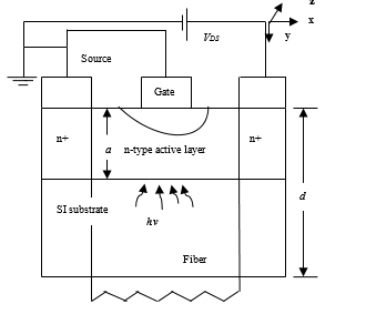 Figure 1. The schematic structure of the back-illuminated model of OPFET.
The detector parameters such as responsivity, dark current, and visible/UV contrast ratio are defined in [1]. Here we define the 3-dB bandwidth and the unity-gain cut-off frequency (fT) of the device. The bandwidth is the highest modulation frequency which the photodetector can detect without errors. Mathematically, it is given by the frequency at which the photocurrent response falls to 0.707 times its DC response. The unity-gain cut-off frequency is the operating frequency at which overall gain of the device falls to unity. The fT is given by the ratio of the transconductance to 2π times the gate-to-source capacitance. The transconductance is the variation in the drain-to-source current with the variation in the gate-to-source voltage and is the amplification factor. The gate-to-source capacitance is the change in the space charge below the gate and its sidewalls with the change in the gate-to-source voltage and is a switching parameter. Thus, fT represents the amplification bandwidth of the device. The simultaneous detection-cum-amplification bandwidth is given by either of the two (3-dB bandwidth or the fT value), whichever is smaller.
3. Results and Discussion
The simulations have been carried out in MATLAB with MEX coding feature. The results have been validated with experimental work published elsewhere [3] (Figure 2). The results have been compared with the commercially available software (Visual TCAD)-based simulations and have shown close resemblance (Figure 3) (Gate length of 4 μm, gate width of 4 μm, active layer thickness of 0.27 μm, and doping concentration of 4×10²² /m3). The drain-to-source bias voltage is variable whereas the gate-to-source voltage is set to zero volts. The wavelengths used are 600 nm for the visible light and 350 nm for the UV radiation. The photon flux densities of 1016, 1019, and 1022 /m2-s used in these simulations correspond to optical power densities of 0.33 μW/cm2, 0.33 mW/cm2, and 0.33 W/cm2, respectively at 600 nm and 0.57 μW/cm2, 0.57 mW/cm2, and 0.57 W/cm2 respectively at 350 nm. The structural optimization is performed over a wide range of medium gate lengths from 3 μm to 5 μm. However, only the four most relevant sets are provided here for comparison. The design variables are chosen based on the scaling rules stated in [16]. The materials being employed are Si, GaAs, and InP for the back-illuminated OPFET device with the gate electrodes being Indium-Tin-Oxide (ITO) for Si and GaAs, and gold (Au) for InP. The simulated optimization results are presented in Table I. The parameters used for calculation are given in Table II. The comparison with the state-of-art photodetectors and amplifiers is provided in Table III showing significantly enhanced response. Figure 4 depicts the drain-to-source current responses under dark and illumination for all the three devices at a gate length of 3 μm and an active layer thickness of 0.27 μm at an intensity of 1019 /m2-s clearly showing the sensitivity to visible light. Figure 5 portrays the frequency responses of the three devices at a gate length of 3 μm and an active layer thickness of 0.27 μm at an intensity of 1019 /m2-s demarcating that the GaAs, InP, and Si OPFET devices operate at high, moderate and low data frequency ranges respectively.
3.1. Series resistance and photovoltage analysis in Si, InP, and GaAs OPFETs
Beginning the discussion with the Si back-illuminated OPFET, this device exhibits the largest series resistances among all the material devices with similar dimensions in the visible range. With the smallest Schottky barrier height of ITO-Si junction (~0.71 eV), the series resistance ought to be the smallest due to the larger undepleted channel thickness in the spacing between the gate and the source, and the gate and the drain (depletion width is dependent upon the barrier height). This should have drawn larger current through the channel charge. However, due to the low electron mobility (~0.09 cm2/(V.s)) and the said barrier height, upon which the current flowing in the spacing between the gate and the source, and the gate and the drain depends upon (barrier height directly affects the voltage drop across the channel), the current significantly falls. This raises the series resistance value to compensate for the fall with the increment in the depletion width through the voltage drop across the series resistance. Other materials, GaAs and InP exhibit lower and almost equal series resistances. This is attributed to the higher mobility of GaAs (~0.5 cm2/(V.s)) and higher barrier height of ITO-GaAs junction (~0.98 eV) (through the voltage drop) which tend to increase the current in the spacing and lower the resistance. The same barrier height also tends to decrease the current (through the increment in the depletion width) and raise the resistance, however, the factors supporting the lowering of the resistance supersede those raising it, resulting in net reduction of resistance. For InP, the mobility is (~0.43 cm2/(V.s)) and the barrier height of Au-InP junction is (~0.8 eV). In this case, the mobility is significantly high whereas the barrier height is moderate. With the moderate barrier height, the series resistance ought to be between that of Si and GaAs, but due to the high mobility the series resistance in InP features the same as that in GaAs. The series resistances play an important role in limiting the photocurrent. The series resistances decrease with illumination.
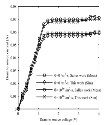 Figure 2 Comparison of the present model results with the experiments in [3].
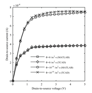 Figure 3 Comparison of the present model results with the simulations using Visual TCAD Software.
The photovoltage generated is almost the same in both Si and InP devices (~0.27 V, ~0.46 V, and 0.61 V) in the visible range considering most of the sets. This can be explained as follows: The photovoltage depends upon the photogenerated hole density crossing the Schottky junction which in turn, depends upon the absorption coefficient, the photon flux density, the hole lifetime, and the saturated hole velocity. The absorption coefficient of Si at 600 nm is 7.5×10⁵ /m, the hole lifetime is 75 μs, and the saturated hole velocity is (~6.3×10⁴ m/s). On the other hand, the corresponding parameters for InP are 1×10⁷ /m, 0.3 μs, and (~5.6×10⁴ m/s) respectively. The hole density is directly proportional to the absorption coefficient, the photon flux density, and the hole lifetime (αΦτp), whereas it is inversely related to the saturated hole velocity through (1+αvyτp).The values suggest that the terms directly as well as inversely related to the hole density are almost the same in both the cases since any difference in individual parameters between the two material systems is cancelled out when their product is evaluated. One more parameter upon which the photovoltage is dependent upon is the reverse saturation current density through the Schottky barrier height. The photovoltage is inversely related to the saturation current density, and the saturation current density is inversely related to barrier height. Hence, the photovoltage is directly related to barrier height. Since, the barrier heights of ITO-Si andAu-InP junctions are (~0.71 eV) and (~0.8 eV) respectively, the photovoltage tends to be more in the InP device. However, since InP possesses a high absorption coefficient of 1×10⁷ /m corresponding to an absorption depth of 0.1 μm, the hole density experiences an exponential decrease with distance and fewer holes cross the Schottky junction as compared to the Si device. The moderate absorption coefficient of 7.5×10⁵ /m results in a large absorption depth thus, causing a lesser degradation of hole density with distance. As a result, the photovoltage developed is almost the same in both the cases. On the other hand, the photovoltage generated in GaAs OPFET is enhanced (~0.398 V, ~0.576 V, and ~0.755 V). This is due to the moderate absorption coefficient of GaAs in the visible region (4×10⁶ /m), the higher saturated hole velocity (~9×10⁴ m/s), and the significantly higher Schottky barrier height of the ITO-GaAs junction (~0.98 eV) superseding the effect of lower hole lifetime (10-8 s). The saturated hole velocity positively affects the photovoltage through the photogenerated hole current density in the equation for photo voltage.
At the lowest gate length under consideration of 3 μm and the highest doping concentration of 5×10²² /m3 (gate length-doping concentration product is constant from scaling rules [16]) with an active layer thickness of 0.15 μm, the OPFET devices exhibit the lowest dark and photocurrents among all the sets. This is ascribed to the very less active-layer thickness, as well as the low gate length and the gate width along with the reduced sensitivity at the higher doping concentrations. This proportionally decreases the current although the high doping concentration induces significant channel charge.
3.2. Analysis of Si OPFET at 3 µm gate length and 0.15 µm channel thickness
The drain-to-source currents obtained using Si OPFET are (0.36 mA, 0.9 mA, 1.7 mA, and 15.6 mA). The large series resistances owing to the small active layer thickness (0.15 μm) and significantly high barrier height (~0.71 eV) limit the said currents. At the flux density of 1016 /m2-s, the photovoltaic effect is significant (0.28 V) whereas the photoconductive effect is negligible as compared to the photovoltaic effect (due to the lower power level) resulting in a current of 0.9 mA. The photoconductive effect will add to the response only when the photoconductive charge is comparable to the doping-induced charge. As the flux density is increased to 1019 /m2-s, the photoconductive effect also contributes in addition to the photovoltaic effect (0.46 V) owing to the higher power level and the long electron lifetime (75 μs). Most of the photoconductive contribution emanates from the depletion region since the major portion of the channel is depleted owing to high barrier height, small channel thickness, and the large series resistance which incurs significant voltage drop across it. This results in a quite high current of 1.7 mA. At the flux density of 1022 /m2-s, the current is significantly enhanced (15.6 mA) owing to the considerably high contribution from the photoconductive effect in the depletion region. There is no photovoltaic contribution; instead the device shows negative sensitivity i.e. increase in depletion width with illumination. This arises due to the substantially high current from the photoconductivity which incurs large voltage drop across the series resistance. Thus, the depletion width increments with illumination surpassing the effect of photovoltage-induced reduction of the depletion width. As such, the responsivities attained are (5.3×10⁸ A/W, 1.32×10⁶ A/W, and 1.49×10⁴ A/W) which are significantly high owing to the above discussed phenomena and the low dark current. The 3-dB bandwidths exhibited by this device are (0.16 MHz, 0.136 MHz, and 0.57 MHz). These megahertz range bandwidths are due to the long electron and the hole lifetimes (75 μs) upon which the bandwidth is inversely related through the modulation of carrier lifetime with frequency. At the lowest flux density, the bandwidth is 0.16 MHz due to the contribution from the photovoltaic effect alone. At the higher flux density, the bandwidth falls to 0.136 MHz due to both photovoltaic and photoconductive effects adding to the response.
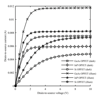 Figure 4 Comparison of the Si, InP, GaAs OPFET devices under dark and illumination.
This can be explained by the fact that when the identical frequency responses of two independent comparable effects are added, the net frequency response exhibits reduced bandwidth as compared to the individual ones. As the flux density is increased further, the bandwidth rises to 0.57 MHz. This is attributed to the sole and substantially high contribution from the photoconductive charge as compared to the previous responses. The transconductances obtained are the lowest among all the sets (1.4 mS, 2.4 mS, 3.9 mS, and 29.1 mS) due to the reduced dimensions at this gate length which decreases the overall current and the reduced sensitivity at high doping concentrations. Note that at constant photovoltage, the depletion width sensitivity is higher at lower doping concentrations. The transconductance increases with the increase in the optical power [6], [7], [9], [10] since at a constant doping concentration, the depletion width sensitivity is higher at larger photovoltages. However, at the highest flux density, this does not hold good where the device experiences negative sensitivity. In this case, it is the high photoconductive charge which results in high saturation current and is independent with the change in the gate-to-source voltage due to the complete depletion of the channel. The drain-to-source conductance evaluated at zero drain-to-source voltage also is high due to the induced charge and is sensitive to the variation in the gate-to-source voltage since the channel is undepleted (zero drain-to-source voltage). Further, the conductance is affected by the dependence of the series resistances on the gate-to-source voltage. The above reasons suffice for the observed high transconductance. The gate-to-source capacitances are also the lowest among all the sets (0.0546 pF, 0.084 pF, 0.105 pF, and 0.0076 pF) owing to the same reasons as applicable to the transconductances, however, here the gate region space charge replaces the drain-to-source current. The reasons hold good for the lower flux densities. However, at the higher flux density, the space charge is considerably reduced due to the photoconductive electrons in the depletion region de-ionizing the charged donor ions. Also, the gate-to-source capacitance is independent of the change in the photoconductive charge (which is a major contributor to the response) since it is a measure of the space charge variation with the gate-to-source voltage. These reasons explain the significant drop in the capacitance at the higher flux density. As such, the unity-gain cut-off frequency attained is (4.08 GHz, 4.53 GHz, 5.89 GHz, and 606.7 GHz). Under UV illumination of 350 nm, the photovoltage is slightly enhanced (0.31 V, 0.49 V, and 0.61 V) as compared to that under visible light since Si possesses a larger absorption coefficient of 1×10⁷ /m at the UV wavelength. The smaller active layer thickness (0.15 μm) enables significant number of holes to cross the junction before the generated carriers experience degradation due to the dependence on the distance. The series resistances experienced by the device are almost the same due to the slight difference between the photovoltages. The drain-to-source current is almost the same at the lower intensity (1 mA) whereas there is a considerable boosting of the current at the higher intensities. This is attributed to the large absorption coefficient of Si under UV light which augments the photoconductive charge in the depletion region. At these intensities, the large currents develop large voltage drops across the series resistances thus inducing negative sensitivity and eliminating the photovoltaic contribution. The currents so obtained are 7.9 mA and 16.1 mA. The lesser enhancement of current at the flux density of 1022 /m2-s is due to the limitation of the drain-to-source conductance (at zero drain-to-source voltage) by the series resistances and the large saturation current due to the induced charge also limiting the factor η as discussed earlier thus, restricting the total drain-to-source current. As such, the responsivities attained are (3.53×10⁸ A/W, 4.33×10⁶ A/W, and 9×10³ A/W). The responsivities at the flux densities of 1016 and 1019 /m2-s are slightly lower than the visible range responsivities. This is because the device uses more power to detect UV light than the visible light since the power is directly proportional to the photon energy. Hence the visible/UV rejection or the contrast ratios are very low (1.5, 0.3, and 1.65).
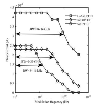 Figure 5 Frequency responses of the Si, InP, GaAs OPFET devices.
3.3 Analysis of InP OPFET at 3 µm gate length and 0.15 µm channel thickness
Discussing the InP OPFET with a gate length of 3 μm and an active layer thickness of 0.15 μm, the photovoltage is slightly enhanced (0.297 V, 0.476 V, and 0.65 V) as compared to the Si OPFET due to the small active layer thickness which eliminates the degradation of the generated carriers with distance as would occur in other cases. The series resistances are significantly lower than the Si OPFET but comparatively higher than that at higher gate length devices due to the reasons discussed earlier. The conducting photovoltaic charge is higher in the case of the InP OPFET in the presence of series resistances. This is because, the Si device possesses larger series resistances which incurs considerable voltage drop across these resistances thus, limiting the photovoltaic effect. Further, the photovoltage is slightly higher in the InP detector. This charge determines the saturation current. Hence, the saturation current is higher in the InP device. The conducting photovoltaic charge in the absence of series resistances i.e. at VDS=0 V, is lower in the case of InP OPFET. The above emanates from the fact that at a fixed doping concentration and at a given gate-to-source voltage, the depletion width sensitivity to illumination is higher in both the lower barrier height and the lower dielectric constant device i.e. Si device. This charge determines the drain-to-source conductance at VDS=0 which is higher in the Si OPFET however, is limited by the presence of series resistances which are larger in the case of Si detector. One more factor which differentiates the two devices is the electron mobility upon which the conductance depends upon and is substantially higher in the case of InP. The dark current is lower in the InP device due to the higher barrier height. The above factors result into slightly higher photovoltage-induced currents (1.3 mA, and 2.2 mA) in the InP OPFET than the Si OPFET. At the flux density of 1022 /m2-s, the photoconductive charge from the depletion region alone contributes since the device exhibits negative sensitivity as mentioned earlier and the channel is totally depleted. The InP detector generates a current of 27.8 mA as opposed to 15.6 mA in the Si OPFET. This can be explained as follows: Since the absorption coefficient of Si is moderate (7.5×10⁵ /m), there is almost uniform photogeneration throughout the fully depleted channel of 0.15 μm thickness. The absorption coefficient of InP is high (1×10⁷ /m) due to which only a part of the depletion region carries significant number of carriers. Thus, the contributing charge is one order higher in the case of Si OPFET than the InP OPFET. This results in a large saturation current in the Si device. However, the conductance is lower in the Si device owing to lower electron mobility and larger series resistances. Since the saturation current appears in the numerator and as well as the denominator (through the hyperbolic tangent expression (see (1))), the large saturation current also limits the total drain-to-source current in the Si device. As a cumulative effect, the current is larger in the InP OPFET. These currents are the lowest among all the sets due to the reasons discussed earlier in the case of the Si OPFET. The 3-dB bandwidths achieved are (67.35 MHz, 0.26 GHz, and 3.84 MHz). These bandwidths are higher than that in Si OPFET owing to the shorter hole and electron lifetimes (0.3 μs) in InP as compared to 75 μs in Si. The boosting of the photovoltage as the intensity is increased from 1016 to 1019 /m2-s also boosts the bandwidth from 67.35 MHz to 0.26 GHz. At the flux density is raised to 1022 /m2-s, the bandwidth drops to 3.84 MHz due to the following: Under dc conditions or at lower frequencies, the photoconductive effect is significantly high and is the sole contributor. However, as the frequency is increased, the photoconductive contribution starts decreasing due to the dependence of the electron lifetime on frequency. This reduces the voltage drop across the series resistance thus, widening the effective channel width and increasing the photovoltaic contribution. Hence, at the juncture of the 3-dB point, both the effects effectively contribute causing the drop in the bandwidth. The responsivities attained are (9.97×10⁸ A/W, 1.9×10⁶ A/W, and 2.7×10⁴ A/W) which are higher than that in the Si device due to larger photocurrents. The InP detector exhibits transconductances of (2.3 mS, 4.3 mS, 5.6 mS, and 6.7 mS). These values are higher than that for Si OPFET except at the flux density of 1022 /m2-s. As explained earlier, the saturation currents, the drain-to-source conductances, and the mobility involved are higher in the InP device whereas the series resistances are lower in the InP device at the lower intensities. The depletion width sensitivity to the applied gate-to-source voltage with the other factors kept constant is higher in the lower barrier height and the lower dielectric constant device (Si OPFET). But, in practice, due to larger series resistances and the lower mobility of Si, the net effect is the larger sensitivity in the InP device. Further, the photovoltage is slightly larger in the InP device. Due to the above factors, the transconductances are higher in the InP OPFET at the lower flux densities. But at the intensity of 1022 /m2-s, the channel is fully depleted. The depletion state does not affect the saturation current in terms of magnitude (it grows without bounds in spite of the presence of the series resistances). This is because, when the channel gets depleted (due to the large voltage drop across the series resistances), it is the photoconductivity in the depletion region which takes over role of the otherwise contributing photoconducting charge from the neutral channel region. Since the photoconductive charge in Si OPFET is very high and one order higher than that of the InP OPFET, the saturation current is considerably higher in the Si device. This current is insensitive to the applied gate-to-source voltage owing to the complete depletion of the channel. However, the drain-to-source conductance changes with the gate-to-source voltage since it is evaluated at VDS=0 which means a finite undepleted channel width. This conductance is lower in magnitude as well as less sensitive to the change in the gate-to-source voltage in the Si detector due to the lower mobility and limiting effects of the series resistances. But, the effect of very large saturation current in the Si device supersedes the effect of lower conductance and its sensitivity to generate higher transconductance. The transconductance increases with the increase in the optical intensity due to the enhancement of the photovoltaic effect upto the flux density of 1019 /m2-s and high contribution of photoconductive effect at the intensity of 1022 /m2-s. On the whole, the transconductances obtained at this gate length are the lowest among all the sets due to the reasons stated earlier for the Si OPFET. The gate-to-source capacitances attained in the InP device are (0.034 pF, 0.0695 pF, 0.092 pF, and 0.016 pF). These values are lower than that of Si device. This is explained by the fact that at a constant or slightly varying photovoltage and a fixed doping concentration, the depletion width sensitivity to the applied gate-to-source voltage is larger for the lower barrier height (and dielectric constant) device i.e. Si OPFET. The capacitances increase with optical power and fall at the highest flux density and are lowest among all the sets due to the same reasons as described earlier in the case of Si device. The unity-gain cut-off frequencies thus obtained are (10.76 GHz, 9.74 GHz, 9.65 GHz, and 65.4 GHz). Under UV illumination, the photovoltages developed are substantially lower (0.0943 V, 0.27 V, and 0.44 V) than that in the visible region owing to the very high absorption coefficient of InP in the UV region (7.6×10⁷ /m).This generates significantly large number of carriers only upto a small distance from the absorption surface (i.e. the active layer-substrate interface). The generated carriers crossing the Schottky junction are considerably low due to the significant degradation of the carriers with distance (the active-layer thickness (0.15 μm) is much larger than the absorption depth (0.013 μm)). The drain-to-source currents obtained are (0.272 mA, 0.54 mA, 1.2 mA, and 30.1 mA). Due to the lesser photovoltages, the currents obtained are lower in the UV region upto the intensity of 1019 /m2-s. At the flux density of 1022 /m2-s, the current is higher (30.1 mA) owing to the substantially high contribution from the photoconductive effect in the depletion region emanating from the larger absorption coefficient of InP in the UV region. The photovoltaic effect plays no role at this intensity since the device exhibits negative sensitivity. The responsivities obtained are (1.53×10⁸ A/W, 5.2×10⁵ A/W, and 1.71×10⁴ A/W) based on the above photocurrents and further assisted by the fact that the device uses more optical power in the UV region than the visible region. The visible/UV contrast ratios obtained are (6.516, 3.65, and 1.58).
3.4. Analysis of GaAs OPFET at 3 µm gate length and 0.15 µm channel thickness
Discussing the GaAs OPFET device possessing a gate length of 3 μm and an active-layer thickness of 0.15 μm, this device develops photovoltages of (0.41 V, 0.58 V, and 0.76 V) in accordance with [7] which are substantially higher than the Si and the InP devices. Under dark, the channel is totally depleted on account of a large Schottky barrier height of ITO-GaAs junction (0.98 eV). Thus, the current from the device channel ceases to exist but there is a small current flowing in the device due to the presence of the shunt resistance. The higher photovoltages ought to have produced larger photovoltaic charge responses as compared to the other detectors (InP OPFET). However, since the channel is deeply depleted (beyond the active-layer thickness), the developed photovoltages do not open the channel wide enough (of course, limited by the series resistances) as opposed to the InP device. The InP device is partially depleted under dark and the generated photovoltages (0.297 V, 0.476 V, and 0.65 V) are able to significantly reduce the depletion width thus yielding greater photovoltaic charges than the GaAs device. In spite of this, the drain-to-source currents (97.1 μA, 1.4 mA, 2.5 mA, and 54.9 mA) and the transconductances (0, 5.5 mS, 7.5 mS, and 67.2 mS) achieved in GaAs OPFET under illumination are higher than the InP device. This is attributed to the higher electron saturated velocity (1.2×10⁵ m/s) of GaAs as compared to InP (7.6×10⁴ m/s) which considerably increases the saturation current further assisted by slightly lower source series resistance in GaAs. Also, the slightly higher electron mobility of GaAs (0.5 m2/(V.s)) as compared to InP (0.43m2/(V.s)) and the lower source and drain series resistances in the GaAs device enhances its drain-to-source conductance even if the conductance in the absence of series resistances is almost the same in both the devices. As a result, the higher currents are attained. The larger transconductances emanate from the amplification of the charge due to the depletion width sensitivity to the applied gate-to-source voltage by the higher electron saturation velocity in GaAs producing larger change in the saturation current. Further, the amplification of the said charge under the absence of series resistance by the higher mobility of GaAs so also the lower series resistances results in larger variation in the drain-to-source conductance. This, on the whole, produces a larger change in the drain-to-source current with the applied gate-to-source voltage. Also, the photocurrents are slightly enhanced due to the lower dark current. At the flux density of 1022 /m2-s, the photocurrent as well as the transconductance are considerably enhanced. This is owing to the boosting of the saturation current and the conductance due to the substantially high contribution from the photoconductive effect in the depletion region as a result of moderate absorption coefficient of GaAs and one order of magnitude higher lifetime (1 μs). The transconductance is much higher than the other two devices because of high saturation current and greater magnitude of the drain-to-source conductance as well as its higher sensitivity to the applied gate-to-source voltage. The gate-to-source capacitances under illumination (0.064 pF, 0.086 pF, and 0.018 pF), on the whole, are lower than the other devices due to the earlier stated fact that the sensitivity of depletion width to the change in the gate-to-source voltage is higher with devices bearing lower barrier height and lower dielectric constant when other factors are almost constant. The capacitance dependence upon the optical power is the same as analyzed with other devices. As such, the fT values attained are (13.68 GHz, 13.79 GHz, and 596.5 GHz). The 3-dB bandwidths exhibited by the device are (1.5 GHz, 6.3 GHz, and 1.1 MHz) which are considerably higher than the other two detectors at the lower intensities owing to the significant photovoltaic effect and lower hole lifetime (10-8 s) with the photovoltage increasing with the optical power. However, at the higher intensity, the bandwidth falls due to the significant sole contribution from the photoconductive effect with a large electron lifetime of 1μs. The responsivities obtained are (1.24×10⁹ A/W, 2.4×10⁶ A/W, and 5.37×10⁴ A/W) in line with [27] which are larger than the other two devices due to larger photocurrents. Under UV light, the response falls significantly (1.57×10⁸ A/W, 6.4×10⁵ A/W, and 2.56×10⁴ A/W), due to the lower photovoltages (0.19 V, 0.37 V, and 0.55 V) owing to the larger absorption coefficient of GaAs (8×10⁷ /m) which enables lesser hole density to traverse the Schottky junction. In this case, the significantly high generation takes place only at or near the absorption surface. Also, the larger photoconductive charge contribution at the high intensity of 1022 /m2-s, emanating from more than one order of magnitude larger absorption coefficient of GaAs than that in the visible region produces large saturation current and large conductance wherein the large saturation current limits the total current. The currents obtained are as (97.1 μA, 0.37 mA, 1.2 mA, and 44.9 mA). The contrast ratios obtained are (7.9, 3.75, and 2.1).
3.5. Comparative Analysis of Si, InP, and GaAs OPFETs at 3 µm gate length and 0.27 µm channel thickness
As the active layer thickness is widened to 0.27 μm, keeping the gate length constant at 3 μm, the series resistances are significantly reduced owing to the wider thickness. However, they are still higher in the Si device as compared to the other two devices. The photovoltage remains almost the same in the Si and the GaAs OPFETs whereas it is slightly decreased in the InP OPFET explained by the possession of moderate absorption
Table 1: Comparative Studies of Si, InP, and GaAs OPFET detectors (1st set)
|
Si back-illuminated OPFET with ITO gate (vgs=0 V, Vds=10 V, λ=600 nm (visible) and 350 nm (UV) 1st set (L=3 μm, Z=100 μm, tsm=0.15 μm, Ndr=5×10²²/m3) |
|||||||||||
| Visible | UV | ||||||||||
| Photon Flux Density (/m2-s) | Photo-voltage (V) | Drain-to-source current (A) | Responsi-vity (A/W) |
Trans-con-ductance (S) |
Gate-to-source capacitance (F) |
fT(Hz) | Band-width (Hz) | Photo-voltage (V) | Drain-to-source current (A) | Responsivity (A/W) | |
| 0 | 0 | 0.36 mA | —— | 1.4 mS | 0.0546 pF | 4.08 GHz | ——- | 0 | 0.36 mA | —— | |
| 1016 | 0.28 V | 0.9 mA | 5.3×10⁸ | 2.4 mS | 0.084 pF | 4.53 GHz | 0.16 MHz | 0.31 V | 1 mA | 3.53×10⁸ | |
| 1019 | 0.46 V | 1.7 mA | 1.32×10⁶ | 3.9 mS | 0.105 pF | 5.89 GHz | 0.136 MHz | 0.49 V | 7.9 mA | 4.33×10⁶ | |
| 1022 | 0.606 V | 15.6 mA | 1.49×10⁴ | 29.1 mS | 0.0076 pF | 606.7 GHz | 0.57 MHz | 0.61 V | 16.1 mA | 9×10³ | |
|
InP back-illuminated OPFET with Au gate (vgs=0 V, Vds=10 V, λ=600 nm (visible) and 350 nm (UV) 1st set (L=3 μm, Z=100 μm, tsm=0.15 μm, Ndr=5×10²²/m3) |
|||||||||||
| Visible | UV | ||||||||||
| Photon Flux Density (/m2-s) | Photo-voltage (V) | Drain-to-source current (A) | Responsi-vity (A/W) |
Trans-con-ductance (S) |
Gate-to-source capacitance (F) |
fT(Hz) | Band-width (Hz) | Photo-voltage (V) | Drain-to-source current (A) | Responsivity (A/W) | |
| 0 | 0 | 0.27 mA | —— | 2.3 mS | 0.034 pF | 10.7 GHz | ——- | 0 | 0.27 mA | —— | |
| 1016 | 0.297 V | 1.3 mA | 9.97×10⁸ | 4.3 mS | 0.0695 pF | 9.74 GHz | 67.35 MHz | 0.094 V | 0.54 mA | 1.53×10⁸ | |
| 1019 | 0.476 V | 2.2 mA | 1.9×10⁶ | 5.6 mS | 0.092 pF | 9.65 GHz | 0.26 GHz | 0.27 V | 1.2 mA | 5.2×10⁵ | |
| 1022 | 0.65 V | 27.8 mA | 2.7×10⁴ | 6.7 mS | 0.016 pF | 65.4 GHz | 3.84 MHz | 0.44 V | 30.1 mA | 1.71×10⁴ | |
|
GaAs back-illuminated OPFET with ITO gate (vgs=0 V, Vds=10 V, λ=600 nm (visible) and 350 nm (UV) 1st set (L=3 μm, Z=100 μm, tsm=0.15 μm, Ndr=5×10²²/m3) |
|||||||||||
| Visible | UV | ||||||||||
| Photon Flux Density (/m2-s) | Photo-voltage (V) | Drain-to-source current (A) | Responsi-vity (A/W) |
Trans-con-ductance (S) |
Gate-to-source capacitance (F) |
fT(Hz) | Band-width (Hz) | Photo-voltage (V) | Drain-to-source current (A) | Responsivity (A/W) | |
| 0 | 0 | 97.1 μA | —— | 0 mS | 0 pF | 0 GHz | ——- | 0 | 97.1 μA | —— | |
| 1016 | 0.41 V | 1.4 mA | 1.24×10⁹ | 5.5 mS | 0.064 pF | 13.7 GHz | 1.5 GHz | 0.19 V | 0.37 mA | 1.57×10⁸ | |
| 1019 | 0.58 V | 2.5 mA | 2.4×10⁶ | 7.5 mS | 0.086 pF | 13.8 GHz | 6.3 GHz | 0.37 V | 1.2 mA | 6.4×10⁵ | |
| 1022 | 0.76 V | 54.9 mA | 5.37×10⁴ | 67.2 mS | 0.018 pF | 596 GHz | 1.1 MHz | 0.55 V | 44.9 mA | 2.56×10⁴ | |
coefficient by Si and GaAs which enables significantly high hole density to cross the Schottky junction even if the channel thickness is increased.
On the other hand, the high absorption coefficient of InP results in lesser hole density to traverse the junction when the channel is widened. With the increase in active-layer thickness, the drain-to-source currents and the photocurrents are substantially enhanced due to the increment in the conducting charge as well as the reduction in the series resistances, however, with some exceptions at higher intensity of 1022 /m2-s. At this flux density, in InP OPFET, due to the low series resistance, and the moderate Schottky barrier height, the increase in the channel thickness leads to the partial depletion of the channel. Hence, both the neutral channel and depletion regions contribute to the photoconductive effect significantly. However, owing to the large absorption coefficient of InP, the contribution from the depletion region is lesser as compared to that at the lower active-layer thickness since the absorption depth is small and the most of the generated carriers in the far end of the depletion region are negligible as compared to that in the near end. But, it is still larger than the neutral channel contribution attributed to the factor in the denominator of the electron density equation in the depletion region which is absent in the equation for electron density in the neutral channel region. This results in one order higher density in the case of depletion region considering the same thicknesses for their contribution (by inspection of the two equations). At this intensity, the photovoltaic effect also contributes to the response, due to partial depletion of the channel and the device does not exhibit negative sensitivity. However, in overall, the response falls as compared to that at the lower channel thickness resulting in a lower current of 16.8 mA. In the other two detectors, these phenomena do not occur as the series resistance is sufficiently large in Si OPFET and the barrier height is considerably high in the GaAs OPFET thus maintaining complete depletion of the channel thickness at this flux density. Further, due to the moderate absorption coefficient of Si and GaAs (absorption depth is large), the photoconductive effect from the whole of the depletion region contributes significantly, thus, boosting the photocurrent. The devices exhibit negative sensitivity as usual at this intensity, thus, eliminating the photovoltaic response. The transconductances are boosted as the channel thickness is increased owing to the larger currents involved and the lesser limitation of the depletion width sensitivity due to the lower series resistances. This produces greater change in the saturation current and the drain-to-source conductance, however, again with some exceptions. In the Si OPFET, at the flux density of 1022 /m2-s, the transconductance falls to 27.1 mS from 29.1 mS which is attributed to the larger photoconductive effect contribution from the depletion region induced by the greater depletion area leading to substantially high enhancement of the saturation current which is independent of the gate-to-source voltage. In this case, the channel is totally depleted sowing to the large voltage drop across the series resistance. The large saturation current limits the total current, and the only significant variation with the gate-to-source voltage is the considerable drain-to-source conductance (being evaluated at VDS=0), on the whole, causing a fall in the transconductance. Similarly, in the GaAs OPFET, analogous phenomena occur, but in this case the saturation current involved is much lower than in the case of Si OPFET. This is due to the lesser contribution from photoconductivity in the depletion region since the electron lifetime in Si is more than one order of magnitude higher than that in GaAs. Also, the significant conductance variation with gate-to-source voltage is limited by the series resistances causing a substantial drop in the transconductance. These phenomena do not occur in InP OPFET, since the channel is partially depleted with a significant contribution from the photovoltaic effect, and the photoconductive effect from the depletion and the neutral channel regions with lower series resistances (as discussed earlier). However, this contribution is comparatively lower than the photoconductivity alone in the case of Si and GaAs OPFETs. This results in the rise in the transconductance from its previous value at the lower active layer thickness but exhibiting smaller values compared to that in Si and GaAs OPFETs. One anomalous behavior is observed at the flux density of 1019 /m2-s in the InP OPFET, wherein the transconductance falls to 4.9 mS from its previous value of 5.6 mS at the lower active layer thickness and is also lower than its value (5.3 mS) at the flux density of 1016 /m2-s. The reason behind this is still under our own investigation. The gate-to-source capacitance values increase with the increase in the channel thickness owing to the fact that at the lower channel thickness, with the applied drain-to-source voltage of 10 V, significant channel area is depleted as compared to that with the higher channel thickness. This is because the applied voltage drops itself across the channel in the form of the channel voltage which varies nearly linearly from zero at the source end to VDS at the drain end. Thus, the change in the space charge with the change in the gate-to-source voltage is greater in the structure possessing larger channel thickness leading to the enhancement of the gate-to-source capacitance. As such, with the obtained tranconductance and capacitance values, the Si OPFET experiences an overall rise in fT whereas the InP and the GaAs devices perceive a drop in the fT with the widening of the channel thickness. With the enhanced photocurrents, on the whole, all the detectors show increased responsivities with the increment in the channel thickness. The 3-dB bandwidths obtained using Si device with the active layer thickness of 0.27 μm are as (0.66 MHz, 84.16 kHz, and 0.57 MHz) as compared to its previous values at the lower channel thickness (0.16 MHz, 0.136 MHz, and 0.57 MHz). The boosting of the bandwidth at the lower flux density is owing to the increase in the photovoltaic effect whereas the fall at the flux density of 1019 /m2-s is due to the rise in the photovoltaic effect but simultaneous augmentation of the photoconductive effect due to widening of the channel thickness, thus, causing the drop. The reason for the constant bandwidth at the intensity of 1022 /m2-s is still under our own study. The frequency responses of the InP device are (32.9 MHz, 0.39 GHz, and 4.156 MHz) at the higher active layer thickness as opposed to (67.35 MHz, 0.26 GHz, and 3.84 MHz) at the lower channel thickness. At the intensity of 1019 /m2-s, the rise in the bandwidth is due to the increase in the photovoltaic effect. The slight increase in the bandwidth at the flux density of 1022 /m2-s can be discussed as follows: At the lower channel thickness, at dc or lower frequencies, the photoconductive effect alone contributes but as stated earlier at the juncture of the 3-dB point, both the photovoltaic and the photoconductive effects are equally contributing. This results in a bandwidth of 3.84 MHz. On the contrary, at the higher channel thickness, under dc or lower frequencies, both the effects contribute significantly but the photoconductive charge is higher. But as the frequency increases, the photovoltaic charge starts incrementing whereas the photoconductive charge starts decreasing. Thus, at the juncture of the 3-dB point, the photovoltaic charge has rose to significantly high value but the photoconductive charge has decreased significantly. Hence, the non-equally contributing charges results in a wider bandwidth (4.156 MHz).The reason behind the drop in the bandwidth at the optical intensity of 1016 /m2-s is still being investigated (shows anomalous behavior being contrary to the increase in the photovoltaic effect). On the other hand, the bandwidths attained using GaAs OPFET are (12.87 GHz, 16.34 GHz, and 0.72 MHz) as compared to that at the lower channel thickness (1.5 GHz, 6.3 GHz, and 1.1 MHz). At the lower flux densities, the enhancement of the photovoltaic effect results in the rise in the bandwidth whereas at the higher intensity, the device shows anomalous behavior being contrary to the increase in the photoconductive effect alone. The UV responses of the Si OPFET device (4.8 mA, 5.9 mA, 9.9 mA, and 28.1 mA) are almost the same as that in the visible region except at the flux density of 1019 /m2-s (higher in the UV region) owing to the two orders higher absorption coefficient of Si in the UV region. This significantly boosts the photoconductive effect in the depletion region at this flux density in addition to the contribution from the photovoltaic effect thus increasing the response. The photovoltages developed are almost the same as that in the visible region and slightly lower than that at the lower active layer thickness attributed to the larger absorption coefficient of Si in the UV region. This signifies that the generated carriers undergo significant degradation before these traverse the Schottky junction after travelling through the active layer thickness of 0.27 μm starting from the absorption surface. Due to the almost same photovoltages as that in the visible region, the series resistances almost remain unaltered. At the flux density of 1016 /m2-s, the response remains unchanged due to similar photovoltaic effect. At the intensity of 1022 /m2-s, the insensitive response to the wavelengths under consideration is because although the photoconductive effect in the depletion region is considerably enhanced in the UV region owing to the larger absorption coefficient, this leads to a larger saturation current and the conductance; the total current limited by the saturation current. As such, the responsivities attained are lower at the flux densities of 1016 and 1022 /m2-s due to the insensitive response with the use of higher photon energy in the UV region. The slightly higher responsivity at the intensity of 1019 /m2-s is due to the enhanced photocurrent. The contrast ratios obtained are (1.45, 0.826, and 1.73) which are very low signifying that the Si detector can function well in both the visible and UV regions. In the InP OPFET, there is significant degradation of photovoltage at the UV wavelength (0.105 mV, 42.1 mV, and 0.2107 V) owing to the very large absorption coefficient of InP (7.6×10⁷ /m) and the higher channel thickness (0.27 μm). Due to the low photovoltages, the series resistances are higher. The photoconductive responses are negligible compared to the photovoltaic currents due to the small absorption depth and generation area. The currents involved are (5.9 mA, 5.9 mA, 6.1 mA, and 6.9 mA) leading to responsivities of (0.0764 A/W, 1.02×10⁵ A/W, and 5.4×10² A/W). The contrast ratios thus obtained are (1.75×10¹⁰, 22 and 19.7). This shows that the InP device with the structure under consideration can detect visible light with high responsivity under background UV radiation with rejection ratio of 1.75×10¹⁰at the intensity of 1016 /m2-s. At the higher intensities, the ratios are not high but can suffice in certain instances of applications. In the GaAs OPFET, similar situation occurs under UV illumination since the absorption coefficient of GaAs (8×10⁷ /m) is identical to that of InP (7.6×10⁷ /m) signifying small absorption depth. With this, the photovoltages produced are (2.6 mV, 0.12 V, and 0.3 V), the currents induced are (7.5 mA, 7.5 mA, 8.2 mA, and 9.5 mA) and the responsivities registered are (48.88 A/W, 4×10⁵ A/W, and 1.15×10³ A/W) rejecting UV wavelength with the factors of (5.21×10⁷, 10.25, and 68.7).Thus, the rejection ratio is inferior to the InP OPFET at the lower intensities and vice versa at the higher intensity.
3.6. Comparative Analysis of Si, InP, and GaAs OPFETs at 4 µm gate length and 0.3 µm channel thickness
When the gate length is elongated to 4 μm from 3 μm with a proportionate increase in the active layer thickness to 0.3 μm from 0.27 μm and a corresponding increment in gate width from 100 μm to 150 μm, the doping concentration is reduced to 4×10²² /m3 from 5×10²² /m3 considering constant gate length-doping concentration product from scaling rules [16]. These changes in the structural parameters have a significant change in the device parameters and some of them can be correlated based upon certain basic facts and phenomena. At first, the series resistances are reduced due to the larger channel thickness. Secondly, the photovoltages remain almost unaltered owing to the materials’ absorption depths which are sufficient enough to cause the hole density crossing the junction to experience very less carrier decay with distance. The drain-to-source currents proportionally increase with the gate length ascribed to the corresponding increase in the gate width, the active layer thickness, the electron saturated velocity (velocity decreases with the doping concentration) and the lower series resistance which raises the value of the saturation current although the lower doping concentration induces less conducting channel charge under dark. The increase in electron mobility (mobility also decreases with the doping concentration), the gate width to the gate length ratio, and the lower drain and source series resistances boosts the drain-to-source conductance in spite of the lower doping concentration under dark. The longitudinal increment of gate length induces more conducting charge along the gate length which increases the current under dark. Under illumination, the photocurrents introduced also increase with the gate length: Since the photovoltages are maintained at almost the same values, it’s a fact that at a fixed photovoltage and a constant gate-to-source voltage, the depletion width sensitivity to the applied illumination is higher at the lower doping concentrations i.e. the structure possessing a higher gate length. However, the reduced doping concentration induces less conducting charge which supersedes the depletion width sensitivity to give lesser photovoltaic charge. Nevertheless, due to the parameters and the factors mentioned under the dark condition in addition to the above-mentioned facts, the photocurrents are enhanced as compared to their values at the lower gate length.
At the flux density of 1022 /m2-s, at the most at the intensity of 1019 /m2-s in Si OPFET (due to high electron lifetime), the photoconductive effect significantly contributes to the response owing to the larger channel thickness in addition to the above stated factors to produce very large response. The transconductances also rise with gate length due to the fact that at a fixed photovoltage, the depletion width sensitivity to the applied gate-to-source voltage is larger at the lower doping concentrations (higher gate length). This is assisted and limited by the other factors as mentioned earlier for the drain-to-source current and the photocurrent enhancement. The significant boost of transconductance at the intensity of 1022 /m2-s is due to the significant photoconductive effect (in Si and InP OPFET) wherein the saturation current is sufficiently high but at its optimum to produce significant change in the drain-to-source current with the applied gate-to-source voltage through the drain-to-source conductance. In GaAs OPFET, there is a fall in the transconductance owing to the large saturation current limiting the conductance change with the gate-to-source voltage. The gate-to-source capacitances are also incremented with the gate length on account of the fact that at a given photovoltage, the depletion width sensitivity to applied gate-to-source voltage is higher at the lower doping concentrations.
Table 2: Comparative Studies of Si, InP, and GaAs OPFET detectors (2nd set)
|
Si back-illuminated OPFET with ITO gate (vgs=0 V, Vds=10 V, λ=600 nm (visible) and 350 nm (UV) 2st set (L=3 μm, Z=100 μm, tsm=0.27 μm, Ndr=5×10²²/m3) |
|||||||||||
| Visible | UV | ||||||||||
| Photon Flux Density (/m2-s) | Photo-voltage (V) | Drain-to-source current (A) | Responsi-vity (A/W) |
Trans-con-ductance (S) |
Gate-to-source capacitance (F) |
fT(Hz) | Band-width (Hz) | Photo-voltage (V) | Drain-to-source current (A) | Responsivity (A/W) | |
| 0 | 0 | 4.8 mA | —— | 3.7 mS | 0.1 pF | 5.72 GHz | ——- | 0 | 4.8 mA | —— | |
| 1016 | 0.28 V | 5.8 mA | 9.35×10⁸ | 4.3 mS | 0.12 pF | 5.57 GHz | 0.66 MHz | 0.28 V | 5.9 mA | 6.43×10⁸ | |
| 1019 | 0.46 V | 7.3 mA | 2.43×10⁶ | 5.5 mS | 0.14 pF | 6.39 GHz | 84.16 kHz | 0.46 V | 9.9 mA | 2.94×10⁶ | |
| 1022 | 0.606 V | 28.3 mA | 2.3×10⁴ | 27.1 mS | 0.0078 pF | 554.3 GHz | 0.57 MHz | 0.59 V | 28.1 mA | 1.33×10⁴ | |
|
InP back-illuminated OPFET with Au gate (vgs=0 V, Vds=10 V, λ=600 nm (visible) and 350 nm (UV) 2nd set (L=3 μm, Z=100 μm, tsm=0.27 μm, Ndr=5×10²²/m3) |
|||||||||||
| Visible | UV | ||||||||||
| Photon Flux Density (/m2-s) | Photo-voltage (V) | Drain-to-source current (A) | Responsi-vity (A/W) |
Trans-con-ductance (S) |
Gate-to-source capacitance (F) |
fT(Hz) | Band-width (Hz) | Photo-voltage (V) | Drain-to-source current (A) | Responsivity (A/W) | |
| 0 | 0 | 5.9 mA | —— | 4.5 mS | 0.098 pF | 7.23 GHz | ——- | 0 | 5.9 mA | —— | |
| 1016 | 0.266 V | 7.3 mA | 1.34×10⁹ | 5.3 mS | 0.11 pF | 7.6 GHz | 32.9 MHz | 0.1 mV | 5.9 mA | 0.0764 | |
| 1019 | 0.44 V | 8.2 mA | 2.2×10⁶ | 4.9 mS | 0.13 pF | 5.9 GHz | 0.39 GHz | 42.1 mV | 6.1 mA | 1.02×10⁵ | |
| 1022 | 0.62 V | 16.8 mA | 1.064×10⁴ | 7.6 mS | 0.034 pF | 35.7 GHz | 4.15 MHz | 0.21 V | 6.9 mA | 5.4×10² | |
|
GaAs back-illuminated OPFET with ITO gate (vgs=0 V, Vds=10 V, λ=600 nm (visible) and 350 nm (UV) 2nd set (L=3 μm, Z=100 μm, tsm=0.27 μm, Ndr=5×10²²/m3) |
|||||||||||
| Visible | UV | ||||||||||
| Photon Flux Density (/m2-s) | Photo-voltage (V) | Drain-to-source current (A) | Responsi-vity (A/W) |
Trans-con-ductance (S) |
Gate-to-source capacitance (F) |
fT(Hz) | Band-width (Hz) | Photo-voltage (V) | Drain-to-source current (A) | Responsivity (A/W) | |
| 0 | 0 | 7.5 mA | —— | 6.7 mS | 0.088 pF | 12.1 GHz | ——- | 0 | 7.5 mA | —— | |
| 1016 | 0.39 V | 10.1 mA | 2.55×10⁹ | 7.6 mS | 0.11 pF | 10.9 GHz | 12.87 GHz | 2.6 mV | 7.5 mA | 48.9 | |
| 1019 | 0.57 V | 11.7 mA | 4.1×10⁶ | 8.6 mS | 0.13 pF | 10.8 GHz | 16.34 GHz | 0.12 V | 8.2 mA | 4×10⁵ | |
| 1022 | 0.75 V | 88.1 mA | 7.9×10⁴ | 38.5 mS | 0.018 pF | 342 GHz | 0.72 MHz | 0.3 V | 9.5 mA | 1.15×10³ | |
This is further assisted by the greater gate width, gate length and active layer thickness, which offer larger transverse, longitudinal, and lateral space charges superseding the effect of lower doping concentration on the total charge. Owing to the enhancement of the transconductances and the gate-to-source capacitances, the unity-gain cut-off frequencies experience a rise with the gate length since the rate of transconductance increase is greater than that of the gate-to-source capacitance except in GaAs OPFET at the flux density of 1022 /m2-s due to the fall in the transconductance. The responsivities decrease on the whole with gate length although the photocurrents are enhanced since the devices use greater optical power to produce a given photocurrent, optical power being directly proportional to the gate length and the gate width of the devices. However, in the case of Si and GaAs OPFETs, at the intensity of 1022 /m2-s the responsivity increases due to large photoconductive effects. The bandwidths exhibited by the devices are: In Si OPFET, with the elongation of the gate length, the bandwidths attained are (0.72 MHz, 44.5 kHz, and 0.41 MHz) as opposed to (0.66 MHz, 84.16 kHz, and 0.57 MHz) at the lower gate length. The slight rise in the bandwidth at the intensity of 1016 /m2-s is attributed to the fact that the depletion width sensitivity increases at lower doping concentration (or higher gate length) which creates the roll-off slope of the photovoltaic charge or current frequency response curve to be gentler thus, broadening the response. The fall in the bandwidth at the flux density of 1019 /m2-s in spite of the roll-off slope of the photovoltaic effect being gentler is owing to the increase in the photoconductive contribution due to larger channel thickness. The reason behind the drop in the bandwidth at the intensity of 1022 /m2-s is still under study. On the other hand, in the InP OPFET, the bandwidths obtained are (92.6 MHz, 0.36 GHz, and 3.84 MHz) as compared to (32.9 MHz, 0.39 GHz, and 4.156 MHz) at the lower gate length. The same principles apply for the attained bandwidths at the flux densities of 1016 and 1019 /m2-s, however, the slight fall in the bandwidth at the intensity of 1019/m2-s is due to the limitation by the series resistance. Whereas at the flux density of 1022 /m2-s, there is slight drop in bandwidth owing to the fall in the photovoltaic charge response as compared to that at the lower gate length due to lower doping concentration but maintaining almost the same photoconductive contributions. This is owing to the contribution adjustment between the neutral channel and depletion regions signifying that at the juncture of the 3-dB point, both the effects contribute significantly resulting in the fall of bandwidth (3.84 MHz). The 3-dB bandwidths attained with the GaAs OPFET device are (4.57 GHz, 42.4 GHz, and 0.615 MHz) as compared to (12.87 GHz, 16.34 GHz, and 0.72 MHz) at the lower gate length. The reduction in the bandwidth at the lower intensity is contrary to the fact of gentler roll-off slope of photovoltaic charge frequency response (reason behind it is under study) whereas it is in line with the said fact at the intensity of 1019 /m2-s. The slight drop in the bandwidth at the flux density of 1022/m2-s is contrary to the increment in photoconductive response with gate length and is under investigation. Under UV illumination, in the Si OPFET, the photovoltages are almost the same as that in the visible region since the increase in the absorption coefficient in the UV region by two orders of magnitude is neutralized by the lesser absorption depth maintaining the same values. The photocurrent is almost the same at the flux density of 1016 /m2-s due to the same photovoltage. At the intensity of 1019 /m2-s, the photocurrent is enhanced as compared to its value in the visible region owing to the substantial enhancement of the photoconductivity on account of the two orders of magnitude higher absorption coefficient in the UV region. At the flux density of 1022 /m2-s, almost the same photocurrent is maintained although there is boost in the photoconductive effect due to the large saturation current which limits the total current. The responsivities obtained are (3.5×10⁸ A/W, 2.34×10⁶ A/W, and 2.4×10⁴ A/W) with the visible/UV contrast ratios as (1.71, 0.8, and 1.74). This shows again that at this gate length, the Si device can detect both the visible and UV wavelengths with high sensitivities. The InP OPFET can reject very well the UV radiation and detect visible light with the rejection ratios as (Very High, Very High, and 28.556) at this gate length ascribed to the very high absorption coefficient of InP in the UV region which limits its absorption depth and the generation area. Also, due to the larger active layer thickness, the photovoltages generated are significantly degraded which produces zero response at the lower intensities whereas considerable response at the higher intensity due to somewhat moderate photovoltage owing to the higher optical power level. On the other hand, the GaAs OPFET exhibits rejection ratios of (Very High, 16.05, and 137.54). This can be explained as follows: Although the absorption coefficient of GaAs is almost the same as that of InP, the photovoltages generated in GaAs are slightly higher than that in InP owing to the larger barrier height. Hence, the GaAs device produces zero response (due to very low photovoltage) at the lower intensity whereas substantial responses (due to reasonable photovoltages) at the higher intensities which account for the obtained ratios.
3.7. Comparative Analysis of Si, InP, and GaAs OPFETs at 5 µm gate length and 0.4 µm channel thickness
As the gate is elongated to 5 μm from 4 μm, with a corresponding increase in the active layer thickness to 0.4 μm from 0.3 μm, and the gate width to 200 μm from 150 μm,thedoping concentration is reduced to 3.2×10²² /m3. This tends to increase the depletion width sensitivity but is significantly limited by the voltage drop across the series resistances since the large channel thickness induces high conducting charge under dark which considerably raises the dark current. The series resistances are substantially lowered due to large active layer thickness. In the Si OPFET, the photovoltages remain almost unaltered due to the moderate absorption coefficient of Si. The currents induced in the Si OPFET are (11.9 mA, 13.8 mA, 17.5 mA, and 150.2 mA). The current increase with gate length is due to the reasons described earlier. It is the photovoltaic effect enhancement at the lower intensities whereas the photoconductive effect is boosted at the higher intensity due to larger channel thickness resulting in a larger current of 150.2 mA. The transconductances are considerably boosted (7 mS, 8.1 mS, 7.6 mS, and 100 mS) as compared to that at the lower gate length due to the principles stated earlier. The transconductance increases with illumination initially as usual, but falls at the flux density of 1019 /m2-s due to the limitation by the voltage drop incurred across the series resistance owing to larger current involved (17.5 mA). At the intensity of 1022 /m2-s, although the current is very large, it is due to the photoconductive effect which is insensitive to the voltage drop across the series resistance and can gain sensitivity through the change in the conductance with the applied gate-to-source voltage. The gate-to-source capacitance increases further with the gate length as usual due to the reasons explained earlier (0.18 pF, 0.216 pF, 0.23 pF, and 0.013 pF). These result in the fT values of (6 GHz, 6 GHz, 5.2 GHz, and 1.42 THz). The Si detector shows bandwidths of (0.72 MHz, 30 kHz, and 0.41 MHz) at this gate length. The unchanged value at the lower flux density is owing to the limitation posed by the series resistance effect. The drop in the bandwidth at the intensity of 1019 /m2-s is attributed to the fall in the photovoltaic charge response with gate length (due to the lower doping concentration) and the increase in photoconductivity from larger channel thickness. The reason behind the unaltered bandwidth of 0.41 MHz at the intensity of 1022 /m2-s is still unknown. The responsivities attained at this gate length are (5.54×10⁸ A/W, 1.63×10⁶ A/W, and 4.07×10⁴ A/W) which are lower than that at the previous gate length as the
Table 3: Comparative Studies of Si, InP, and GaAs OPFET detectors (3rd set)
|
Si back-illuminated OPFET with ITO gate (vgs=0 V, Vds=25 V, λ=600 nm (visible) and 350 nm (UV) 3rd set (L=4 μm, Z=150 μm, tsm=0.3 μm, Ndr=4×10²²/m3) |
|||||||||||
| Visible | UV | ||||||||||
| Photon Flux Density (/m2-s) | Photo-voltage (V) | Drain-to-source current (A) | Responsi-vity (A/W) |
Trans-con-ductance (S) |
Gate-to-source capacitance (F) |
fT(Hz) | Band-width (Hz) | Photo-voltage (V) | Drain-to-source current (A) | Responsivity (A/W) | |
| 0 | 0 | 6.4 mA | —— | 4.6 mS | 0.12 pF | 6 GHz | ——- | 0 | 6.4 mA | —— | |
| 1016 | 0.286 V | 7.7 mA | 6×10⁸ | 5.7 mS | 0.145 pF | 6.2 GHz | 0.72 MHz | 0.28 V | 7.7 mA | 3.5×10⁸ | |
| 1019 | 0.46 V | 10.3 mA | 1.87×10⁶ | 7.4 mS | 0.16 pF | 7.3 GHz | 44.5 kHz | 0.46 V | 14.6 mA | 2.34×10⁶ | |
| 1022 | 0.607 V | 91.6 mA | 4.17×10⁴ | 84.7 mS | 0.011 pF | 1.25 THz | 0.41 MHz | 0.58 V | 90.2 mA | 2.4×10⁴ | |
|
InP back-illuminated OPFET with Au gate (vgs=0 V, Vds=25 V, λ=600 nm (visible) and 350 nm (UV) 3rd set (L=4 μm, Z=150 μm, tsm=0.3 μm, Ndr=4×10²²/m3) |
|||||||||||
| Visible | UV | ||||||||||
| Photon Flux Density (/m2-s) | Photo-voltage (V) | Drain-to-source current (A) | Responsi-vity (A/W) |
Trans-con-ductance (S) |
Gate-to-source capacitance (F) |
fT(Hz) | Band-width (Hz) | Photo-voltage (V) | Drain-to-source current (A) | Responsivity (A/W) | |
| 0 | 0 | 7.9 mA | —— | 5.7 mS | 0.116 pF | 7.73 GHz | ——- | 0 | 7.9 mA | —— | |
| 1016 | 0.26 V | 9.4 mA | 7.4×10⁸ | 7 mS | 0.13 pF | 8.4 GHz | 92.6 MHz | Very Less | 7.9 mA | 0 | |
| 1019 | 0.44 V | 10.9 mA | 1.47×10⁶ | 7.9 mS | 0.15 pF | 8.2 GHz | 0.36 GHz | 10.7 mV | 7.9 mA | 0 | |
| 1022 | 0.61 V | 24.2 mA | 7.97×10³ | 18.2 mS | 0.044 pF | 65.6 GHz | 3.84 MHz | 0.15 V | 8.9 mA | 279.1 | |
|
GaAs back-illuminated OPFET with ITO gate (vgs=0 V, Vds=25 V, λ=600 nm (visible) and 350 nm (UV) 3rd set (L=4 μm, Z=150 μm, tsm=0.3 μm, Ndr=4×10²²/m3) |
|||||||||||
| Visible | UV | ||||||||||
| Photon Flux Density (/m2-s) | Photo-voltage (V) | Drain-to-source current (A) | Responsi-vity (A/W) |
Trans-con-ductance (S) |
Gate-to-source capacitance (F) |
fT(Hz) | Band-width (Hz) | Photo-voltage (V) | Drain-to-source current (A) | Responsivity (A/W) | |
| 0 | 0 | 9.4 mA | —— | 8.3 mS | 0.106 pF | 12.3 GHz | ——- | 0 | 9.4 mA | —— | |
| 1016 | 0.398 V | 13 mA | 1.75×10⁹ | 9.4 mS | 0.13 pF | 11.4 GHz | 4.57 GHz | 0.3 mV | 9.4 mA | 0 | |
| 1019 | 0.576 V | 14.6 mA | 2.6×10⁶ | 10.9 mS | 0.15 pF | 11.5 GHz | 42.4 GHz | 66.2 mV | 10 mA | 1.62×10⁵ | |
| 1022 | 0.755 V | 180.5 mA | 8.39×10⁴ | 28.9 mS | 0.027 pF | 171 GHz | 0.615 MHz | 0.24 V | 11.5 mA | 6.1×10² | |
device uses more illuminated area for achieving the said photoresponse. In the UV region, the Si OPFET device generates slightly lower photovoltages owing to the higher absorption coefficient which means a smaller absorption depth and due to the large channel thickness, slightly fewer holes make it to the Schottky junction. Due to slightly lower photovoltage, the drain-to-source current is slightly reduced as compared to that in the visible region (13.4 mA) at the flux density of 1016 /m2-s. However, at the flux density of 1019 /m2-s, the response is raised to 18.6 mA due to the significant photoconductive contribution from the depletion region emanating from larger absorption coefficient of Si. At the intensity of 1022 /m2-s, the response falls to 143.7 mA since the photoconductivity is enhanced whereby a large saturation current limits the total current. The responsivities achieved are (2.55×10⁸ A/W, 1.14×10⁶ A/W, and 2.26×10⁴ A/W). As such, the contrast ratios obtained are (2.17, 1.43, and 1.8).
In the InP OPFET with a gate length of 5 μm, the currents are further enhanced at the lower intensities whereas at the higher intensity, the photocurrent drops owing to the limited sensitivity caused by the presence of large dark current. This, in addition to the photocurrent creates large voltage drop across the series resistance. Thus, with a finite channel width due to moderate barrier height of Au-InP junction and the high absorption coefficient of InP, the photoconductive effect contributes non-significantly as compared to the lower gate length. In this case, the contributions are divided between the neutral channel region and the depletion region, with depletion region still the major contributor. This induces lesser change in the photovoltaic charge as compared to that at the lower flux density. Hence, both the photovoltaic and photoconductive effects fall at this flux density at this gate length causing a drop in the photocurrent. The transconductance rises as opposed to its value at the lower gate length under dark explained by the reasons discussed earlier since the current is comparatively lower which does not significantly limit the sensitivity through the series resistance. However, as the flux density increases, significantly high drain-to-source currents are introduced which considerably limit the depletion width sensitivity due to the voltage drop across the series resistance. At the intensity of 1022 /m2-s, the transconductance is nearly zero since the reduction in photovoltaic sensitivity as explained earlier is almost totally compensated by the rise in the photoconductive sensitivity with the applied gate-to-source voltage resulting in the zero transconductance. The capacitances as usual are raised above their values at the lower gate length. The limitation of the transconductance and the rise in the capacitance leads to the fall in the unity-gain cut-off frequencies (5.5 GHz, 5.6 GHz, 5.5 GHz, and 0.653 mHz). The bandwidths drop at the lower flux densities (62.2 MHz, and 0.33 GHz) owing to the series resistance limiting effects. At the higher flux density, the bandwidth is raised (6.2 MHz). This can be discussed as follows: At the lower gate length, at dc or lower frequencies, both the photoconductive and the photovoltaic effects contribute with significantly high contribution from the photoconductive effect in the depletion region (owing to the lower channel thickness). As the frequency is increased, the photovoltaic charge starts increasing since the otherwise limited sensitivity under large current is converted into non-limited sensitivity. In this case, the increment in frequency lessens the photoconductive charge in the depletion region due to the dependence of electron lifetime on frequency. This reduces the overall current and hence, the voltage drop across the series resistance. This signifies that at the juncture of the 3-dB point, both the photovoltaic and the photoconductive effects are equally contributing. Further, it is known that when two similar effects are contributing to the response with equal operating lifetimes, the net frequency response has a bandwidth which is lower than that of the individual ones. This results in a bandwidth of 3.84 MHz. On the contrary, at the gate length of 5 μm, under dc or lower frequencies, both the effects contribute significantly but here the photovoltaic effect contribution has increased and the photoconductive contribution has decreased (still photoconductive charge is higher). But as the frequency increases, as explained in the previous case, the photovoltaic charge starts incrementing whereas the photoconductive charge starts decreasing. Thus, at the juncture of the 3-dB point, the photovoltaic charge has rose to significantly high value but the photoconductive charge has decreased significantly. Hence, the non-equally contributing charges results in a wider bandwidth (6.2 MHz). The responsivities attained are (5.1×10⁸ A/W, 9.3×10⁵ A/W, and 3.5×10³ A/W) which account for the generated photocurrents and the optical power used under visible light. Under UV illumination, the photovoltages are severely degraded and the photoconductive responses are negligible owing to the very large absorption coefficient of InP and the larger active layer thickness which produce zero responsivities. Thus, the visible/UV contrast ratios are very high. This shows that the InP OPFET with a gate length of 5 μm is a high sensitivity detector with a very high contrast between visible and UV wavelengths but at the expense of a larger dark current. Discussing the GaAs OPFET device with a gate length of 5 μm, this device exhibits the same photovoltages as that with other gate lengths owing to the moderate absorption coefficient of GaAs even if the channel thickness is increased to 0.4 μm. Due to the larger active layer thickness and the high photovoltages, the series resistances are substantially reduced. As usual with the elongation of the gate length, the drain-to-source currents and the photocurrents are significantly enhanced (17.5 mA, 21.5 mA, 24.2 mA, 275.4 mA), however, this time with the limitation by the series resistances owing to the larger currents involved. The transconductance drops under dark (7.9 mS) since the dark current is very high (17.5 mA) as compared to its value at the previous gate length (9.4 mA) thus, limiting the sensitivity. At the flux density of 1016 /m2-s, the transconductance is enhanced (12.7 mS) due to significant photovoltaic effect. At the flux density of 1019 /m2-s, the transconductance falls (10.6 mS) due to larger current involved (24.2 mA) thus inducing series resistance-limited effect. At the intensity of 1022 /m2-s, the transconductance slightly rises (30 mS) due to the substantial photoconductive effect in the depletion region insensitive to the voltage drop across the series resistance, thus, inducing a large saturation current independent of the gate-to-source voltage also limiting the total current and the device gaining the sensitivity through the significant conductance change with the applied gate-to-source voltage. The capacitances are increased as usual (0.16 pF, 0.2 pF, 0.22 pF, and 0.036 pF). As such, the fT values obtained are (7.6 GHz, 10.11 GHz, 7.65 GHz, and 133.1 GHz) which are lower than the values at the lower gate length. The 3-dB bandwidths attained are (19.15 GHz, 19.15 GHz, and 0.615 MHz). At the intensity of 1016 /m2-s, the bandwidth enhancement is due to the larger sensitivity. At the flux density of 1019 /m2-s, the drop in the bandwidth is due to the limitation by the series resistance. The unaltered bandwidth at the intensity of 1022 /m2-s is owing to no significant change in the photoconductive charge. The responsivities achieved are (1.18×10⁹ A/W, 2×10⁶ A/W, and 7.59×10⁴ A/W) which account for the generated photocurrents utilizing larger illuminated areas. Under UV light, the photovoltages are significantly degraded owing to the very large absorption coefficient of GaAs and wider channel thickness (0.4 μm). This produces zero photoresponses at the lower flux densities but at the higher flux density since the optical power level is high and on account of the very high absorption coefficient of GaAs, the photoconductive effect from the depletion region is large. This is because the photovoltage is very low and the high photoconductive current develops significant voltage drop across the series resistance thus, making the channel totally depleted and producing high response (4.42×10⁴ A/W). Hence, the visible/UV
Table 4: Comparative Studies of Si, InP, and GaAs OPFET detectors (4thset)
|
Si back-illuminated OPFET with ITO gate (vgs=0 V, Vds=30 V, λ=600 nm (visible) and 350 nm (UV) 4th set (L=5 μm, Z=200 μm, tsm=0.4 μm, Ndr=3.2×10²²/m3) |
||||||||||||
| Visible | UV | |||||||||||
| Photon Flux Density (/m2-s) | Photo-voltage (V) | Drain-to-source current (A) | Responsi-vity (A/W) |
Trans-con-ductance (S) |
Gate-to-source capacitance (F) |
fT(Hz) | Band-width (Hz) | Photo-voltage (V) | Drain-to-source current (A) | Responsivity (A/W) | ||
| 0 | 0 | 11.9 mA | —— | 7 mS | 0.18 pF | 6 GHz | ——- | 0 | 11.9 mA | —— | ||
| 1016 | 0.289 V | 13.8 mA | 5.54×10⁸ | 8.1 mS | 0.216 pF | 6 GHz | 0.72 MHz | 0.26 V | 13.4 mA | 2.55×10⁸ | ||
| 1019 | 0.47 V | 17.5 mA | 1.63×10⁶ | 7.6 mS | 0.23 pF | 5.2 GHz | 30 kHz | 0.449 V | 18.6 mA | 1.14×10⁶ | ||
| 1022 | 0.61 V | 150.2 mA | 4.07×10⁴ | 100 mS | 0.013 pF | 1.42 THz | 0.42 MHz | 0.56 V | 143.7 mA | 2.26×10⁴ | ||
|
InP back-illuminated OPFET with Au gate (vgs=0 V, Vds=30 V, λ=600 nm (visible) and 350 nm (UV) 4th set (L=5 μm, Z=200 μm, tsm=0.4 μm, Ndr=3.2×10²²/m3) |
||||||||||||
| Visible | UV | |||||||||||
| Photon Flux Density (/m2-s) | Photo-voltage (V) | Drain-to-source current (A) | Responsi-vity (A/W) |
Trans-con-ductance (S) |
Gate-to-source capacitance (F) |
fT(Hz) | Band-width (Hz) | Photo-voltage (V) | Drain-to-source current (A) | Responsivity (A/W) | ||
| 0 | 0 | 13.8 mA | —— | 6.2 mS | 0.178 pF | 5.5 GHz | ——- | 0 | 13.8 mA | —— | ||
| 1016 | 0.24 V | 15.5 mA | 5.1×10⁸ | 7 mS | 0.197 pF | 5.6 GHz | 62.2 MHz | Very Less | 13.8 mA | 0 | ||
| 1019 | 0.42 V | 17 mA | 9.3×10⁵ | 7.6 mS | 0.22 pF | 5.5 GHz | 0.33 GHz | Very Less | 13.8 mA | 0 | ||
| 1022 | 0.596 V | 25.7 mA | 3.5×10³ | 0 mS | 0.106 pF | 0.65 mHz | 6.2 MHz | 6 mV | 13.8 mA | 0 | ||
|
GaAs back-illuminated OPFET with ITO gate (vgs=0 V, Vds=30 V, λ=600 nm (visible) and 350 nm (UV) 4th set (L=5 μm, Z=200 μm, tsm=0.4 μm, Ndr=3.2×10²²/m3) |
||||||||||||
| Visible | UV | |||||||||||
| Photon Flux Density (/m2-s) | Photo-voltage (V) | Drain-to-source current (A) | Responsi-vity (A/W) |
Trans-con-ductance (S) |
Gate-to-source capacitance (F) |
fT(Hz) | Band-width (Hz) | Photo-voltage (V) | Drain-to-source current (A) | Responsivity (A/W) | ||
| 0 | 0 | 17.5 mA | —— | 7.9 mS | 0.16 pF | 7.6 GHz | ——- | 0 | 17.5 mA | —— | ||
| 1016 | 0.39 V | 21.5 mA | 1.18×10⁹ | 12.7 mS | 0.2 pF | 10.1 GHz | 19.1 GHz | Very Less | 17.5 mA | 0 | ||
| 1019 | 0.57 V | 24.2 mA | 2×10⁶ | 10.6 mS | 0.22 pF | 7.65 GHz | 19.1 GHz | 0.13 mV | 17.5 mA | 0 | ||
| 1022 | 0.75 V | 275.4 mA | 7.59×10⁴ | 30 mS | 0.036 pF | 133 GHz | 0.615 MHz | 0.046 V | 274.8 mA | 4.42×10⁴ | ||
rejection ratios attained are (Very High, Very High, and 1.72). Thus, the GaAs OPFET is comparable to the InP OPFET at the lower intensities in terms of contrast ratio whereas it is inferior to the InP OPFET at the higher intensity.
Conclusion
We studied in detail the visible light and the UV photoresponses of the three efficient materials-based (Si, InP, and GaAs) back-illuminated OPFET photodetectors for VLC and UV reflectance imaging applications i.e. high gain-bandwidth product and high visible/UV contrast applications respectively. The results were analyzed based on the photoconductive and the photovoltaic effects, the series resistance effects, scaling rules- induced effects, and channel length-variation effects. The GaAs OPFET emerges as a high-performance photodetector with higher responsivities, higher 3-dB bandwidth in the gigahertz range, and high visible/UV rejection ratios. On the other hand, the InP OPFET device can compete or even surpass the GaAs OPFET device in terms of contrast ratio with high photoresponse but inferior to the GaAs device and bandwidth in the sub-gigahertz range. Whereas the Si OPFET device exhibits high responsivities inferior to the InP device at the lower intensity and ranging between that of the InP and the GaAs devices at the higher intensities but the bandwidth is in the sub-megahertz range and the contrast ratios are very low. All the devices show significant unity-gain cut-off frequencies. On the whole, the drain-to-source currents, the photocurrents, the transconductances, and the gate-to-source capacitances increase with the elongation of the gate length and the widening of the active layer thickness. The responsivities decrease with the gate length. The photovoltages remain almost unaltered. The series resistances reduce with the gate length and the active layer thickness. Very High visible/UV rejection ratios are observed at the higher gate lengths in the case of the InP and the GaAs OPFETs. The 3-dB bandwidth under photovoltaic conditions in normal circumstances increase with the gate length but in some instances is limited by the series resistance effects. Also, with the
enhancement of the photoconductive effect with gate length, the bandwidth increases. However, in other circumstances, wherein the bandwidth depends upon both the photoconductive and the photovoltaic effects, and their relative contributions, the bandwidth can either increase or decrease with gate length. The unity-gain cut-off frequency has an arbitrary dependence upon the gate length based upon the relative contributions of the transconductance and the gate-to-source capacitance. The GaAs OPFET detector exhibits the highest detection-cum-amplification bandwidth of around 11 GHz using a gate length of 3 μm and an active layer thickness of 0.27 μm at the flux densities of 1016 and 1019 /m2-s whereas it shows a bandwidth of 11.5 GHz with a gate length of 4 μm at the intensity of 1019 /m2-s, thus, showing its potential as detector-cum-amplifier in Opto-Electronic Integrated Circuits (OEICs)-based high bandwidth VLC applications such as Li-Fi (Light-Fidelity Networks). At 3 μm gate length, it exhibits the highest responsivities of 2.55×10⁹ A/W and 4.1×10⁶ A/W at the intensities of 1016 and 1019 /m2-s respectively. Further, the corresponding visible/UV contrast ratios are 5.21×10⁷ and 10.25. The InP OPFET attains a modest detection-cum-amplification bandwidths of 92 MHz, 0.36 GHz and 3.84 MHz at the 4 μm gate length and at the flux densities of 1016, 1019, and 1022/m2-s respectively with the corresponding high responsivities as 7.4×10⁸ A/W, 1.47×10⁶ A/W, and 7.97×10³ A/W and contrast ratios as (Very High, Very High, and 28.5). These values suffice for moderate bandwidth VLC applications viz. hospitals and healthcare, under-water communication, defence, and security. The Si OPFET device can operate in low data rate VLC applications such as general positioning, vehicle and transportation, and smart lighting, due to its low detection-cum-amplification bandwidths of 0.66 MHz, 84.16 kHz, and 0.57 MHz at the gate length of 3 μm and an active layer thickness of 0.27 μm at the flux densities of 1016, 1019 and 1022 /m2-srespectively, with the corresponding responsivities of 9.35×10⁸ A/W, 2.43×10⁶ A/W, and 2.3×10⁴ A/W. The Si OPFET is not suitable for visible/UV contrast applications. These devices show good prospects for communication and contrast applications. The comprehensive analyses presented here which relate the effect of the structural and the material parameters on the device parameters through physics-based discussion will aid in conducting further research.
Table 5: Parameters employed in calculation.
|
Parameters used in calculation (Si)
|
|||
| Parameter | Name | Value | Unit |
| µ | Low field electron mobility | (~ 0.09) | (m2/V.s) |
| ΦB | Schottky Barrier Height (ITO-Si) | (~ 0.71) | (eV) |
| vyn | Saturated electron velocity | ~9.4×10⁴ | (m/s) |
| vyp | Saturated hole velocity | ~6.3×10⁴ | (m/s) |
| τp | Lifetime of holes | 75×10-6 | (s) |
| τn | Lifetime of electrons | 75×10-6 | (s) |
| ε | Permittivity | 1.04×10⁻¹⁰ | (F/m) |
| α | Absorption Coefficient @ 600 nm | 7.5×10⁵ | (/m) |
| α | Absorption Coefficient @ 350 nm | 1×10⁷ | (/m) |
| Parameters used in calculation (InP) | |||
| µ | Low field electron mobility | (~ 0.43) | (m2/V.s) |
| ΦB | Schottky Barrier Height (Au-InP) | (~ 0.8) | (eV) |
| vyn | Saturated electron velocity | ~7.6×10⁴ | (m/s) |
| vyp | Saturated hole velocity | ~5.6×10⁴ | (m/s) |
| τp | Lifetime of holes | 0.3×10⁻⁶ | (s) |
| τn | Lifetime of electrons | 0.3×10⁻⁶ | (s) |
| ε | Permittivity | 1.11×10⁻¹⁰ | (F/m) |
| α | Absorption Coefficient @ 600 nm | 1×10⁷ | (/m) |
| α | Absorption Coefficient @ 350 nm | 7.6×10⁷ | (/m) |
| Parameters used in calculation (GaAs) | |||
| µ | Low field electron mobility | (~ 0.5) | (m2/V.s) |
| ΦB | Schottky Barrier Height (ITO-GaAs) | (~ 0.98) | (eV) |
| vyn | Saturated electron velocity | ~1.2×10⁵ | (m/s) |
| vyp | Saturated hole velocity | ~9×10⁴ | (m/s) |
| τp | Lifetime of holes | 1×10⁻⁸ | (s) |
| τn | Lifetime of electrons | 1×10⁻⁶ | (s) |
| ε | Permittivity | 1.14×10⁻¹⁰ | (F/m) |
| α | Absorption Coefficient @ 600 nm | 4×10⁶ | (/m) |
| α | Absorption Coefficient @ 350 nm | 8×10⁷ | (/m) |
Table 6: Performance comparison with state-of-art photodetectors and amplifiers.
| Ref. No. | Year |
Detector type |
Optical Power Density (W/cm2) |
Responsivity (A/W) @ Wavelength (nm) |
Bandwidth (Detector) (Hz) |
Amplifier Type and fT (Hz) |
| [17] | 2004 | PIN | NP (Not Provided) | 0.36 A/W @ 660 nm | 1.35 Hz | TIA (25 GHz) |
| [18] | 2010 | Photodiode (PD) | NP | 0.21 A/W @ 660 nm | 70 MHz | TIA (NP) |
| [19] | 2012 | PD | NP | 0.36 A/W @ 670 nm | 60 MHz | TIA (4.5 GHz) |
| [20] | 2012 | PIN | NP | 0.52 A/W @ 660 nm | 720 MHz | TIA (0.622 GHz) |
| [21] | 2013 | PIN | NP | 0.54 A/W @ 675 nm | 995 MHz | TIA (NP) |
| [22] | 2014 | APD | 0.147 W/cm2 | 27.9 A/W @ 670 nm | 700 MHz | NP |
| [23] | 2016 | APD | 0.016 W/cm2 | 30 A/W @ 670nm | 850 MHz | TIA (0.731 GHz) |
| [24] | 2016 | APD | NP | 0.28 A/W @ 450 nm | 650 MHz | NP |
| [25] | 2017 | APD | 0.75 mW/cm2 | 14.2 A/W @ 675 nm | 960 MHz | TIA (NP) |
| [26] | 2017 | APD | NP | 2.61 A/W @ 450 nm | >90 MHz | TIA (NP) |
| This Work | 2019 | OPFET | 0.33 mW/cm2 | 4.1×10⁶ A/W @ 600 nm | 16.34 GHz | OPFET (10.8 GHz) |
- J. V. Gaitonde, and R. B. Lohani, “Back-illuminated GaAs OPFET: A High Visible/UV Contrast Photodetector,” In 2018 Conference on Emerging Devices and Smart Systems (ICEDSS), IEEE, Namakkal, Tamil Nadu, India, 2018.https://doi.org/10.1109/ICEDSS.2018.8544284
- L. U. Khan, “Visible light communication: Applications, architecture, standardization and research challenges,” Digital Communications and Networks 3(2), 78-88, 2017. https://doi.org/10.1016/j.dcan.2016.07.004
- C. Baack, G. Elze, and G. Walf, “GaAs MESFET: A high-speed optical detector,” Electronics Letters, 13(7), 193-193, 1977.https://doi.org/10.1049/el:19770141
- A. A. A. De Salles, “Optical control of GaAs MESFET’s,” IEEE Trans. on Microwave Theory and Techniques, 31(10), 812-820, 1983.https://doi.org/10.1109/TMTT.1983.1131611
- H. Mizuno, “Microwave characteristics of an optically controlled GaAs MESFET,” IEEE Trans.on Microwave Theory and Techniques, 31(7), 596-600, 1983.https://doi.org/10.1109/TMTT.1983.1131551
- S. R. Saxena, R. B. Lohani, R. U. Khan, and B. B. Pal, “Generalized dc model of GaAs optical field effect transistor considering ion-implanted profile,” Optical Engineering, 37(4), 1343-1352, 1998..https://doi.org/10.1117/1.601895
- P. Chakrabarti, S. K. Shrestha, A. Srivastava, and D. Saxena, “Switching characteristics of an optically controlled GaAs-MESFET,” IEEE Trans. on Microwave Theory and Techniques, 42(3), 365-375, 1994.https://doi.org/10.1109/22.277428
- N. S. Roy and B. B. Pal, “Frequency-dependent OPFET characteristics with improved absorption under back illumination,” Journal of lightwave technology, 18(4), 604-613, 2000.https://doi.org/10.1109/50.838136
- J. Gaitonde and R. B. Lohani, “GaAs Optical Field Effect Transistor (OPFET): A High Performance Photodetector for Automotive Applications,” SAE International Journal of Passenger Cars-Electronic and Electrical Systems, 9(2016-01-0094), 204-211, 2016.https://doi.org/10.4271/2016-01-0094.
- N. S. Roy, B. B. Pal, and R. U. Khan, “Frequency-dependent characteristics of an ion-implanted GaAs MESFET with opaque gate under illumination,” Journal of Lightwave Technology, 18(2), 221-229, 2000. https://doi.org/10.1109/50.822796
- M. K. Verma and B. B. Pal, “Analysis of buried gate MESFET under dark and illumination,” IEEE Trans. on Electron Devices, 48(9), 2138-2142, 2001.https://doi.org/10.1109/16.944207
- R. Gautam, M. Saxena, R. S. Gupta, and M. Gupta, “High Sensitivity Photodetector Using Si/Ge/GaAs Metal Semiconductor Field Effect Transistor (MESFET),” in AIP Conference Proceedings, Optics: Pheneomenon, Materials, Devices, and Characetrization, 1391(1), 232, 2011.https://doi.org/10.1063/1.3646835
- A. Singh, A. Kumar, M. Gupta, and R. S. Gupta, “Model for dc and rf characteristics of optically biased GaN metal semiconductor field effect transistor for electronic/optoelectronic microwave applications,” Optical Engineering, 41(11), 2915-2922, 2002.https://doi.org/10.1117/1.1512909
- T. Chen and M. S. Shur, “Analytical models of ion-implanted GaAs FET’s,” IEEE Trans. on Electron Devices, 32(1), 18-28, 1985.https://doi.org/10.1109/T-ED.1985.21903
- Y. H. Byun, M. S. Shur, A. Peczalski, and F. L. Schuermeyer, “Gate-voltage dependence of source and drain series resistances and effective gate length in GaAs MESFETs,” IEEE Transactions on Electron Devices, 35(8), 1241-1246, 1988.https://doi.org/10.1109/16.2543
- J. M. Golio, “Ultimate scaling limits for high-frequency GaAs MESFETs,” IEEE Transactions on Electron Devices, 35(7), 839-848, 1988. https://doi.org/10.1109/16.3334
- R. Swoboda, and H. Zimmermann, “2.5 Gbit/s silicon receiver OEIC with large diameter photodiode,” Electronics Letters, 40(8), 505-507, 2004. https://doi.org/ 10.1049/el:20040346
- F. Tavernier, M. Steyaert, “A high-speed POF receiver with 1 mm integrated photodiode in 180 nm CMOS,” In Optical Communication (ECOC), 2010 36th European Conference and Exhibition on, IEEE, 2010, Torino, Italy. https://doi.org/10.1109/ECOC.2010.5621473
- Y. Dong, and K. W. Martin, “A high-speed fully-integrated POF receiver with large-area photo detectors in 65 nm CMOS,” IEEE Journal of Solid-State Circuits, 47(9), 2080-2092, 2012.https://doi.org/10.1109/JSSC.2012.2200529
- M. Atef, R. Swoboda, and H. Zimmermann, “1.25 Gbit/s over 50 m step-index plastic optical fiber using a fully integrated optical receiver with an integrated equalizer,” Journal of lightwave technology, 30(1), 188-122, 2012. https://doi.org/10.1109/JLT.2011.2179520
- P. Brandl, and H. Zimmermann, “3 Gbit/s optical receiver IC with high sensitivity and large integrated pin photodiode,” Electronics Letters, 49(8), 552-554, 2013. https://doi.org/10.1049/el.2013.0558
- W. Gaberl, K. Hornstein, R. Enne, and B. Steindl, “Avalanche photodiode with high responsivity in 0.35 μm CMOS,” Optical Engineering, 53(4), 043105, 2014. https://doi.org/10.1117/1.OE.53.4.043105
- P. Brandl, T. Jukić, R. Enne, K. Hornstein, H. Zimmermann, “Optical wireless APD receiver with high background-light immunity for increased communication distances,” IEEE Journal of Solid-State Circuits, 51(7), 1663-1673, 2016. https://doi.org/10.1109/JSSC.2016.2557815
- X. Li, N. Bamiedakis, X. Guo, J. McKendry, E. Xie, R. Ferreira, E. Gu,M. D. Dawson, R. V. Penty, and I. White, “Wireless visible light communications employing feed-forward pre-equalization and PAM-4 modulation,” Journal of Lightwave Technology, 34(8), 2049-2055, 2016.https://doi.org/10.1109/JLT.2016.2520503
- D. Milovancev, T. Jukić, B. Steindl, P. Brandl, and H. Zimmermann, “Optical wireless communication using a fully integrated 400 um diameter APD receiver,” The Journal of Engineering, 2017(8), 506-511, 2017. https://doi.org/10.1049/joe.2017.0247
- S. Rajbhandari, A. Jalajakumari, H. Chun, G. Faulkner, K. Cameron,R.Henderson, D. Tsonev, H. Haas, E. Xie, J. J. McKendry, and J. Herrnsdorf, “Multigigabit per Second Integrated Multiple-Input Multiple-Output VLC Demonstrator,” Journal of Lightwave Technology, 35(20), 4358-4365, 2017. https://doi.org/10.1109/JLT.2017.2694486
- J. Luo, A. Grot and D. Psaltis, “Optical FET receivers for neural network applications,” In Proc. Optoelectronic Interconnects III (Vol. 2400, pp. 355-362). International Society for Optics and Photonics, Photonics West ’95, 1995, San Jose, CA, United States. https://doi.org/10.1117/12.206325