Design and Analysis of 32-bit Parallel Prefix Adders for Low Power VLSI Applications
Volume 4, Issue 2, Page No 102-106, 2019
Author’s Name: Samraj Daphnia), Kasinadar Sundari Vijula Grace
View Affiliations
Electronics and Communication Engineering, Noorul Islam Centre for Higher Education, 629180, India
a)Author to whom correspondence should be addressed. E-mail: daphnithavasumony@gmail.com
Adv. Sci. Technol. Eng. Syst. J. 4(2), 102-106 (2019); ![]() DOI: 10.25046/aj040213
DOI: 10.25046/aj040213
Keywords: Parallel Prefix Adder, Ladner Fischer Adder, Power Gating Technique, Carry Generation Stage, Carry Look ahead Adder
Export Citations
The basic processes like addition, subtraction can be done using various types of binary adders with dissimilar addition times (delay), area and power consumption in any digital processing applications. To minimize the Power Delay Product (PDP) of Digital Signal Processing (DSP) processors is necessary for high performance in Very Large Scale Integration (VLSI) applications. In this paper, a 32–bit various Parallel Prefix adders design is proposed and compared the performance results on the aspects of area, delay and power. Implementation (Simulation and Synthesis) results really achieve significant improvement in power and power-delay product when compared with the previous bit adders which is used in processors. To reduce the power, here apply the energy recovery logic like power gating technique for all three adders. All the simulations and synthesis results can be noted using Xilinx ISE 14.2i tool.
Received: 26 January 2019, Accepted: 27 February 2019, Published Online: 15 March 2019
1. Introduction
Generally, the basic processes such as addition, subtraction, division that can be done by using different types of binary adders in any digital based processors and control systems [1]. The adder performance which is used in the device is only measured the high speed and accuracy of a processor or system. Previously the processors are used 32 bit carry adders like Ripple Carry Adder (RCA), Carry Propagate Adder (CPA), and Carry Look ahead Adders (CLA) with different addition times (delay), area and power consumption [2]. How fast the carry reaches for every single bit position, from which the delay of any binary adder is calculated. Henceforth, the carry chain which generates the carry bit is the major challenge in binary adder design. But the above existing 32 bit basic carry adders having high delay value in higher order bits because each level of adder has to wait for the previous carry result [3]. Due to the above problem of 32 bit basic existing carry adders, in today’s world of technology, PPA is well suitable designed adder for high speed addition process with less delay in VLSI technology [4]. Also the PPA is one of the most popular designs and provides good negotiation amongst area, speed and power [5]. The low order PPA is designed at earlier like 8 bit and 16 bit. This paper is designed as follows, in second section: describes briefly about PPA, in third section: explains the design of 32 bit proposed Parallel Prefix (Kogge Stone Adder, Brent kung Adder, Ladner Fischer Adder), in fourth section: it expresses the simulation results (waveform and reports) of 32 bit PPA which we have designed in the previous section with the performance aspects (delay, area and power). The last section is concluded that Kogge Stone Adder performance is best among other adders with low power and less delay from the above analyzed results of 32 bit PPA.
2. Parallel Pefix Adder
Now a days, to avoid the higher delay problem of existing carry adders the PPA is used which is simply the modified design form of CLA. The Prefix adders can be designed in many different ways based on the different requirements and the production of carries [6]. Recently, use the tree structure form of adders to raise the speed of addition function in any kind of processors. PPA are fastest adders with tree structure based and used for high performance arithmetic processes in successive industries and DSP laboratories [7].
The PPA’s are also called as logarithmic delay adders because the delay value is established using logarithmic functions [8]. Addition in PPA can be processed using three main actions such as Pre-computation (P and G signal generation), Prefix-computation (carry signals group generation), Post-computation (Sum signal generation) [9].
2.1. Pre – Computation
In the pre-processing stage, propagate functions and generate functions are calculated depends upon the given input signals [10]. The propagate functions are carried out by the equation (1).
![]() It is stated that X and Y are the input signals that composed by XOR logic gate. The generate functions are carried out by the equation (2).
It is stated that X and Y are the input signals that composed by XOR logic gate. The generate functions are carried out by the equation (2).
G [j] = X [j] • B [j] (2)
It is stated that X and Y are the input signals that composed by AND logic gate. Since the above equations (1) and (2) are done in parallel, it does not increasing a significant calculation of area consumption and delay fully depends upon the bit size which is desired at the input [11].
2.2. Prefix – Computation
This prefix computation stage, calculates the carry signal groups directly, which uses the input and values which measured from the first stage. Carry signals generation uses the more than two inputs for which the delay is automatically increased in this process [12]. The carry propagation function and carry generation function [13] is measured by the equations (3) and (4).
Carry P = P [j] • P [j + 1] (3)
Carry G = (G [j] • P [j + 1]) + G [j + 1] (4)
2.3. Post – Computation
In this stage, the sum result is generated by an Ex-OR operation that uses the values of carry generation stage (prefix-computation). The last sum operation is calculated by the equation (5)
S [j + 1] = P [j + 1] ⊕ C [j] (5)
Where C is the last carry signal and P is the propagate function [14].
3. Design and analysis of proposed 32 bit various PPA
To overcome high delay problem of existing carry adders this work proposed the design of 32-bit various PPA for less delay and low power VLSI applications. This proposed system consists of two modules: The first module is to design of 32 bit PPA like KSA, BKA, and LFA. The second module is to analyses the performance comparison of PPA on the basis of area, delay and power.
In this section, analyse the different technologies of adders to design in the form of parallel prefix, apart from the RCA topology, such as Kogge-Stone, Brent-Kung, and Ladner-Fisher PPA. The important aim is to examine the trade-off between area consumption delay and power consumption in the particular PPA depends upon the design performance. All the designs are using a power gating technique to reduce the power consumption [15].
3.1. Kogge Stone Adder (KSA)
Normally, the KSA attains the key role with fast addition operation and it reflects like prefix form of Carry Look ahead Adder (CLA). Also this type of PPA entirely decreases the delay time in design to generate the carry signals [16]. Henceforth this KSA is popularly used in DSP (Digital Signal Processing) laboratory and Control system industries for fast arithmetic function.
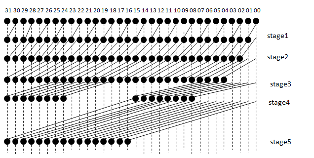 Figure 1: 32 bit Kogge Stone Adder design
The structure of 32-bit KSA design is exposed in Figure 1. This design can be divided into 5 stages [17]. The calculation of Propagate and Generate signals using full adders with carry input that process included in first and second stage. The generation of carry signals which used the values of Propagate and Generate that process included in third and fourth stage. The calculation of sum bits based on the P and carry generation values that is included in the fifth stage [18]. This 32 bit design of KSA is coded by VHDL and viewed the test bench waveform and analyzed the performance and noted the results.
3.2. Brent Kung Adder (BKA)
The BKA calculates the prefixes based on the bit groups. Initially calculate the prefixes values for 2 bit groups. These 2 bit prefix values are used to find the prefix values for the 4 bit groups, that are used to calculate the prefix values for 8 bit groups and so on [19]. Then these prefixes values are used to measure the carry out of the particular bit stage. These carries will be used along with the Group Propagate of the next stage to calculate the Sum bit of that stage [20]. Brent Kung Tree will be using (2log2N-1) stages for any bit design.
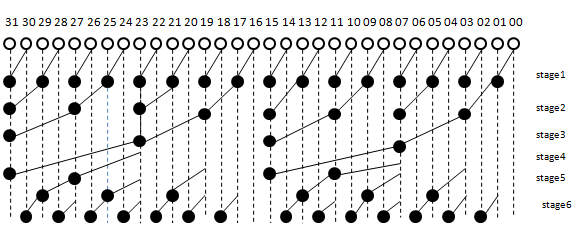 Figure 2: 32 bit Brent Kung Adder design
The structure of 32-bit BKA design is given in Figure 2. Hence the designing of 32- bit adder takes the number of stages will be 9. The fan-out for every bit stage is limited to 2. The above diagram shows the fan out being reduced and the loading on the advance stages being reduced [21]. This 32 bit design of BKA is coded by VHDL and viewed the test bench waveform and analyzed the performance and noted the results.
3.3. Ladner Fischer Adder (LFA)
The LFA tree structures are a family of tree networks between Brent Kung and Sklansky tree. It is very close like to Sklansky PPA, but it calculates the prefix values for odd number bits after that again uses another stage which ripple into the even locations [22]. At higher order bits, to get improved in speeds the cells must still be properly sized or grouped.
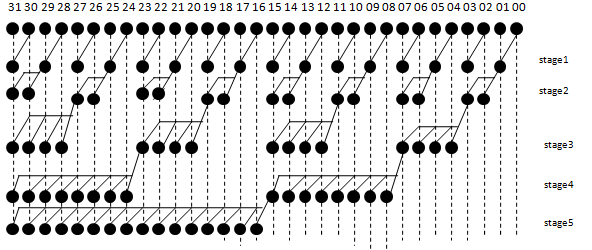 Figure 3: 32 bit Ladner Fischer Adder design
The structure of 32-bit LFA design is exposed in Figure 3. The Ladner Fischer adder is used for high performance arithmetic operation with complicate designs. The LFA consists of black cells and gray cells with 5 stages for 32 bit design. Each black cell encloses only one OR logic gate and two AND logic gates. Each gray cell contains only one AND logic gate [23]. This 32 bit design of LFA is coded by VHDL and viewed the test bench waveform and analysed the performance and noted the results.
4. Simulation results of proposed 32 bit PPA
In this simulation section, took all three types of 32 bit parallel prefix adders (KS, BK, LF) that are discussed above. All the PPA’s are designed on VHDL (Very high speed Hardware Description Language) / Verilog project navigator 14.2i is used for synthesis (Xilinx version) [24]. Simulation results are verified on the basis of area, power and delay. In addition to that the waveforms and the comparison results for all three parallel prefix adders are given.
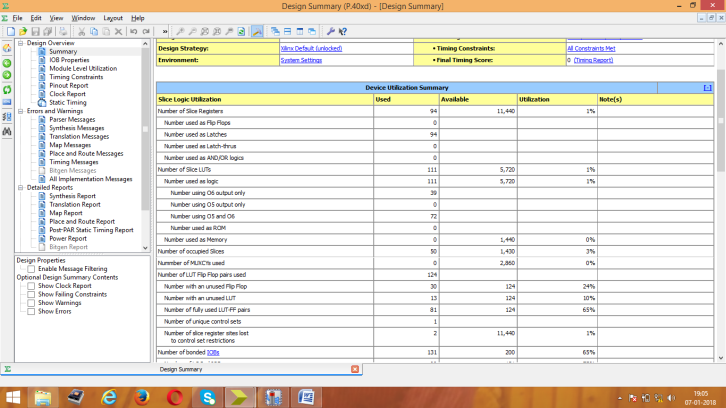 Figure 4: Area Consumption report for KSA
 Figure 5: Power Analyzer report for KSA
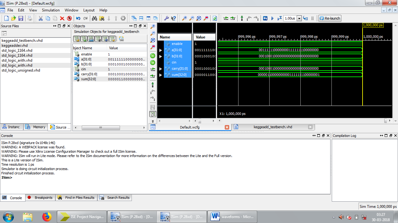 Figure 6: Test bench waveform results of KSA
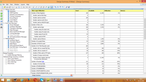 Figure 7: Area Consumption report for BKA
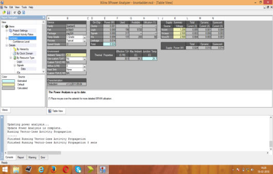 Figure 8: Power Analyzer report for KSA
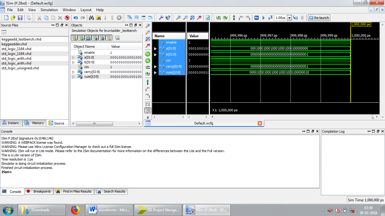 Figure 9: Test bench waveform results of BKA
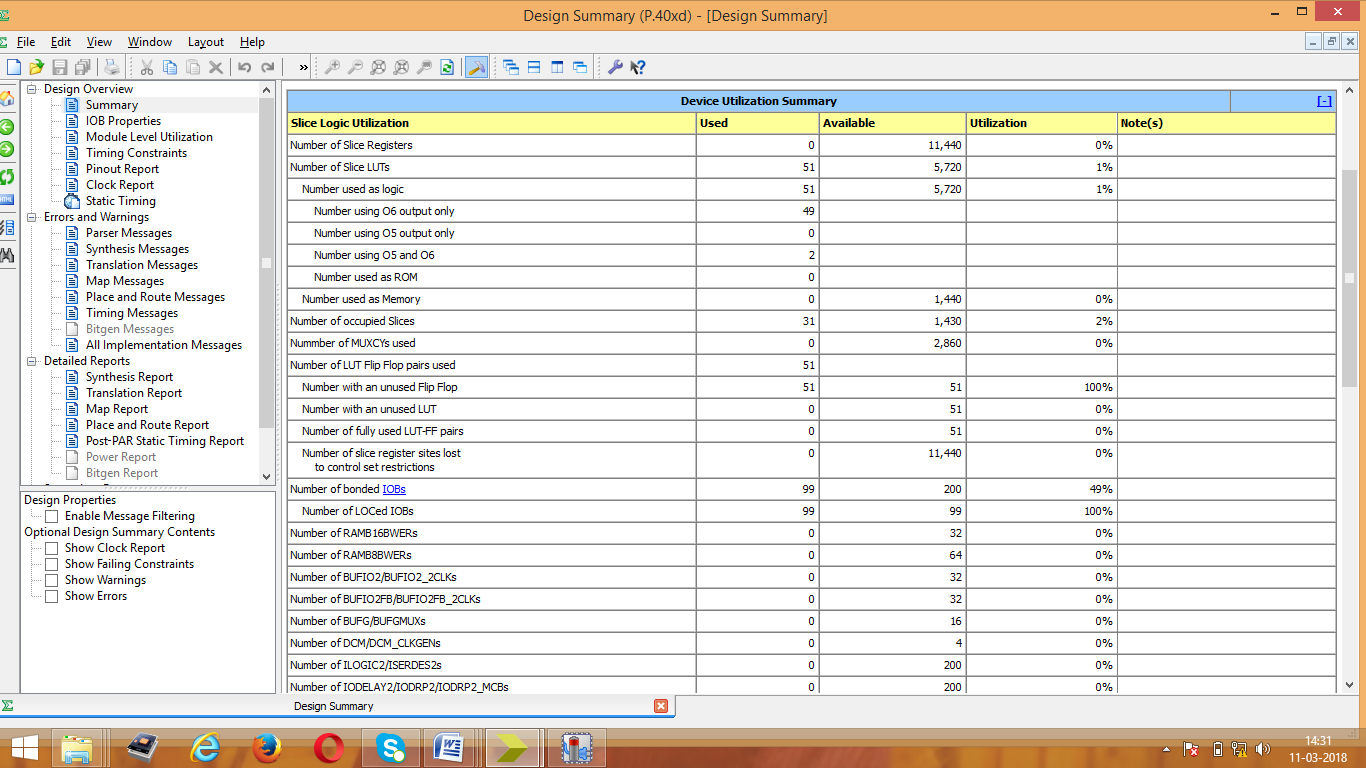 Figure 10: Area Consumption report for LFA
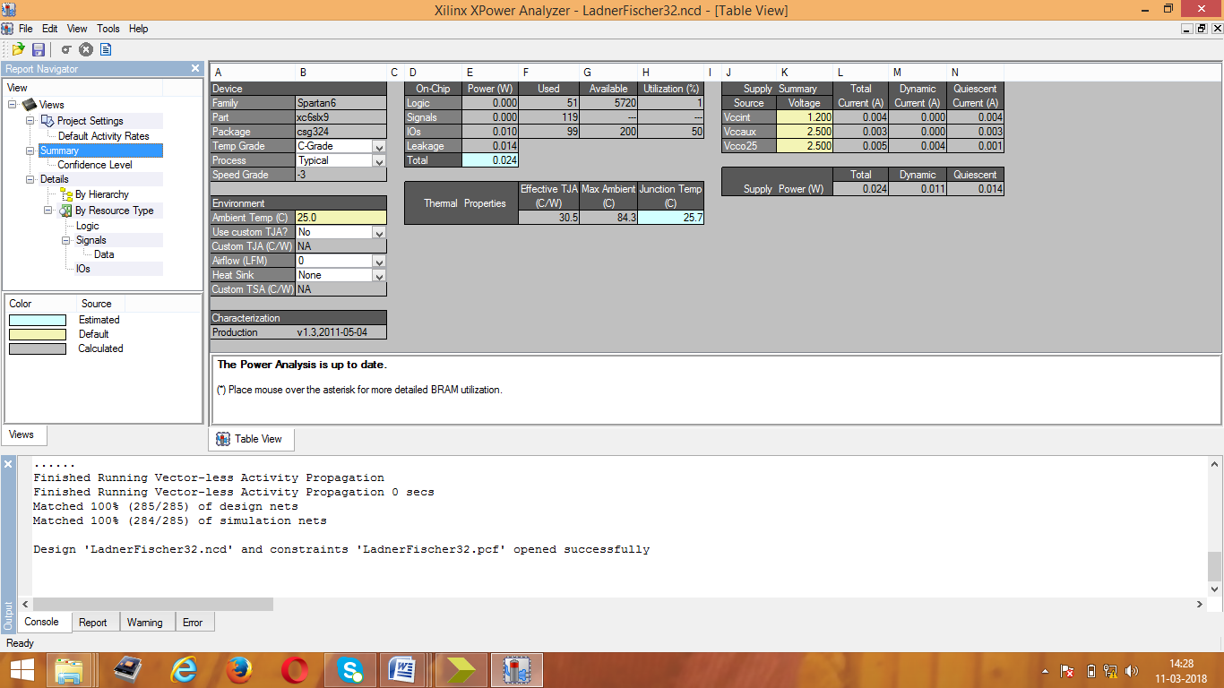 Figure 11: Power Analyzer report for KSA
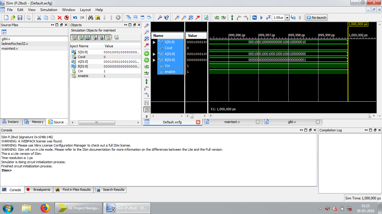 Figure 12: Test bench waveform results of LFA
Area consumption, power analysis, and the test bench waveform of KSA are shown in figures 4, 5, and 6 respectively. Area consumption, power analysis, and the test bench waveform of BKA are shown in figures 7, 8, and 9 respectively. Also the area consumption, power analysis, and the test bench waveform of LFA are shown in figures 10, 11, and 12 respectively.
From the above figures, the comparison results of all three PPA on the aspects of area, delay and power is given in table I. From the analysis, LFA is better due to the less area consumption but the power utilization is more compared to other adders. Normally PPA’s have less delay in any processors while doing addition. Accordance with low power application, KSA is more suitable due to less power utilization in any digital based processors.
Table 1: Comparison results of area, delay and power for various types of PPA
| Adder Types | LUT’s Used | Delay(ns) | Power (mW) |
| Kogge Stone Adder | 189 | 6.483 | 21 |
| Brent kung Adder | 156 | 6.489 | 24 |
| Ladner Fischer Adder | 51 | 21.879 | 24 |
Conclusion
In this paper, an efficient 32 bit Parallel Prefix adders like KSA, BKA, LFA is designed. This proposed 32 bit adder addition operation offers a great advantage in reducing delay. For low power VLSI applications, also the designed adders are compared on the basis of power, area consumption, and delay. The synthesis results reveal that among the proposed adders, KSA is achieved some saving of power-delay product due to less power utilization. But the area delay product is little increased, compared to other adders due to high area consumption. For decreasing the complexity at all performance aspects, further optimization techniques can be achieved on the performance parameters that will be the future work of the paper.
- P. Patronik, S. J. Piestrak, “Design of RNS Reverse Converters with Constant Shifting to Residue Datapath Channels” Journal of Signal Processing Systems, 2017. https://doi.org / 10.1007/s11265-017-1238-6
- D. Kunjan, Shinde, S. Badiger, “Analysis and comparative study of 8-bit adder for embedded application” International Conference on Control, Instrumentation, Communication and Computational Technologies (ICCICCT), 2015. https://doi.org /10.1109/iccicct.2015.7475290
- S. Gedam, Pravin Zode, and Pradnya Zode, “FPGA implementation of hybrid Han-Carlson adder” in 2nd International Conference on Devices Circuits and Systems (ICDCS), 2014. https://doi.org/10.1109/icdcsyst.2014.6926185
- H. Moqadasi, M. B. Ghazvani-Ghoushchi, “A new parallel prefix adder structure with efficient critical delay path and gradded bits efficiency in CMOS 90nm technology” in 23rd Iranian Conference on Electrical Engineering (ICEE), 2015. https://doi.org /10.1109/iraniancee.2015.7146426
- P. Kumar and M. Kiran, “Design of optimal fast adder” in International Conference on Advanced Computing and Communication Systems, 2013. https://doi.org /10.1109/icaccs.2013.6938692
- A. Zarandi, A. Molahosseini, M. Hosseinzadeh, S. Sorouri, S. Antão, and L. Sousa, “Reverse Converter Design via Parallel-Prefix Adders: Novel Components, Methodology, and Implementations” IEEE transactions on very large scale integration (VLSI) systems, 2014. https://doi.org/10.1109/tvlsi.2014.2305392
- Saxena and Pallavi, “Design of low power and high speed Carry Select Adder using Brent Kung adder” in International Conference on VLSI Systems Architecture Technology and Applications (VLSI-SATA), 2015. https://doi.org/10.1109/vlsi-sata.2015.7050465
- N. Shanil Mohamed, T. Y. Siby, “16-bit Velocious Fault Lenient Parallel Prefix Adder” in International Conference on Electronics, Communication and Computational Engineering (ICECCE), 2014. https://doi.org/10.1109/icecce.2014.7086612
- S. A. H. Ejtahed, M. B. Ghaznavi-Ghoushchi, “Design and Implementation of a Power and Area Optimized Reconfigurable Superset Parallel Prefix Adder” in 24th Iranian Conference on Electrical Engineering (ICEE), 2016. https://doi.org/10.1109/iraniancee.2016.7585787
- I. Marouf, M. M. Asad, A. Bakhuraibah and Q. Abu Al-Haija, “Cost Analysis Study of Variable Parallel Prefix Adders Using Altera Cyclone IV FPGA Kit” in International Conference on Electrical and Computing Technologies and Applications (ICECTA), 2017. https://doi.org/10.1109/icecta.2017.8252011
- S. Arthireena, G. Shanmugavadivel, “Efficient Sign Detection using Parallel Prefix Adder” in International Conference on Electrical, Instrumentation and Communication Engineering (ICEICE), 2017. https://doi.org/10.1109/iceice.2017.8191852
- S. Daphni, K. S. Vijula Grace, “A review analysis of parallel prefix adders for better performance in VLSI applications” in Proceedings of 2017 IEEE International Conference on Circuits and Systems (ICCS), 2017. https://doi.org/10.1109/ICCS1.2017.8325971
- F. Liu, Q. Tan, G. Chen, “Formal proof of prefix adders” Mathematical and Computer Modelling, ELSEVIER, 2010. https://doi.org/10.1016/j.mcm.2010.02.008
- S. K. Yezerla, B. Rajendra Naik, “Design and Estimation of delay, power and area for Parallel prefix adders” in Proceedings of RAECS UIET Panjab University Chandigarh., 2014. https://doi.org/10.1109/raecs.2014.6799654
- A. E. Shapiro, F. Atallah, K. Kim, J. Jeong, J. Fischer, E. G. Friedman, “Adaptive power gating of 32-bit Kogge Stone adder” INTEGRATION, the VLSI journal, ELSEVIER, 2015. https://doi.org/10.1016/j.vlsi.2015.12.001
- M. Ozer, M. Eren Çelik, Y. Tukel, A. Bozbey, “Design of RSFQ wave pipelined Kogge–Stone Adder and developing custom compound gates” Cryogenics, ELSEVIER, 2014. https://doi.org/10.1016/j.cryogenics.2014.05.007
- P. Chaitanya kumari, R. Nagendra, “Design of 32 bit Parallel Prefix Adders” IOSR Journal of Electronics and Communication Engineering (IOSR-JECE), 2013. https://doi.org/10.9790/2834-610106
- C. Shilpa, K. D. Shinde, H. V. Nithin, “Design, Implementation and Comparative Analysis of Kogge Stone Adder using CMOS and GDI design: A VLSI Based Approach” in 8th International Conference on Computational Intelligence and Communication Networks, 2016. https://doi.org/10.1109/cicn.2016.117
- N. Poornima, V. S. Kanchana Bhaaskaran, “Area Efficient Hybrid Parallel Prefix Adders” in 2nd International Conference on Nano materials and Technologies (CNT), ELSEVIER, 2014. https://doi.org/10.1016/j.mspro.2015.06.069
- L. Hars, “Applications of Fast Truncated Multiplication in Cryptography” EURASIP Journal on Embedded Systems, 2007. https://doi.org/10.1155/2007/61721
- J. Thomas, R. Pushpangadan, S. Jinesh, “Comparative Study of Performance Vedic Multiplier on The Basis of Adders Used” IEEE International WIE Conference on Electrical and Compter Engineering (WIECON-ECE), 2015. https://doi.org/10.1109/wiecon-ece.2015.7443929
- A. Baliga, “Design of High Speed Adders Using CMOS and Transmission Gates in Submicron Technology: A Comparative Study” in Fourth International Conference on Emerging Trends in Engineering & Technology, Nov 2011. https://doi.org/ 10.1109/icetet.2011.25
- S. Baba Fariddin, E. Vargil Vijay, “Design of Efficient 16-Bit Parallel Prefix Ladner Fischer Adder” International Journal of Computer Applications, 2013. https://doi.org/ 10.5120/13943-1784
- M. Macedo, L. Soares, B. Silveira, C. M. Diniz, Eduardo A. C. da Costa, “Exploring the use of parallel prefix adder topologies into approximate adder circuits” in 24th IEEE International Conference on Electronics, Circuits and Systems (ICECS), 2017. https://doi.org/10.1109/icecs.2017.8292078
Citations by Dimensions
Citations by PlumX
Google Scholar
Scopus
Crossref Citations
- S Daphni, K.S Vijula Grace, "Design an Area Efficient Kogge Stone Adder using Pass Transistor Logic." In 2021 Third International Conference on Intelligent Communication Technologies and Virtual Mobile Networks (ICICV), pp. 614, 2021.
- R. Gowrishankar, N. Sathish Kumar, "Analysis of Efficient 32 Bit Adder Using Tree Grafting Technique." Intelligent Automation & Soft Computing, vol. 35, no. 1, pp. 1197, 2023.
- J. R. Dinesh Kumar, C. Ganesh Babu, "Performance Investigation of a Modified Hybrid Parallel Prefix Adder for Speedy and Lesser Power Computations." IETE Journal of Research, vol. 69, no. 5, pp. 2310, 2023.
- Venkat Subbarao. Manchala, Satyajeet Sahoo, G.Ramana Murthy, "Design and Analysis of 16-bit Spares Kogge Stone adder with proposed 6T-XOR Cell, 1-bit HFA design for High-speed Arithmetic operations." In 2022 International Conference on Communication, Computing and Internet of Things (IC3IoT), pp. 1, 2022.
- Tukur Gupta, Gaurav Verma, Shamim Akhter, "FPGA Implementation and Performance Analysis of Parallel Prefix Structures for Modular Adders Design." Circuits, Systems, and Signal Processing, vol. , no. , pp. , 2024.
- Rishitha Kommineni, Gurram Arunsai, J. V. R. Ravindra, "Low Power, Noise-Immune High Performance Arithmetic Adder Circuit Design Using Modified Parallel Prefix Adders." In Inventive Communication and Computational Technologies, Publisher, Location, 2023.
- A. N. Yakunin, Aung Myo San, Han Myo Htun, "Improving the Operating Efficiency of a Multibit Binary Parallel-Prefix Adder." Russian Microelectronics, vol. 50, no. 7, pp. 491, 2021.
- Gowrishankar R, Sathish Kumar N, Senthilkumar B, "Analysis and Design of Low Area and Highly Energy Efficient Hybrid Adder for Signal Processing Applications." In 2022 Smart Technologies, Communication and Robotics (STCR), pp. 1, 2022.
- Vesapaga Grace Nissi, Satyajeet Sahoo, "Design of Energy-Efficient High-Speed 1-Bit Hybrid Full Adder for Fast Computation." In Digital Communication and Soft Computing Approaches Towards Sustainable Energy Developments, Publisher, Location, 2024.
- Tukur Gupta, Gaurav Verma, Shamim Akhter, "IP-Based Design and Analysis of Parallel Prefix Adder for FPGAs." National Academy Science Letters, vol. , no. , pp. , 2024.
- B N Shashikala, Pooja R, Pavan Prahallad, Ramya S K, M V Ramyashree, "Design and implementation of Kogge-stone, Sparse Kogge-stone and Spanning tree adder." In 2023 International Conference on Smart Systems for applications in Electrical Sciences (ICSSES), pp. 1, 2023.
- D. V. N. Bharathi, Y. Varthamanan, "Implementation of A High Speed Layout Parallel Prefix Adder for Design Applications." In 2024 8th International Conference on Electronics, Communication and Aerospace Technology (ICECA), pp. 194, 2024.
No. of Downloads Per Month
No. of Downloads Per Country
