Performance Investigation of Semiconductor Devices using Commutation-speed based methodology for the application of Boost Power Factor Correction

Adv. Sci. Technol. Eng. Syst. J. 4(1), 258–267 (2019);
 DOI: 10.25046/aj040125
In this paper, behavioral approach has been adopted for the calculation of total power losses that has been further used to derive an analytical model for the conduction and switching losses in a boost Power Factor Correction (PFC) stage of an On-board Charger (OBC). Detailed investigation of power losses can help in finding out ways to improve efficiency and for this purpose, commutation-speed based methodology has been used to split total power losses into their root causes. This gives opportunity to find the impact that an individual part creates on total losses which can serve as a starting point for efficiency improvement. For the analysis, two devices (IGBT with Si diode and IGBT with SiC diode) are used in the considered topology of PFC and a reduction of 40% was calculated when SiC diode was used instead of Si with the same IGBT. Hence it was found that the implemented method proves to be significantly useful in the optimization of efficiency.
1. Introduction
In electric vehicles (xEVs), it is desirable for the on-board charger to operate under maximum efficiency. Therefore, it is of prime importance to accurately calculate the power losses at the system level. A significant part of the power losses arise from the semiconductor devices, being used. A number of different methods are available for the calculation of power losses in semiconductor devices. One of the methods available is physics-based, which requires precise models of the power semiconductor devices and circuits under consideration are simulated numerically with the help of specially designed programs [1]. However in this method, the simulation time tend to be very long which doesn’t seem to be a practical option for system simulations.. Another widely used approach which has been adopted in this paper, is the behavioral modelling of the power losses in which behaviour of the semiconductor device is captured under different operating conditions which is further used to develop simple equations to model the losses. This approach has been proven to give accurate results as discussed in [2,3]. It not only supports simplified calculation but also allows the application of commutation-speed based method in which all devices are switching at the same speed. This methodology makes it possible to split total power losses into their root causes, e.g. capacitive effect, tail current, reverse recovery, forward conduction, reverse conduction [4]. The accurate split-up of power losses give the opportunity to assess and optimize the switching behaviour of power semiconductors at the converter level.
2. Loss Modelling
Power loss modelling involves creation of a generic model that helps in the accurate calculation of total power losses. The main losses associated with a semiconductor device are conduction, switching and gate driving losses but gate driving losses are not discussed in this paper. In general, the loss modelling is done using behavioural model of the device. For the behavioural part, several static and dynamic characterization measurements are conducted that gives insight into the behaviour of the device under different operating conditions. Characterization measurements are performed on the double pulse setup as discussed in [5]. The used setup is shown in Figure 1. For the characterization, one parameter is varied at a time while all other parameters are kept constant at their nominal values. For a higher degree of accuracy, the power loss equations are derived using a model that calculates losses as a function of device current Ic/f, DC link voltage Vdc, junction temperature Tj, gate resistance Rg, area of device Ad/I and gate voltage Vge as elaborated in [2]. The derived equations are used for the calculation of power losses in a boost Power Factor Correction (PFC) stage of an On-board Charger (OBC).
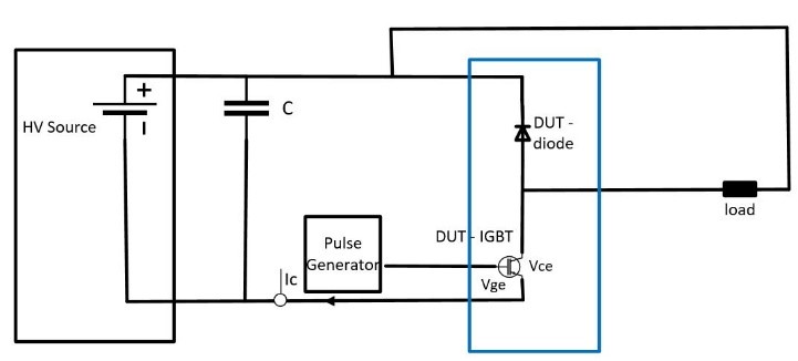 Figure 1 Double pulse setup for device characterization
2.1. Conduction Losses
Conduction losses are determined using instantaneous current and corresponding forward voltage. The simplest and most widely used way to model forward voltage is first order linear approximation consisting of threshold voltage and the drop across series resistance [6]. However, this model is accurate at the nominal operating point whereas the accuracy reduces at all other non-nominal points. A better approach to model forward voltage, which is also used in this work, is to consider the dependency between the considered parameters and voltage as quadratic functions instead of linear. The main advantage of using this approach is its accuracy at non-nominal points as well.
Mathematically, it can be written as [2];
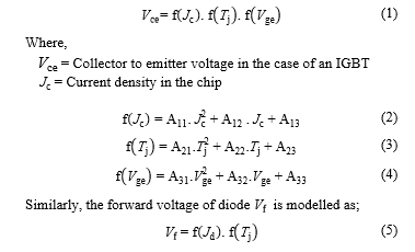 Where,
= Current density of the diode
2.2. Switching Losses
The most accurate way to calculate switching losses is to integrate the area where both voltage and current are overlapping in transition region, but this requires detailed knowledge of transient curves, which isn’t readily available in most cases. A work around of this approach is to use the commutation time in which device is turned on or off and to take the corresponding voltage and currents. This approach is comparatively easier because this information is given in the datasheet [2]. However, these models are fitted at the nominal point and there is increasing error at all other points. That’s why, this paper proposes to use the model presented in [2] where the switching energies as a product of quadratic functions of the considered parameters.
 2.3. Extraction of polynomials for the behavioral model of device
These coefficients ( are determined by fitting a quadratic curve to the characterization measurements. They represent the behaviour of the device and are used to determine the switching and conduction losses at any operating point.
3. Analytical Model for the losses in Boost PFC
Figure 2 shows boost PFC, which is a commonly used PFC topology in an on-board charger. In a boost PFC, there are two sub-sections; rectifier followed by the boost stage that is controlled to ensure unity power factor. Based on the discussion in section 2, an analytical model for the switching and conduction losses of the switching devices in a boost PFC are derived.
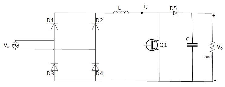 Figure 2 Boost PFC stage of an On-board Charger
The inductor current is sinusoidal; therefore, it can be written as a function of time.
 Where is the peak value of current and is given as;
is the peak value of input voltage and is the output voltage which is equal to the . Whereas the duty cycle for the boost diode is given by;
The average conduction loss in the switch is calculated as given in paper [7]. Integration is performed over half the fundamental cycle and due to symmetrical nature, the integration result is directly multiplied with 2 and then averaged over the fundamental cycle. Mathematically, it is given as;
 Where, T is the fundamental period. On substitution, following expression is obtained.
Similarly, the diode conduction losses are derived as;
4. Splitting of Switching Losses
Experimental measurements give a complete picture of the total losses in the device however it doesn’t explain the contribution of various factors that make up the total losses. To get a deeper insight into the switching losses, the switching events (turn on and turn off) are divided into various regions as explained in [4].
4.1. Turn On
The turning on of the device is divided into two regions as shown in Figure 3; commutation region where the actual current commutation occurs from the diode to the active switch and the reverse recovery region which is influenced by the type of freewheeling diode (FWD), being used.
4.1.1 Region A
The split-up can be achieved by utilizing the device current and voltage waveforms obtained by measurements. Considering device current and voltage shown in Figure 3, the commutation region starts when the gate voltage goes higher than its threshold and the collector current just starts increasing which is marked as to. This region continues till the collector current has reached its steady state value, which is equal to the load current and this time instant is indicated in the Figure as tA. The area from time to to tA is taken as Region A. During the current rise, the collector to emitter voltage drops and this voltage drop is due to the stray inductance of the commutation path, and the rate of change of current as described in [8];
4.1.2 Region B
The second region, reverse recovery part starts when the current through free-wheeling diode (FWD) reaches zero but the diode cannot take the entire voltage yet because of the presence of plasma [9]. Therefore, the current through the active switch continues to increase. The region B constitutes the time when collector current continues to rise due to plasma of FWD till the complete removal of excess carriers and falls subsequently to the steady state value i.e. at time instant tB. The maximum value of collector current depends on the design of diode, gate driver that influences the rate of change of current, the junction temperature and the dc bus voltage [8]. The area from time tA to tB is the Region B.
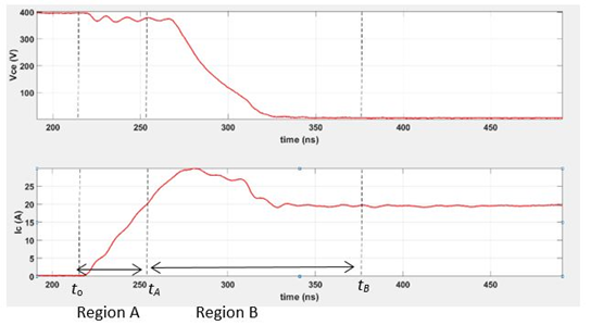 Figure 3 Split-up of the turn on event
4.2. Turn Off
The turn off event shown in Figure 4 is divided into three regions for an IGBT; capacitive region, commutation region and tail current and the speed at which turn off occurs depends on the gate resistance.
4.2.1 Region A
For the IGBT to turn off, it is important that diode takes up the load current which is not possible till voltage across diode has reduced to zero i.e. its junction capacitance needs to be discharged. The current that is used for the discharging of junction capacitance of the diode causes a gradual reduction in active switch’s current i.e. collector current in the case of IGBT. This forms the capacitive region which can be seen in the Figure where current starts falling at time to and the active switch takes up the full voltage at time tA.
4.2.2 Region B
After discharging of junction capacitance, the collector current starts falling rapidly at time tA and that’s when the actual commutation takes place from the active switch to the diode.
4.2.3 Region C
The bipolar devices like IGBT do not turn off till the minority charge carriers have been removed completely. The sweeping of minority carriers from the device takes some time resulting in tail current which starts at tB and continues till current reaches zero, marked in the Figure as tC. The tail current doesn’t exist in the case of MOSFET because it is a unipolar device.
The different regions of turn on, turn off and diode switching losses add up to form total switching losses of the switch. If the contribution of each part on an individual level is known then it can help in the assessment of the impact that they create. This information can be very beneficial in optimizing the efficiency.
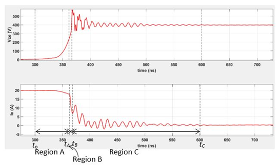 Figure 4 Split-up of the turn off event
5. Compared Devices
To understand the essence of this methodology, it has been implemented on two different discrete devices. One of the devices is Trenshtop-5 IGBT with Rapid Si diode from Infineon [10] and the second device is produced by replacing the Si diode of first device with SiC Schottky diode from Infineon whereas same IGBT is used for both the devices. In this paper, the first device will be referred to as “Full-Si IGBT” and the second device pair as “Hybrid-Si/SiC IGBT”. The nominal values for both the devices are given in Table 1.
Table 1 Nominal values for both the considered devices
| Nominal Values | Ic | Tj | Vdc | Rg |
| Full-Si IGBT | 20 A | 25°C | 400 V | 2.3 Ω |
| Hybrid-Si/SiC IGBT | 20 A | 25°C | 400 V | 14.6 Ω |
6. Effect of Parameters on Split-wise Losses
All the parameters considered here; device current, junction temperature, gate resistance, DC link voltage, area of the device and gate voltage affect the switching losses. To get a better understanding as how each parameter effects the power losses in the devices, these devices are characterized using double pulse setup in which each of these parameter is varied at a time and corresponding total turn on and turn off energies are calculated. The data from characterization measurement is simulated on a specially written program that splits the total turn on and turn off energies into their respective parts as discussed in section 4. The split-up is done for both the considered devices. The results of the simulation are discussed as below where Full-Si IGBT is taken as the reference and the trends where Hybrid-Si/SiC IGBT differs are also explained. The comparison to study the effect of different parameters on switching energies isn’t one to one because the nominal gate resistance is different for the devices.
6.1. Turn On
6.1.1 Effect of Device Current
It is observed that with increasing device currents, the total power losses due to turn on event increase. The trend of turn on energy as a function of device current for Full-Si IGBT and Hybrid-Si/SiC IGBT are shown in Figure 5 and 6 respectively. It can be seen in these figures that the losses due to region A and region B are increasing with increasing current levels. As the value of device current is increased then the rate of change of current decreases i.e. current rises slowly as shown in Figure 7. For a current increase from 5A to 20A, the corresponding rate of change of current is from 0.65 kA/μs to 0.582 kA/μs. This indicates that the losses due to commutation (region A) increase with increasing current. The reason for the increase in losses is due to the direct relation between the value of current and the time taken by the device to reach the nominal value. For higher values of current, device takes more time to rise to that value.
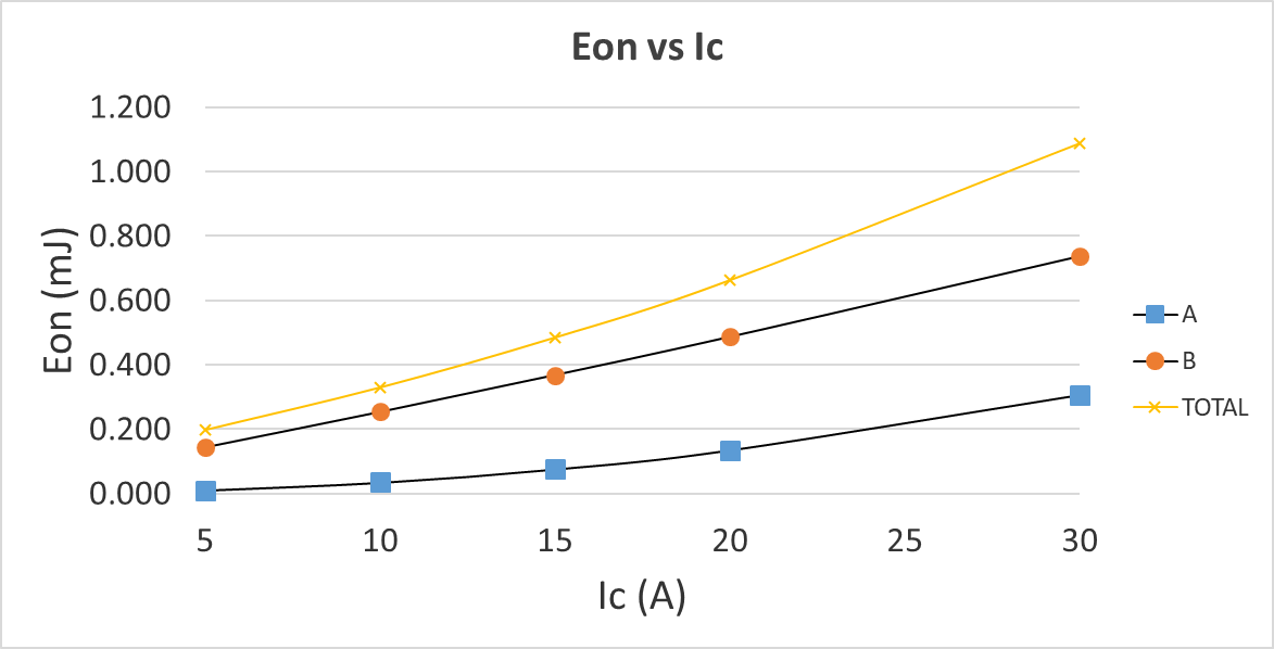 Figure 5 Turn on energy arising from its different root causes as a function of device current (Full-Si IGBT) at Vdc = 400 V, Tj = 25°C and Rg = 14.6 Ω A = commutation, B = reverse recovery
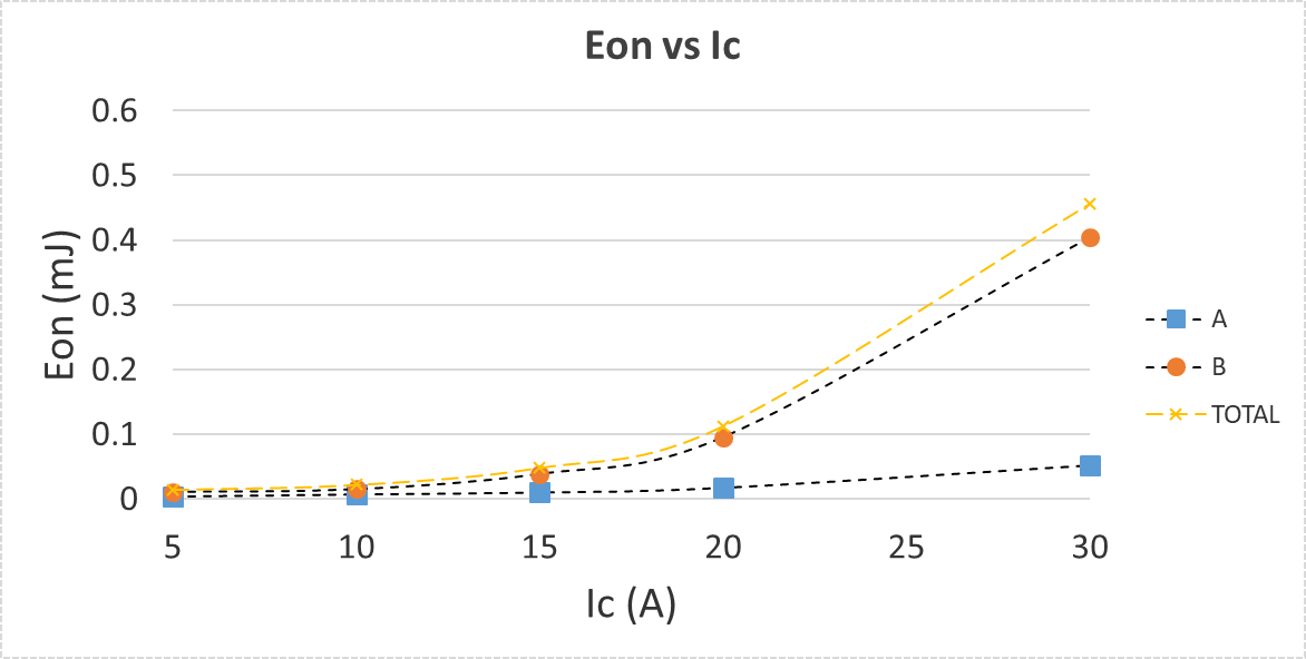 Figure 6 Turn on energy arising from its different root causes as a function of device current (Hybrid-Si/SiC IGBT) at Vdc = 400 V, Tj = 25°C and Rg = 2.3 Ω A = commutation, B = reverse recovery
Losses due to reverse recovery depends on the type of freewheeling diode. In the case of Si diode, which is a bipolar device, the losses due to this region are predominant because Si diode cannot support voltage till the removal of plasma from its PN junction. Therefore, the voltage at IGBT stays higher and allows collector current to rise beyond its nominal point which initiates the sweeping out of plasma from the junction [8]. Therefore, the losses due to reverse recovery (region B) increases with increase in current. Higher current means more number of charge carriers so the time taken by the device to sweep out the excess carriers from PN junction of freewheeling diode is greater as well which leads to increase in losses. On the other hand in the case of unipolar diode like Schottky SiC diode, the losses due to this region are very low because plasma doesn’t exist here and the losses are due to the junction capacitance only.
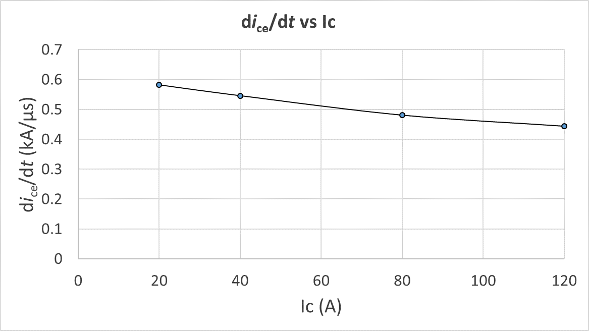 Figure 7 Rate of change of current as function of current (Full-Si IGBT) at Vdc = 400 V, Tj = 25°C and Rg = 14.6 Ω
It is to note here that in turn on losses, major contribution of losses is due to region B which corresponds to reverse recovery for Full-Si IGBT and charging of junction capacitance in the case of Hybrid-Si/SiC IGBT.
6.1.2 Effect of Junction Temperature
With increase in temperature, the threshold voltage at which the IGBT turns on decreases, which leads to faster commutation compared to lower temperatures. However, this has a small effect on the power losses. Increment in temperature leads to a slight decrement in power losses due to region A.
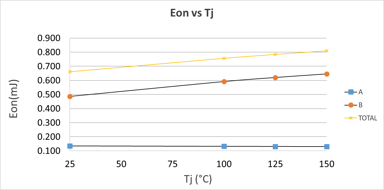 Figure 8 Turn on energy arising from its different root causes as a function of junction temperature (Full-Si IGBT) at Vdc = 400 V, Ic = 20 A and Rg = 14.6 Ω A = commutation, B = reverse recovery
As it can be seen in Figure 8, the losses due to region B increase with increase in temperature. This is because of the fact that the mobility of charge carriers decreases at higher temperature, which slows down the sweeping process of excess carriers from PN junction of diode, leading to increment in losses due to reverse recovery. So, it can be said that at higher temperature, major portion of turn on losses is due to the region B.
Figure 9 shows the dependency of temperature on turn on energy for Hybrid-Si/SiC IGBT. It is seen that the losses due to region A follow the same trend like Full-Si IGBT. This is because the region A is related with the rising current in the IGBT and same IGBT is being used for both the devices. However, the losses due to region B don’t change with temperature. This is because in a SiC diode, the losses in this region do not come from reverse recovery but from the capacitive charge which is independent of the temperature.
 Figure 9 Turn on energy arising from its different root causes as a function of device current (Hybrid-Si/SiC IGBT) at Vdc = 400 V, Ic = 20 A and Rg = 14.6 Ω A = commutation, B = reverse recovery
6.1.3 Effect of DC link Voltage
During region A of turn on, the fall of collector to emitter voltage, is given by (36). The stray inductance is constant and doesn’t change significantly at the nominal current and gate resistance. The only variable is which means that amplitude of increases with the increase in DC link voltage.
In general, the power losses are calculated as integration of the product of and . As is higher for higher values of so the power losses due to region A and B increase. However, the power losses due to region B increase by bigger margin compared to region A as shown in Figure 10. This happens because of the fact that the region B continues till the voltage has reduced to zero, so the time taken by the active switch for its voltage to drop to zero will be longer for higher values of .
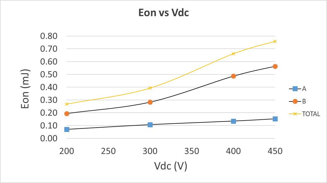 Figure 10 Turn on energy arising from its different root causes as a function of DC link voltage (Full-Si IGBT) at Tj = 25°C, Ic = 20 A and Rg = 14.6 Ω A = commutation, B = reverse recovery
6.1.4 Effect of Gate Resistance
The charging of the gate capacitance determines the switching behavior of the semiconductor device and this is controlled by an external gate resistance. The gate resistance has influence on switching losses; therefore, optimal value of gate resistance should be selected according to the application [11].
A smaller gate resistance leads to shorter rise time which means device switches faster. So, a big gate resistance leads to increment in current rise time i.e. rate of change of current reduces as indicated in Figure 11. This leads to increment in losses due to region A as shown in Figure 12.
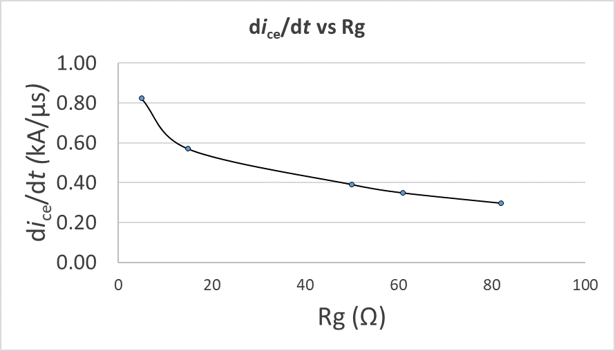 Figure 11 Variation in rate of change of current for different gate resistances at Tj = 25°C, Ic = 20 A and Rg = 14.6 Ω
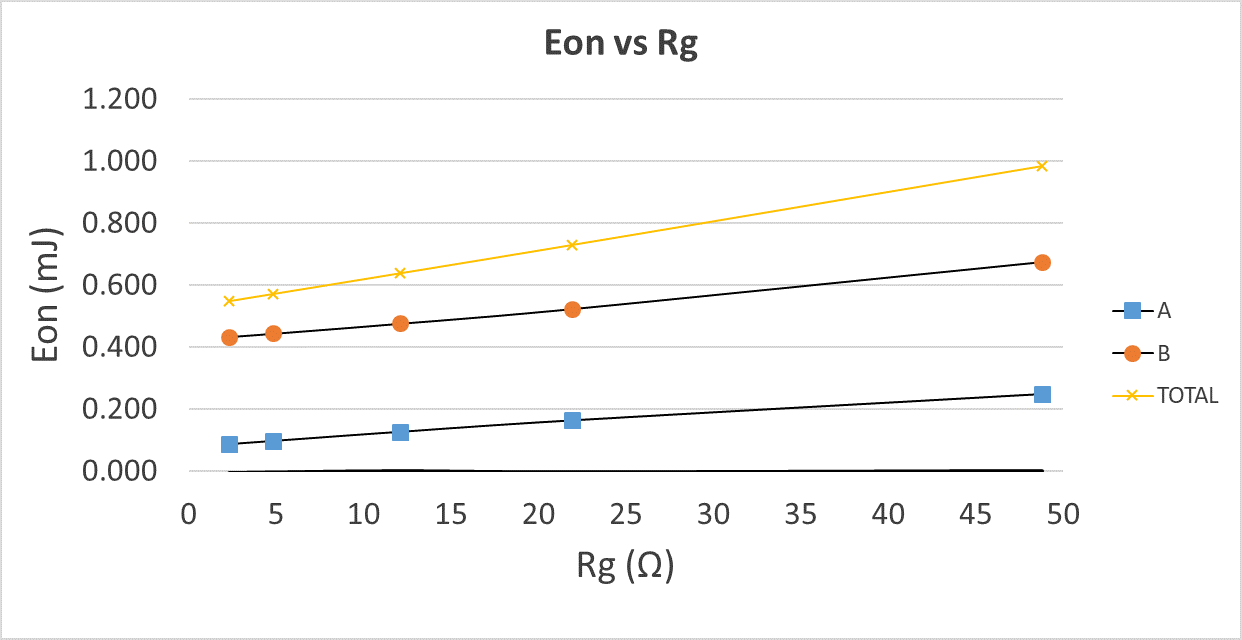 Figure 12 Turn on energy arising from its different root causes as a function of gate resistance (Full-Si IGBT) at Vdc = 400 V, Ic = 20 A and Tj = 25°C A = commutation, B = reverse recovery
With increasing gate resistance, there are two effects as shown in Figure 13; one is that the reverse recovery peak decreases and secondly decreases which indicates that the time taken by the active switch for its voltage to drop to zero is longer compared to a smaller gate resistance. Out of these two effects, the predominant effect is the reduction in which causes increment in the losses due to region B.
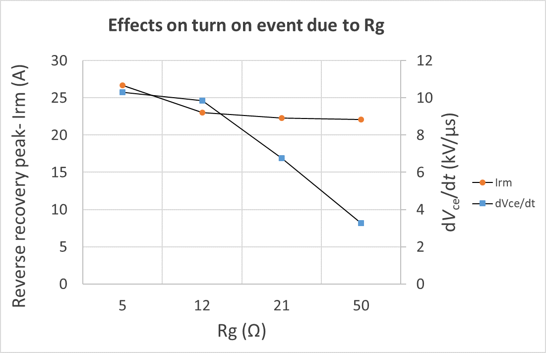 Figure 13 Effects on turn on event due to gate resistance (Full-Si IGBT) at Vdc = 400 V, Ic = 20 A and Tj = 25°C
6.2. Turn Off
6.2.1 Effect of Device Current
With increasing current, the losses due to all regions increase shown in Figure 14. The increment in losses is simply because of the higher value of current. The first region of turn off event, capacitive region, is determined by the rate of change of voltage . If is higher, it means that the junction capacitance of the freewheeling diode discharges at a faster rate and that the diode is able to take the load current faster.
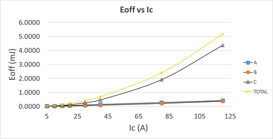 Figure 14 Turn off energy arising from its different root causes as a function of device current (Full-Si IGBT) at Vdc = 400 V, Rg = 14.6 Ω and Tj = 25°C A = capacitive, B = commutation, C = tail current
Here, with increasing current, there is no significant change in the rate of change of voltage as shown in Figure 15; therefore, the losses due to region A increases by small margin. This small increment is due to the beginning of integration from higher value of current.
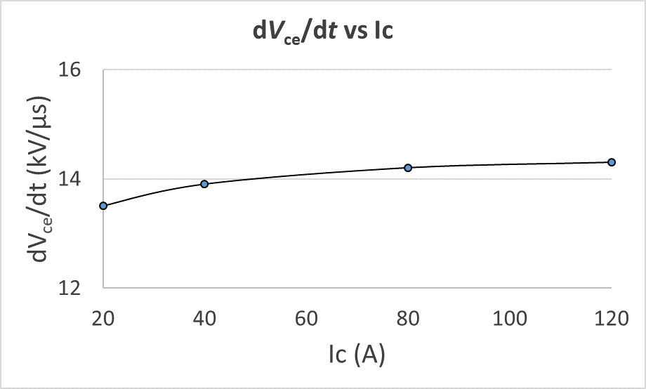 Figure 15 Variation in rate of change of voltage for different current levels (Full-Si IGBT)
It is clear from the Figure 14 that the turn off losses in an IGBT has a big part of losses coming from the tail current.
6.2.2 Effect of Junction Temperature
As temperature increases, the total turn off losses increases as shown in Figure 16. This happens because of the decrement in threshold voltage with increase in temperature so the time taken for the gate voltage to go lower than threshold voltage increases. This leads to slower switching speed; therefore, the power losses due to region B increases with increasing temperature.
The losses due to part C increase with increase in temperature as minority charge carriers take longer to recombine at higher temperatures.
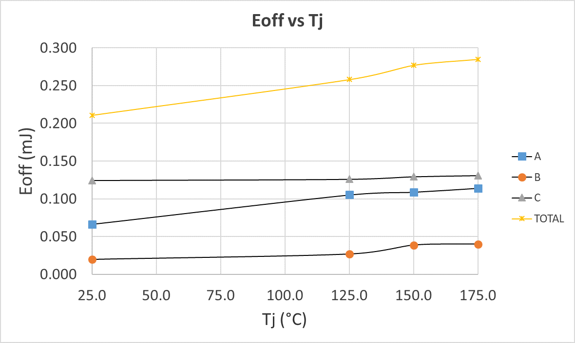 Figure 16 Turn off energy arising from its different root causes as a function junction temperature (Full-Si IGBT) at Vdc = 400 V, Rg = 14.6 Ω and Ic = 20 A A = capacitive, B = commutation, C = tail current
6.2.3 Effect of DC link Voltage
For higher DC link voltage, the turn off losses due to region A, B and C increase. This is because for higher , integration starts from higher value leading to increment in losses.
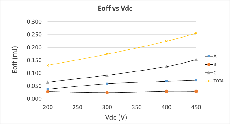 Figure 17 Turn off energy arising from its different root causes as a function DC link voltage (Full-Si IGBT) at Vdc = 400 V, Rg = 14.6 Ω and Ic = 20 A A = capacitive, B = commutation, C = tail current
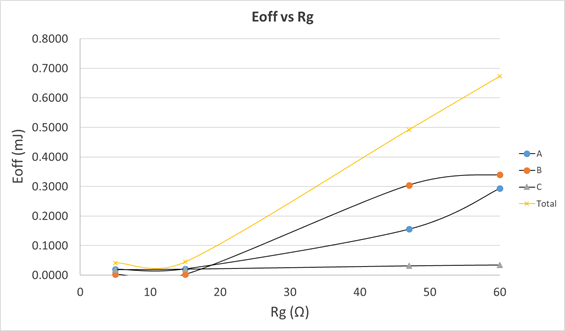 Figure 18 Turn off energy arising from its different root causes as a function gate resistance (Full-Si IGBT) at Vdc = 400 V, Tj = 25°C and Ic = 20 A A = capacitive, B = commutation, C = tail current
6.2.4 Effect of Gate Resistance
If higher value of gate resistance is chosen, then the rate at which device switches reduces. For higher gate resistance, reduces and charging of junction capacitance is slower. This leads to increase in losses due to region A. Because of slower switching speed, the rate at which current falls down decreases leading to increment in losses due to region B. Since the tail current is specific to the IGBT; therefore, the losses due to part C do not change with the change in gate resistance [12].
7. Comparison of Switching Energies for the Considered Devices
Following the discussion of section 6, it is understood that all parameters affect both the devices in certain way. Figure 19 shows the turn on energies as a function of current at the same commutation speed with gate resistance of 5 Ω. At 30A, turn on energy reduces by 38% for Hybrid-Si/SiC IGBT. This is mainly due to the usage of unipolar Schottky SiC diode which doesn’t have reverse recovery, leading to reduction in Eon by such a big margin.
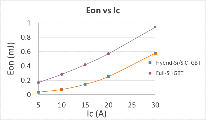 Figure 19 Turn on energy as a function of device current for Full-Si IGBT and Hybrid-Si/SiC IGBT at Rg = 5 Ω, Vdc = 400 V, Tj = 25°C
Figure 20 shows reverse recovery of the diode Erec for different current levels. In the case of Full-Si IGBT, Erec increases with increase in current. However, for Hybrid-Si/SiC IGBT, there is no significant change in Erec, owing to the fact the losses for SiC diode do not originate from reverse recovery but due to the removal of charge carriers from junction capacitance.
8. Application Example
The commutation-speed based method can be applied to any application for the determination of the split-up of power losses at the system level. If the source contributing the most to the total losses is known, then steps can be taken in that direction to improve the efficiency. This method can help in the selection of most suitable device for the specific application. The essence of this method is demonstrated by applying it to previously discussed Boost PFC topology. The specifications of the implemented boost PFC are given in Table 2.
The power losses in this application are due to the rectifier stage, power switches used in boost stage and the losses due to passives. The losses in the power switches are modelled using the behavioral approach as discussed in section 2. Firstly, boost PFC with Full-Si IGBT is simulated in MATLAB where switching based simulation is performed i.e. losses at every switching instant is calculated, summed up and then averaged. This indicates that the simulation follows the same approach for loss calculation as discussed in section 3.
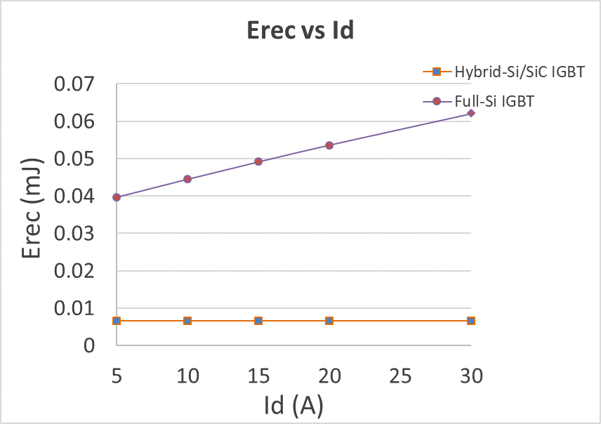 Figure 20 Reverse recovery energy as a function of device current for Full-Si IGBT and Hybrid-Si/SiC IGBT at Rg = 5 Ω, Vdc = 400 V, Tj = 25°C
Table 2 Parameters of the simulated boost PFC topology
| Parameters | Values |
| Vac | 230V |
| Po | 3.3kW |
| Vdc | 400V |
| L | 263.8uH |
| Co | 1300uF |
| fsw | 80kHz |
| Rg | 12Ω |
Figure 21 shows the contribution of different sources of power losses in the boost PFC which are obtained from the simulation. It is seen in the Figure that there are significant losses due to the rectifier and passives in the boost PFC. However, to reduce losses of rectifier, the appropriate option is to use a different topology having less number of diodes in the rectifier stage, which will reduce the conduction losses in the rectifier.
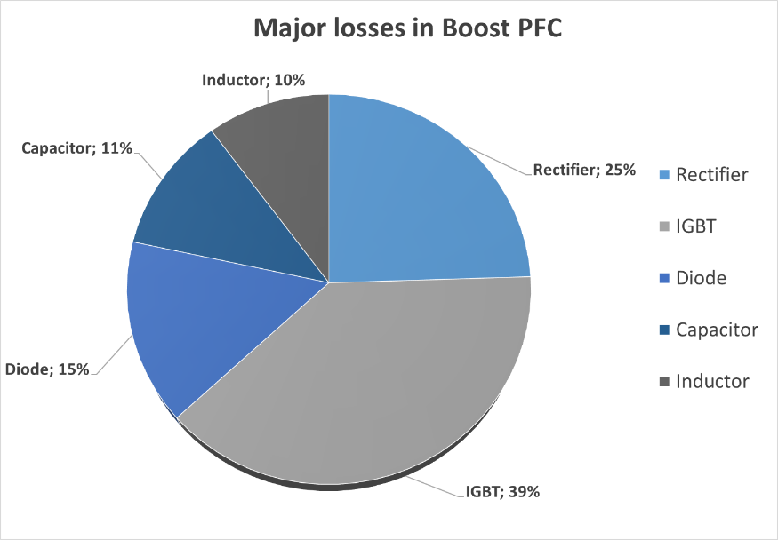 Figure 21 Average power losses in a boost PFC with Full-Si IGBT obtained from simulation at Rg = 12 Ω, Vdc = 400 V, Po = 3.3kW and fsw = 80kHz
The major contribution of losses is coming from the active switch i.e. IGBT. With just this knowledge, it is not easy to determine the efforts that should be taken for the reduction of the power losses. At this point, the commutation-speed based method can be helpful as by splitting the switching losses, one can get a deeper insight into the losses that can help in the identification of the major cause behind the losses. This information can be used to figure out the steps that may be taken to reduce the losses.
This methodology is implemented on the considered two devices, the losses due to rectifier and passives are not considered further and the entire focus is on static and dynamic losses of the semiconductor switches.
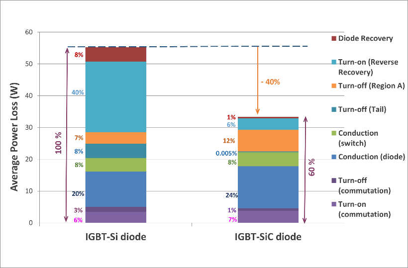 Figure 22 Split-up of the average power losses of the boost PFC for Full-Si IGBT and Hybrid-Si/SiC IGBT at Rg = 12 Ω, Vdc = 400 V
Figure 22 shows the split-up of average power losses for the considered devices according to the regions described in section 4. The contribution of each of these regions help in the assessment of the impact that each region has. Full-Si IGBT is taken as the reference and is marked as 100%. The contribution of all the regions are shown in the Figure as percentages of the total loss of Full-Si IGBT. In Full-Si IGBT, about 40% of power losses are coming from the reverse recovery part of the freewheeling diode (FWD) during turn on event. As discussed earlier, the reverse recovery losses depend on the type of FWD and replacing Full-Si IGBT with Hybrid-Si/SiC IGBT, the losses due to turn on region B decreases by 84% as there is no reverse recovery in a SiC diode and only capacitive losses exist. Besides, a reduction of 89% is observed in the losses due to the diode recovery because there are no excess carriers in a SiC diode. The other major part of losses is due to the tail current, but tail current cannot be eliminated in an IGBT. The only way to eliminate the losses due to tail current is to replace the IGBT with a MOSFET. Another important conclusion that can be drawn from Figure 22 is that conduction losses are slightly greater for SiC diode compared to Si diode. This is because of the forward characteristics of SiC diode.
On the other hand, it is observed that the turn off power losses due to region A are higher for Hybrid-Si/SiC IGBT as compared to Full-Si IGBT. This is mainly because of the junction capacitance of the diode which is bigger for SiC diode so it’s discharging takes longer, leading to higher power losses. This is shown in Figure 23 where under same conditions, Hybrid-Si/SiC IGBT takes 43.2 ns for the discharge of junction capacitance of diode where as Full-Si IGBT takes 36.6 ns.
Figure 24 shows the performance of both the devices for boost PFC at different power levels and it is seen that the efficiency of Hybrid-Si/SiC IGBT is greater than the Full-Si IGBT which is mainly due to the reduction in the losses in diode recovery and reverse recovery part during turn on event. For output power of 3.3kW, efficiency increases by 0.7% for Hybrid-Si/SiC IGBT.
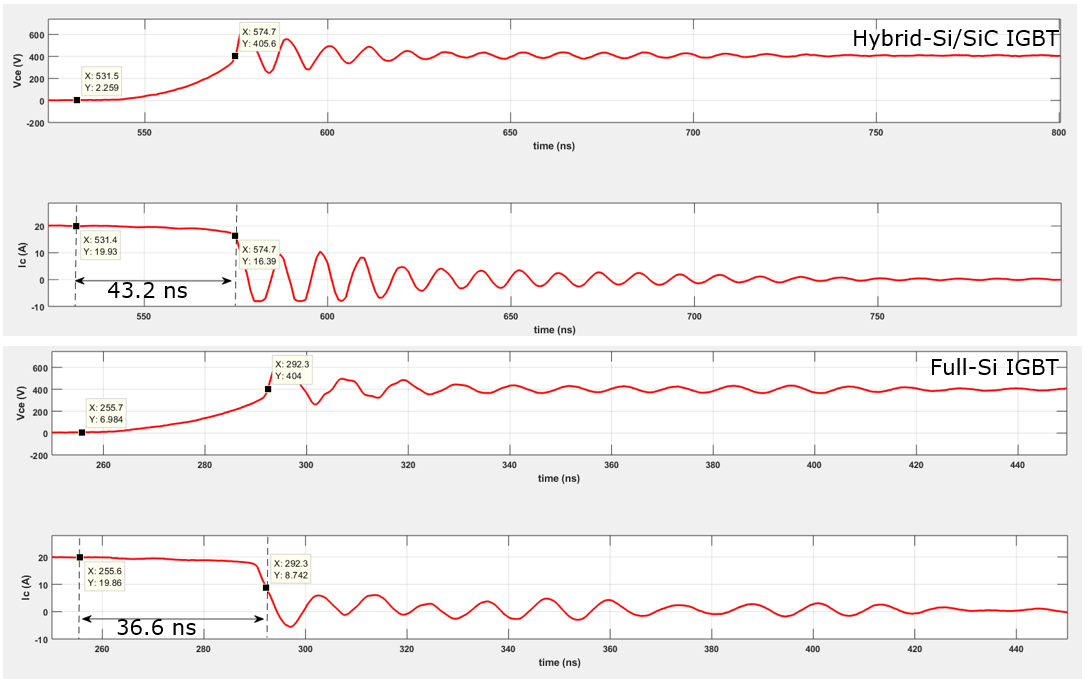 Figure 23 Turn off current for Full-Si IGBT and Hybrid-Si/SiC IGBT
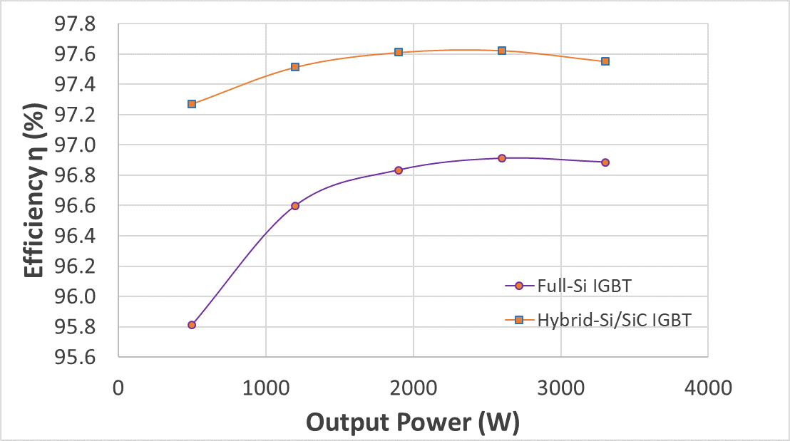 Figure 24 Efficiency comparison of considered devices for different power levels at Vdc = 400 V, Rg = 12 Ω, fsw = 80kHz
9. Conclusion
Traditional power loss calculation gives limited insight into the root cause of the power losses. The commutation-speed based method was applied for the calculation of power losses in the boost PFC of an on-board charger. In this paper, the total switching losses for two discrete devices were split up into their root causes e.g. tail current, reverse recovery. The two combination of devices were IGBT with Si diode and IGBT with SiC diode. The split-up of the considered devices was studied in detail as how the variation in device current Ic/f, DC link voltage Vdc, junction temperature Tj and gate resistance Rg affect the losses. Static and dynamic characterization measurements were performed to model the two devices behaviorally which were then used in boost PFC to calculate the power losses at the system level. It was found that the losses in the switch reduce by 40% just by replacing Si diode with SiC diode for the same IGBT. This reduction in the losses is due to the decrement in the losses in diode recovery and reverse recovery during turn on event indicating that the replacement of just the diode from Si to SiC reduces the power losses by considerable margin. Hence, it can be concluded that this methodology can be applied to any application for the identification of ways to reduce power losses and eventually leading to improvement in efficiency.
Conflict of Interest
The authors declare that there is no conflict of interest
Acknowledgement
We would like to express our gratitude to Rafael Garcia for sharing his knowledge during the course of this research work
- Gebhardt, Fabian, Hauke Vach, and Friedrich W.Fuchs, “Analytical Derivation of Power Semiconductor Losses in MOSFET Multilevel Inverters”, Power Electronics and Motion Control Conference (EPE/PEMC), 2012 15th International. IEEE, 2012.
- Ajay Poonjal Pai Poonjal, Tomas Reiter and Martin Maerz, “A New Behavioral Model for Accurate Loss Calculations in Power Semiconductors”, PCIM Europe 2016; International Exhibition and Conference for Power Electronics, Intelligent Motion, Renewable Energy and Energy Management; Proceedings of. VDE, 2016.
- Ajay Poonjal Pai, “Impact of Silicon Carbide based Power Modules on Mission Profile Efficiency of Automotive Traction Inverters”, PhD Thesis to be published at Friedrich Alexander Universität Erlangen, (Internally available at Infineon).
- Ajay Poonjal Pai, Tomas Reiter and Martin Maerz, “Efficiency Investigation of Full-SiC versus Si-based Automotive Inverter Power Modules at Equal Commutation Speed”, PCIM Europe 2018; International Exhibition and Conference for Power Electronics, Intelligent Motion, Renewable Energy and Energy Management. VDE, 2018.
- Infineon, “HybridPACK Drive, F2660R08A6P2 Power Module with 750V 660A EDT2 Chipset, Hints for Efficient IGBT Switching”, Application Note, 2015, (Internally available at Infineon).
- Kihyun Lee, Kyungsub Jung, Seunghoo Song, Yongsug Suh, Changwoo Kim, Hyoyol Yoo and Sunsoon Park, “Analysis and comparison of high power semiconductor device losses in 5MW PMSG MV wind turbines”, Power Electronics Conference (IPEC-Hiroshima 2014-ECCE-ASIA), 2014 International. IEEE, 2014.
- Ajay Poonjal Pai, Tomas Reiter and Martin Maerz, “An Improved Behavioral Model for Loss Calculations in Automotive Inverter”, EEHE 2016 Wiesloch; Proceedings of 2016.
- Dennis Ward, Iqbal Hussain, Carlos Castro, Andreas Volke, Michael Hornkamp, “Fundamentals of Semiconductors for Hybrid-Electric Powertrain”, Published by Infineon Technologies AG.
- Stefan Linder, “Power Semiconductors”, EPFL Press, 2006.
- Infineon, “TRENCHSTOP™ 5 H5 (High Speed 5) IGBTs”, Datasheet
- Markus Hermwille, “Gate Resistors-Principles and Application”, Semikron International Application Notes.
- Maurice, L. Wuidart, “Drive Circuits for Power MOSFETs and IGBTs”, ST Microelectronics Application Notes.