
A Resolution-Reconfigurable and Power Scalable SAR ADC with Partially Thermometer Coded DAC
Volume 3, Issue 6, Page No 89-96, 2018
Author’s Name: Hao-Min Lina), Chih-Hsuan Lin, Kuei-Ann Wen
View Affiliations
Department of Electronic Engineering, University of National Chiao Tung (NCTU), Hsinchu 300, Taiwan
a)Author to whom correspondence should be addressed. E-mail: ken970054@gmail.com
Adv. Sci. Technol. Eng. Syst. J. 3(6), 89-96 (2018); ![]() DOI: 10.25046/aj030609
DOI: 10.25046/aj030609
Keywords: Reconfigurable, SAR ADC, Thermometer Coded

Export Citations
Power consumption is becoming more and more important in the Internet of Things (IOT). The ADC is the main power hungry in multi-sensor electronic systems and effectively reducing ADC power consumption without affecting ADC characteristics is an important. This paper is extended from the conference paper. The segmented SAR ADC presents reconfigurable 9 to 12-bit DACs with rail-to rail input range, and 3 MSB segmented capacitor arrays are used to improve linearity and lower switching energy than conventional architectures. The dual supply voltage skill separating digital and analog voltage is implemented for achieving low power consumption. In the provided 9 to 12 bits mode, this structure consumes 2.5, 2.8, 3.9 and 9.7 uW and SNDR achieve 52.3, 57.7, 63.2 and 68.6 db respectively, resulting in figure of merit (FoM) 148, 88.8, 66.3 and 88.4 fJ/conversion-step
Received: 15 August 2018, Accepted: 19 October 2018, Published Online: 01 November 2018
1. Introduction
“This paper is an extension of work originally presented in A Low Power Reconfigurable SAR ADC for CMOS MEMS Sensor” [1]. Modern consumer electronics use multi-sensor more and more frequently for CMOS MEM process, the main reason is that has low cost and high integration characteristics of electronic systems. The reported sensors for different capacitive sensitivity have different ranges, such as CMOS MEMS accelerometers are often less than 1 fF/g. To provide greater sensitivity, the readout circuit needs to provide a large capacitance-to-voltage conversion gain. However, large conversion gain amplifies noise and reduces signal-to-noise ratio (SNR). The Correlated double sampling (CDS) and chopper techniques are often used to reduce flicker noise. Moreover, in order to provide a large dynamic range for low to high sensitivity sensors, the programmable gain amplifier (PGA) is implemented. Followed by segmented successive approximation register (SAR) ADC, we choose low power, high resolution, using thermometer code to improve linearity for 3 MSB, and easy-controlling logic circuit to design a reconfigurable ADC that can adjust resolution and power consumption for different requirement. In addition, the power consumption reduction when scaling down the resolution can still maintain the FoM.
On the other hand, the conventional capacitor array architecture performs approximation action and the energy consumption is not efficient. The monotonic capacitor array architecture consumes less than the energy of a conventional capacitor array architecture [2]. The MCS consumes less than monotonic capacitor array architecture [3]. The segment capacity array architecture consumes the same energy as MCS.
In this paper, the proposed SAR ADC can be fabricated under UMC 0.18 mm standard CMOS-MEMS process, which is highly area efficient with MEMS sensor being integrated in single chip. This paper is organized as follows: Section 1 describes ADC ARCHITECTURE including Analysis average energy of Capacitance DAC array structure, analysis of linearity. Section 2 presents ADC ARCHITECTURE DESIGN including system architecture, bootstrap switch and sample-hold, scalable resolution design, control logic and multiplexer Scalable voltage design, comparator, Level shifter. Section 4 describes RESULT and CONCLUSION.
2. ADC Architecture
2.1. Analysis average energy of Capacitance DAC array
In order to achieve greater than 10 bits accuracy, using differential architecture to suppress substrate noise and power noise and have good common mode noise suppression. The conventional SAR ADC architecture is shown in Figure. 1. and often uses of binary weighted capacitor arrays for better linearity. The function block has sample-and-hold, comparator, capacitance DAC array, successive approximation registers. The conventional SAR ADCs are complementary in terms of the fully differential architecture and the following describes the operating procedures on the positive side. In the sampling phase, the bottom plate capacitor on the positive side is charged to the Vip and the top plate capacitor is connected to the common mode voltage Vcm. Next phase, the maximum capacitance bottom plate on the positive side is switched to Vref and the other capacitors on the positive side are switched to GND. At this time, the comparator compares the node voltage Vxp and Vxn. When the node voltage Vxp is greater than Vxn, the most significant bit (MSB) “S11p” is high. Otherwise, “S11p” is low. Then the second maximum capacitor “C2” is switched to VREF and the comparator compares the nodes voltage Vxp and Vxn. The SAR ADC will continue to repeat this process until the least significant (LSB) is determined. Although this trial-and error action is simple, it is not a save power switch procedure.
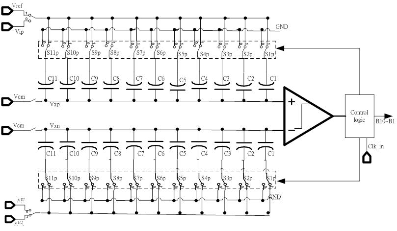 Figure. 1. The conventional SAR ADC architecture
Figure. 2. is a monotonic switching architecture. The monolithic switching method operating procedure is as follows: The input signal via the bootstrapped switch and input signal vip is switched to the capacitance DAC array the top plate on the positive side, which reduces the settling time and increases the input bandwidth. At the same time, the bottom plate capacitor is switched to VREF. Next phase, vip switch to floating and the comparator can directly compare the node voltage of both Vxp and Vxn without switching any capacitor. When the comparator input Vip is greater than Vin, the comparator output “S10p” (MSB) is high. The maximum capacitance bottom plate is switched to GND on the positive side, and the maximum capacitance bottom capacitance remains unchanged on the negative side. The SAR ADC will continue to repeat this process until the LSB is determined. In this procedure, only one capacitor switch is switched to reduce charge conversion for each phase. In addition, the input signal is switched to the maximum capacitance top plate on the capacitance DAC array through the bootstrapped switch, so that the comparator can directly compare the node voltage both Vxp and Vxn. The number of unit capacitors is half of the conventional unit capacitor.
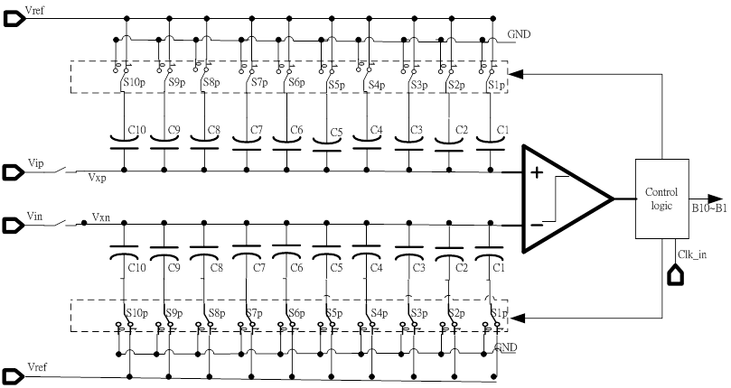 Figure. 2. The monotonic switching architecture [2]
Figure. 3. is a vcm-based switching architecture. The operation procedure of the vcm-based capacitor switching method is as follows: The input signal vip via the bootstrapped switch and is switched to the top capacitance DAC array on the positive side. The bottom plate capacitor is switched to common-mode voltage Vcm. Next phase, vip switch to floating and the comparator can directly compare the node voltage Vxp and Vxn without switching any capacitor. When the comparator input voltage Vxp is greater than Vxn, the “S10p” (MSB) is high. The maximum capacitor bottom plate is switched from Vcm to Vref on the positive side and the maximum capacitance bottom plate is switched from Vcm to GND on the negative side. The SAR ADC will continue to repeat this process until the LSB is determined. Figure 4 is vcm-based switching method flow chart.
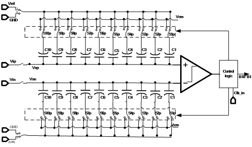 Figure. 3. Vcm-based switching architecture
Moreover, the following is a list of different methods for average switching energy. The average switching energy of conventional switching method, monotonic switching method and vcm-based capacitor switching method are 5459.3 , 1023.8 and 341 respectively.[4, 5]
Table I compares the number of switches, the number of unit capacitors, and switching energy for different methods.
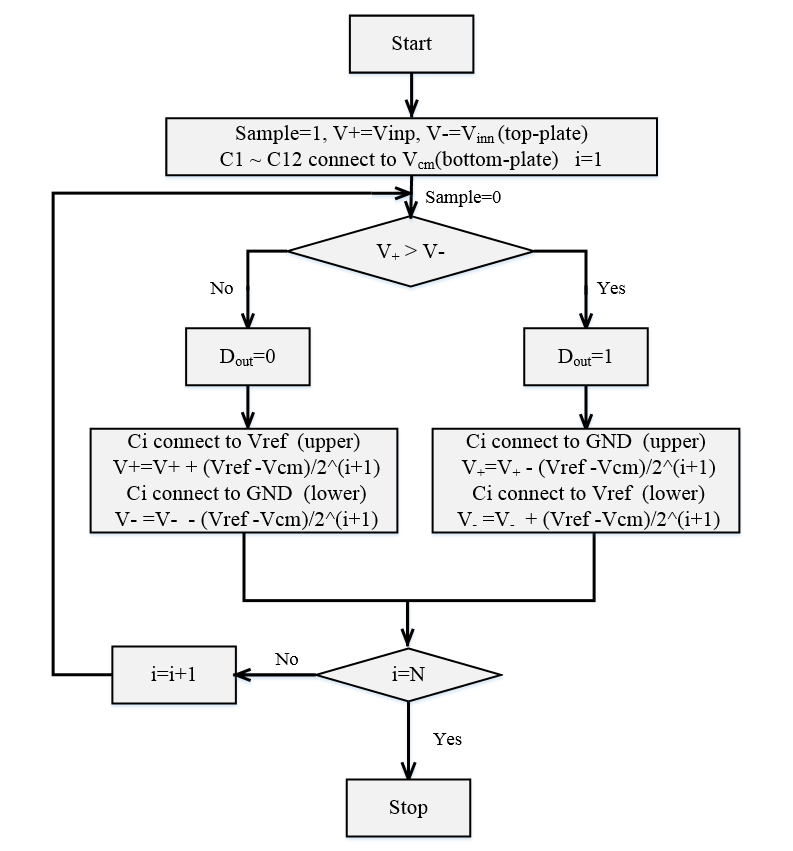 Figure. 4. vcm-based capacitor switching method flow chart
Table 1 Comparison of differentially switch capacitor method
| Parameter | Conventional | Monotonic | Vcm-based |
| No. of Switches | 6n | 4n | 4n |
| No. of Unit Capacitors | 2n | 2n-1 | 2n-1 |
| Switching Energy | “(1)” | “(2)” | “(3)” |
2.2. Analysis of linearity
The conventional binary weighted capacitor array realizes with “radix of 2” and the total number of capacitors is 2n unit capacitors. The proposed partial thermometer coded (or segmented) capacitor array is divided into lower bits and higher bits to implement. The lower bit is implemented with “radix of 2” and the higher bits are implemented with the same capacitor size which is 2N-T-1 unit capacitor. The T is the number of higher bits. The total number of capacitors is same with the capacitor number of capacitors the conventional binary weighted capacitor array, as shown in Figure. 3. The advantage of the proposed partial thermometer coded based DAC is that it can make higher bits (MSB) have better linearity, can reduce DNL, ensure monotonic characteristics, and reduce the glitch phenomenon caused by voltage peak.According to the binary weighted capacitor array, each weighted capacitance can be expressed as [6]
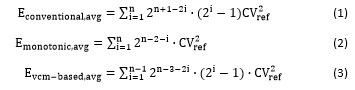 where “i” is an integer representing bit position, is the error term. is unit capacitor.
after the DAC passes n conversion phases, Vxp and Vxn can be expressed as the following expression, “Dn” is the digital output, n is the number of bits, and “Cp” is the parasitic capacitance. ignore the parasitic capacitance and subtract Vxp and Vxn to get the error term, which can be expressed as follow then, subtracting the nominal value which means no error term of from (B-5) expresses as follows
the expected value of Verror is
where “y” is the digital output. Differential nonlinearity (DNL) is the difference of two adjacent code as shown in below: the maximum error is generated from 10….0 to 011…1, variance of the maximum DNL error can be expressed as 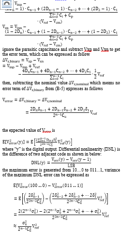
integral nonlinearity (INL) is the difference between the ideal code and the actual code as shown below:
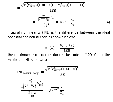
the maximum error occurs during the code in ‘100…0’, so the maximum INL is shown a
segmented DAC’s higher bits MSB, MSB-1, MSB-2 are divided into 7 equal capacitors. The maximum error is generated from 10….0 to 011…1, variance of the maximum DNL error can be expressed as
 where is the mismatch coefficient, “A” is capacitor area and “ ” is the capacitor density parameter. Inserting “(7)” into “(6)” give the capacitor area ratio is . From the results, the DNL in segmented capacitor array is smaller than DNL in binary-weighted array and the size of capacitor array in segmented is smaller than binary-weighted array. In addition, the INL doesn’t change. So, the INL becomes to the main influencing factor and then we can re-calculate the value of unit capacitor through 4.5 1/2 LSB again. At last, a minimum unit capacitor is about 17.83 fF in 12-bit situation.
3. ADC Architecture Design
3.1. System architecture
The segmented SAR ADC system architecture is shown in Figure. 5., divided into sample and hold ,bootstrap switch, dynamic two-stage comparator, synchronous digital control logic including multiplexer and shift register + vcm-based control logic, 3 MSB segmented capacitive DAC including capacitor array and switch, level shifter, resolution Scale control(RS). 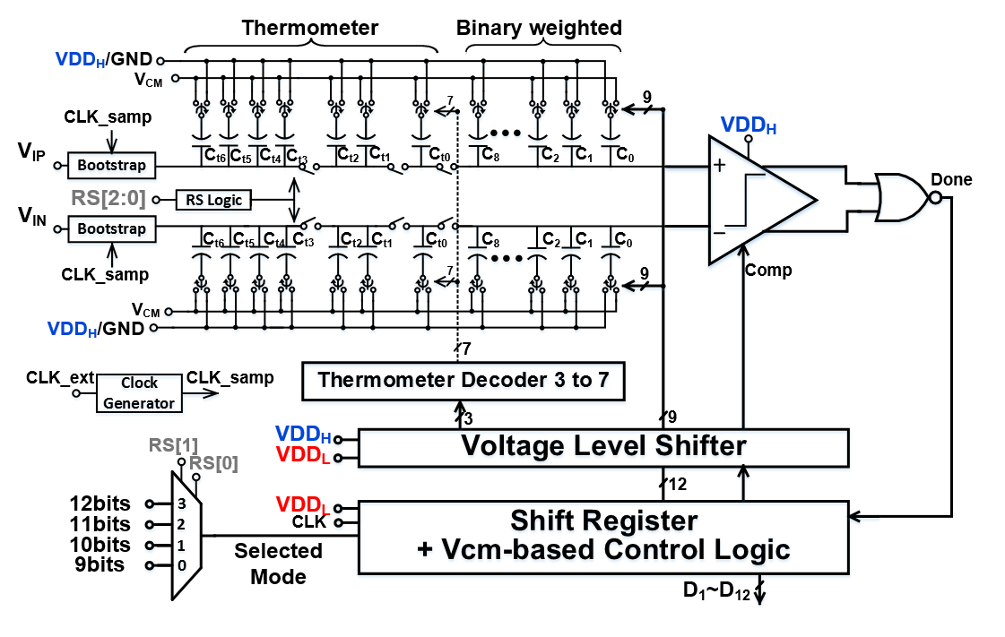 Figure. 5. The segmented SAR ADC system architecture
3.2. Sample and hold
The bootstrap switch with body effect reduction is shown in Figure. 6., which perform sample-and hold function. The input signal is rail-to rail, and must suppress the distortion to at least 12 bits. The operation of the bootstrap switch with body effect reduction is as shown in Figure. 7. [7]. When clk=high, input signal is Vin and the node VG voltage is fixed at the voltage AVDD+Vin. So that the on-resistance of MOS(“SW”) on-resistance keep a small constant value, which can improve the linearity. In addition, “M15” is turned on to make the bulk node of MOS (“SW”) is connected to Vin, which can cancel the body effect. Therefore, this can reduce the significant distortion. When clk=low, the bulk of MOS (“SW”) will be connected to GND to avoid back-gate driven. According to simulation and the sample rate 50 Ks/s and and Nyquist input frequency in 8192 sample point, taking FFT(fast Fourier transform) for bootstrap switch and output capacitor and get SNDR is greater than 87.2 db, ENOB(effective number of bits) is greater than 14.29 bits. The relation of SNDR to ENOB equation can be derived, SNDR=6.02*ENOB+1.76.
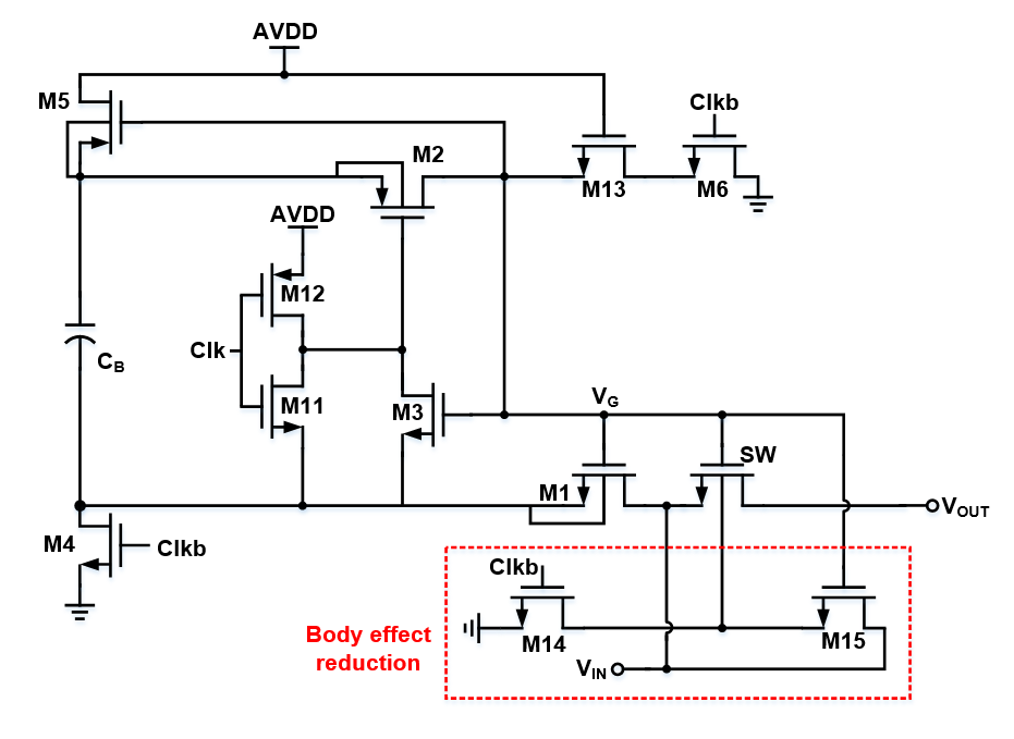 Figure. 6. The bootstrap switch with body effect reduction
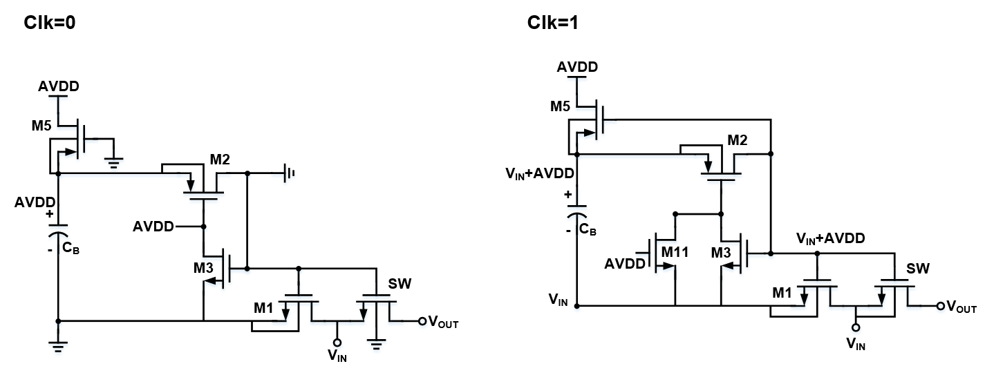 Figure. 7. The operation of the bootstrap switch with body effect reduction
3.3. Scalable resolution design
The proposed segmented capacitor array is shown Figure. 8. The 3 MSB capacitor bottom plate is divided into seven equal capacitances and the T is 3. Moreover, the seven equal capacitances can be controlled by three-to-seven bit binary-to-thermometer decoder logic. The remaining switches can be controlled by binary weighted mode. Insert the switch on the MSB capacitor top plate to decouple from the other capacitor array, using these insertion switches to divide into different resolutions and the corresponding FOM is obtained. Moreover, the resolution signal (RS1, RS2) is used to control insertion switch on the 3 MSB capacitor top plate and the control method is two-to-three bit binary-to-thermometer decoder. The three-to-seven binary-to-thermometer logic expression is as follows.
T6 = D1 D2 D3 T5 = D1 D2 T4 = D1 (D2 + D3)
T3 = D1 T2 = D1 + (D2 D3) T1 = D1 + D2 T0 = D1 + D2 + D3
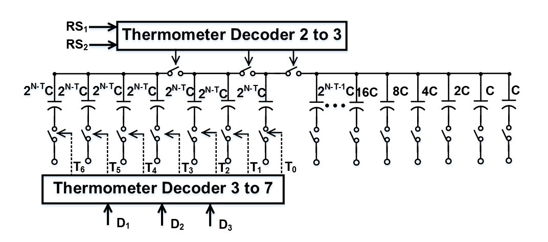 Figure. 8. The proposed segmented capacitor array
3.4. Control logic and multiplexer
The synchronous clock control is adopted in the proposed SAR ADC and is shown Figure. 9. The external clock (CLK_COMP) triggers the comparator and input in the clock divider to generate sampling rate (CLK_SAMP) of system. In addition, extra NOR gate is used to detect the result of comparator. When CLK_COMP is low in the reset mode, the output Vop and Von are both low and the Done signal is high. When CLK_COMP is high in the comparison mode, the output Vop and Von are either high or low and the Done signal goes low that means the comparison is finished.
The shift signal S[1:13] shows the current conversion cycle and will trigger the corresponding digital control logic and capacitor switching signal as shown in Figure. 10. The multiplexers control the necessary shift signal to pass through shift register and stop each conversion with resolution scale (RS[1], RS[0]) signal. For 9 to 12 bit mode, after the corresponding shift signal S[10] to S[13] goes to high, the STOP signal will be triggered and reset all the block of SAR ADC for avoiding the waste of power consumption.
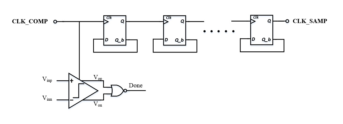 Figure. 9. Synchronous clock generator
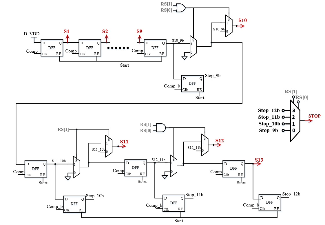 Figure. 10. Shift register with multiplexer
The synchronous clock waveform of digital circuit is shown Figure. 11. The clock waveform shows that START goes to high when sampling end. Then the first COMP_CLK goes to high and so does S[1], which means SAR ADC is in first conversion cycle. The second period of COMP_CLK is also the same way to enter to the next conversion. In the end, the last COMP_CLK goes to low and STOP will rise to high to finish the number bit-mode of conversion.
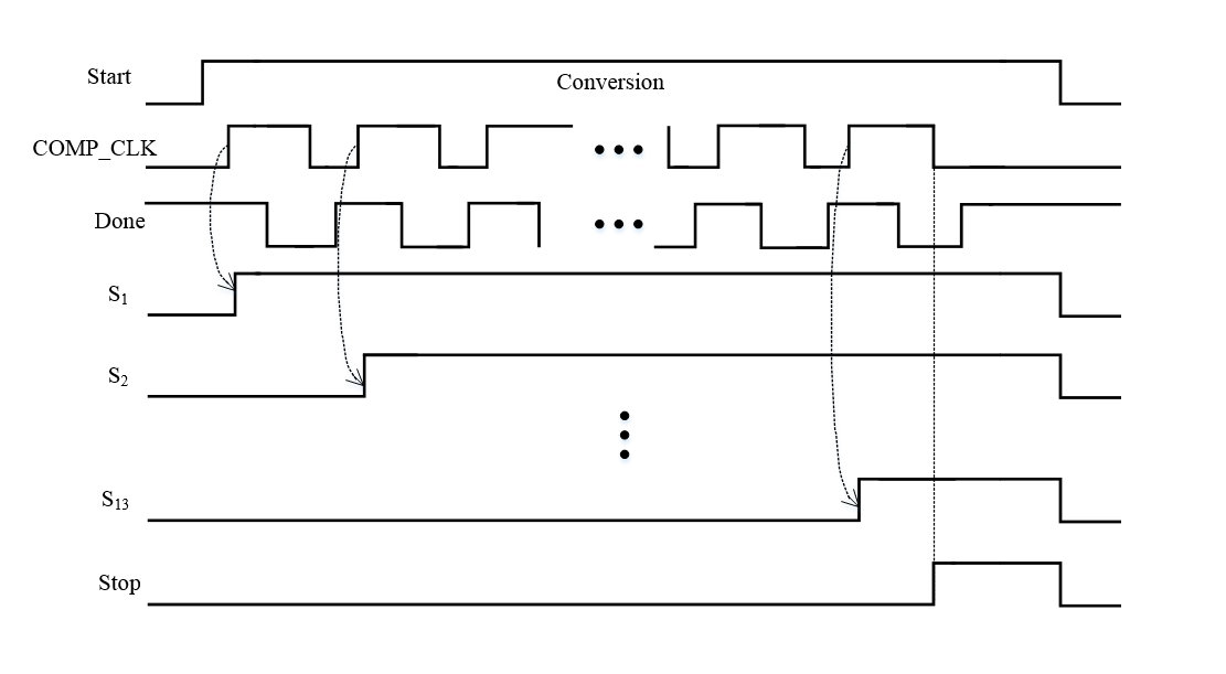 Figure. 11. Synchronous clock waveform of digital circuit
The control logic circuit of Vcm-based switching is shown Figure. 12. For the first comparison cycle, we use XOR gate with S[1] and S[2] to generate X1 that is the range of first comparison cycle. Before the first result of comparator is decided, the MSB capacitor is still connected to Vcm. Therefore, reuse the X1, COMP_CLK and Done input to the AND gate to generate the CLK_Vcm1. After the first result of comparator is decided, MSB capacitor is connected to Vref or GND depending on the output of comparator in the rest of the comparison cycle. Here we utilize the XOR gate with X12 and CLK_Vcm1 to generate CLK_Vref1. X12 is the signal created by S[1] and S[13] with XOR gate, and it represents the range of first to last comparison cycle. From the second comparison cycle to the last comparison cycle, the same methods are used to generates CLK_VCM2 to CLK_VCM12 expect for addition of the OR gate with the previous Xi comparison cycle to keep the capacitor in Vcm voltage. CLK_Vref2 ~ CLK_Vref12 also utilize the XOR gate with X12 and the current CLK_Vcmi to generate.
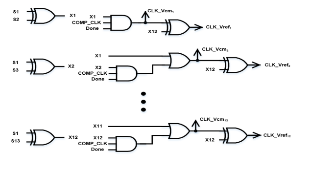 Figure. 11. Control logic circuit of Vcm-based switching
Schematic and timing diagram of the DAC control logic based on [2] is shown in Figure. 12. At the rising edge of COMP_CLK, a D-flip-flop samples the output of the comparator at the current conversion. If the output is high, the relevant capacitor is switched from Vcm to GND. If the output is low, the relevant capacitor is switched from Vcm to Vref. After the decision signal of control voltage is confirmed, the level shifter should be used to switch the digital voltage domain to analog voltage domain that makes correct charge distribution. The output buffer stores the digital output code decided by comparator and reveals when the STOP signal triggers in the end of the bit-conversion.
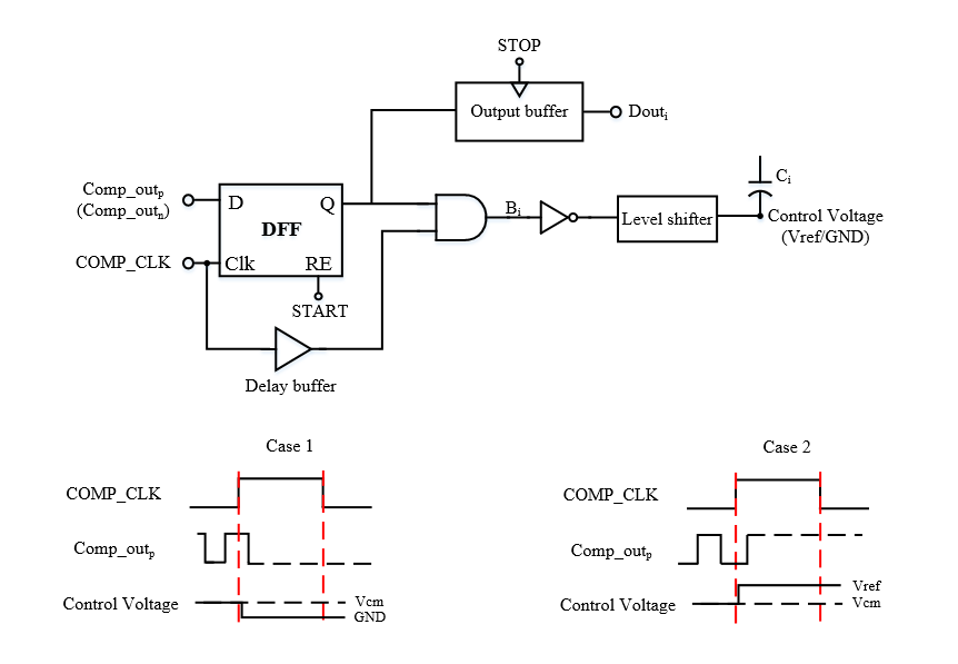 Figure. 12. DAC control logic
3.5. Scalable voltage design
The system architecture energy analysis can be simplified into analog block, comparator, digital block, level shift. The system architecture of the SAR ADC with the Dual supply voltage is shown
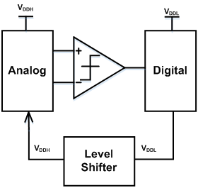 Figure. 13. Since the level shift is the bridge between analog and a digital and can be divided into analog block and digital block.
The energy-per-conversion is given by ![]()
where “CL(n)” is the effective capacitance being charged and discharged, and is relative to the resolution .
In [8], the energy of a dynamic regenerative comparator is derived. When applied to a n-bit SAR ADC that requires n comparisons per conversion, the comparator energy-per-conversion can be derived as [9]
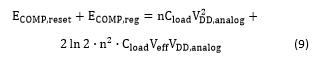
 where “Cload” is the capacitive load of comparator, “Veff” is the transistor overdrive voltage, and “VDD” is the power supply of comparator. The energy is also proportional to the analog supply voltage.
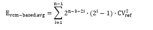
The Vcm-based average switching energy of DAC we use in this ADC design is shown in formula “(3)”.
The energy is proportional to and capacitor size. Capacitor size depends on the limitation of capacitor mismatch and Vref is corresponding to the power supply voltage of comparator. According to formula “(3)”, “(8)”, “(9)”, scaling down VDD is an effective method to reduce energy. Figure. 13. The system architecture of the SAR ADC with the Dual supply voltage
3.6. Comparator
The comparator consists of two stage is shown in Figure. 14. The first stage Preamp has a fixed current source (“M5”) and the current source operates in saturation. Consequently, the drain current is only slightly changed and the dynamic offset is only slightly changed. The pre-amp’s voltage gain is about 5~10 and helpful to reduce the second-level input referred noise. In addition, the input pair operates in weak inversion to achieve lower input referred noise. The second stage consists of a simple voltage amplifier and a positive feedback amplifier that makes the output reach rail-to-rail. The operation of dynamic comparator has two phases. In reset phase, the CLK is low voltage and the node TI_N, TI_P has been pre-charged to VDD by device “M3”, “M4”. The output VOP, VON of comparator has been discharged to ground by device “M13”, “M14”. When it comes to comparison phase, the CLK goes to high voltage. CLK enables “M5” which producing a current path and starts to discharge the capacitors on node TI_N, TI_P through “M1”, “M2”. “M11” and “M12” are used as a switch to sense the voltage difference between input signal VIP and VIN.
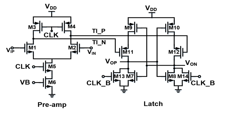 Figure. 14. Dynamic two-stage comparator with a current source
In comparison phase, the input-referred noise can be estimated by [10]:
![]() where “k” is Boltzmann constant, “T” is the Kelvin temperature which is set to 300 K,transconductance “gm1,2” and integration time “Tint” is shown below:
where “k” is Boltzmann constant, “T” is the Kelvin temperature which is set to 300 K,transconductance “gm1,2” and integration time “Tint” is shown below:
![]()
![]() where “Vthermal”, the thermal voltage, is equal to 25 mV, “Vthreshold” is threshold voltage of input pair equals to 460 mV, CTI_P and CTI_N is the parasitic capacitance of node. TI_P and TI_N. Inserting “(11)” and “(12)” into “(9)” gives
where “Vthermal”, the thermal voltage, is equal to 25 mV, “Vthreshold” is threshold voltage of input pair equals to 460 mV, CTI_P and CTI_N is the parasitic capacitance of node. TI_P and TI_N. Inserting “(11)” and “(12)” into “(9)” gives
![]() At 12-bit mode with 1.8 analog supply voltage, 1/2 LSB is equal 0.44 mV. It means that should be designed smaller than 0.44 mV. According to (13), re-derived CTI_P, CTI_N as follow: substituting all the value that mentioned before, CTI_P, CTI_N can be designed over 11 fF to let the thermal noise of comparator in the same order as quantization noise of the ADC.For Vcm-based switching method, the input common voltage of comparator maintains at Vcm voltage that the offset belongs to static offset and it doesn’t affect the accuracy but it will decrease input range, thus degrading the signal-to-noise ratio [11]. From Monte-carol simulation, the comparator offset for 1.8 V, 1.2 V, 1.0 V is 7.83 mV, 8.28 mV and 7.86 mV respectively. The formula of SNR can be derived as follow: where is the input voltage range influenced by offset and “VLSB is the least significant bit (LSB) voltage. Compare without offset simulation and the SNR of with offset simulation decrease by 0.04, 0.06 and 0.07 dB respectively. Therefore, the effect of ENOB is little influence.
At 12-bit mode with 1.8 analog supply voltage, 1/2 LSB is equal 0.44 mV. It means that should be designed smaller than 0.44 mV. According to (13), re-derived CTI_P, CTI_N as follow: substituting all the value that mentioned before, CTI_P, CTI_N can be designed over 11 fF to let the thermal noise of comparator in the same order as quantization noise of the ADC.For Vcm-based switching method, the input common voltage of comparator maintains at Vcm voltage that the offset belongs to static offset and it doesn’t affect the accuracy but it will decrease input range, thus degrading the signal-to-noise ratio [11]. From Monte-carol simulation, the comparator offset for 1.8 V, 1.2 V, 1.0 V is 7.83 mV, 8.28 mV and 7.86 mV respectively. The formula of SNR can be derived as follow: where is the input voltage range influenced by offset and “VLSB is the least significant bit (LSB) voltage. Compare without offset simulation and the SNR of with offset simulation decrease by 0.04, 0.06 and 0.07 dB respectively. Therefore, the effect of ENOB is little influence.
3.7. Level shifter
The conventional level shifter has large delay and power consumption. The CMLS (contention mitigated level shift) has less delay and power consumption, the reason is that “MN1”, “MP3”, “MN2”, “MP4” form quasi-inverter, the node OUT voltages are pulled faster than conventional level shifter. The schematic of level shifter is shown in Figure. 15. The two PMOS act as a swing-restoring load. Assuming the input signal, IN, is low, “MN1” is turned on and provides a conducting path to ground while “MN2” is cut off. Therefore, OUT is pulled down to ground. The operation reverses when the input signal, IN, is switched to high
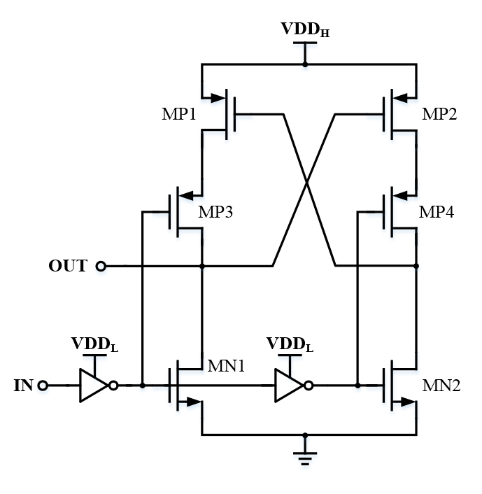 Figure. 15. Schematic of level shifter [12]
Table 2 shows comparison of the SAR ADC simulation result
| This work | [4] | [13] | ||||
| Resolution | 12 bit | 11 bit | 10 bit | 9 bit | 10 bit | 12 bit |
| Technology(um) | 0.18 | 0.13 | 0.18 | |||
|
Supply voltage(V) (Analog/Digital) |
1.8/ 0.9 |
1.2/0.9 | 1.0/0.4 |
1.8/ 1.8 |
||
| Area(mm2) | 0.35 | 0.19 | 2.38 | |||
| Sampling Rate(KS/s) | 50 | 1 | 200 | |||
| SNDR(dB) | 68.6 | 63.2 | 57.7 | 52.3 | 56.54 | 69.6 |
| Power(uW) | 9.7 | 3.9 | 2.8 | 2.5 | 0.05 | 41.5 |
| FoMa(fJ/conversion) | 88.4 | 66.3 | 88.8 | 148 | 94.5 | 84.6 |
4. Result and Discussion
This paper presents a reconfigurable SAR ADC for multi-sensor application. The transistor level simulation is operated by Cadence Spectre for 1P6M 0.18 um CMOS technology. The maximum sampling rate is 50 KS/s, and input frequency is at Nyquist rate and gets 256 number of points for the FFT analysis. Analog supply voltage is at 1.8 V (12 bit), 1.2 V (11, 10, 9 bit). Digital supply voltage is at 0.9 V and the clock duty cycle is 50%. The reconfigurable SAR ADC has achieved 4 mode including 12/11/10/9 bits and corresponding performance SNDR are 68.6/63.2/57.7/52.3 dB at input frequency (fin) 6.25/25/25/25 KS/s respectively. Table II shows comparison of the SAR ADC result.For the accuracy of capacitor array, the placement of the DAC are arranged by common-centroid layout to enhance matching and the dummy capacitors are added around capacitor array to keep from etching effect around edge. The layout of capacitor array separate into two parts, one is for 10 to 12 bit that T0 to T6 means the corresponding capacitor controlled by thermometer decoder and the other is for the 1 to 9 bit. The overall core area is 810 x 430 um2. Layout of capacitor array is shown Figure. 16. And the segmented SAR ADC layout plan including capacitor array, switch array, comparator, sample-and-hold(S/H), SAR logic is shown Figure. 17.
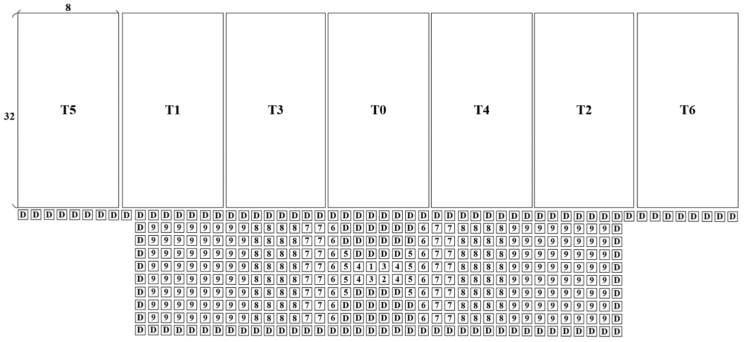 Figure. 16. Layout of capacitor array
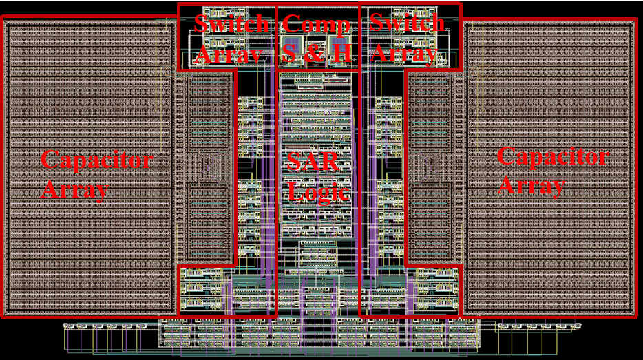 Figure. 17. The segmented SAR ADC layout plan
Acknowledgment
This research was sponsored in part by the National Science Council of Taiwan under grant of MOST 106-2911-I-009-301.The authors appreciate the UMC and the National Chip Implementation Center (CIC), Taiwan, for supporting the CMOS chip manufacturing.
- H.-M. Lin and K.-A. Wen, “A low power reconfigurable SAR ADC for CMOS MEMS sensor,” in SoC Design Conference (ISOCC), 2017 International, 2017, pp. 7-8.
- C. C. Liu, S. J. Chang, G. Y. Huang, and Y. Z. Lin, “A 10-bit 50-MS/s SAR ADC With a Monotonic Capacitor Switching Procedure,” IEEE Journal of Solid-State Circuits, vol. 45, no. 4, pp. 731-740, 2010.
- V. Hariprasath, J. Guerber, S. H. Lee, and U. K. Moon, “Merged capacitor switching based SAR ADC with highest switching energy-efficiency,” Electronics Letters, vol. 46, no. 9, pp. 620-621, 2010.
- S. Haenzsche and R. Schüffny, “Analysis of a charge redistribution SAR ADC with partially thermometer coded DAC,” in 2013 European Conference on Circuit Theory and Design (ECCTD), 2013, pp. 1-4.
- Yuan-Fu Lyu , ” A Low Power 10-Bit 500-KS/s Delta-Modulated Successive Approximation Register Analog-to-Digital Converter for Implantable Medical Devices ,” Master , Institute of Electronics , National Chiao Tung University , Hsin chu , 2012.
- Liao, Bo-Shi, ” Power-Efficient Successive-Approximation Register Analog-to-Digital Converter, “Master , Institute of Electronics Engineering, National Taiwan University, 2016.
- S. Wang and C. Dehollain, “Design of a rail-to-rail 460 kS/s 10-bit SAR ADC for capacitive sensor interface,” in 2013 IEEE 20th International Conference on Electronics, Circuits, and Systems (ICECS), 2013, pp. 453-456.
- Z. Dai, C. Svensson, and A. Alvandpour, “Power consumption bounds for SAR ADCs,” in 2011 20th European Conference on Circuit Theory and Design (ECCTD), 2011, pp. 556-559.
- M. Yip and A. P. Chandrakasan, “A Resolution-Reconfigurable 5-to-10-Bit 0.4-to-1 V Power Scalable SAR ADC for Sensor Applications,” IEEE Journal of Solid-State Circuits, vol. 48, no. 6, pp. 1453-1464, 2013.
- M. v. Elzakker, E. v. Tuijl, P. Geraedts, D. Schinkel, E. A. M. Klumperink, and B. Nauta, “A 10-bit Charge-Redistribution ADC Consuming 1.9 mW at 1 MS/s,” IEEE Journal of Solid-State Circuits, vol. 45, no. 5, pp. 1007-1015, 2010.
- D. Zhang, A. Bhide, and A. Alvandpour, “A 53-nW 9.1-ENOB 1-kS/s SAR ADC in 0.13-mm CMOS for Medical Implant Devices,” IEEE Journal of Solid-State Circuits, vol. 47, no. 7, pp. 1585-1593, 2012.
- C. Q. Tran, H. Kawaguchi, and T. Sakurai, “Low-power high-speed level shifter design for block-level dynamic voltage scaling environment,” in 2005 International Conference on Integrated Circuit Design and Technology, 2005. ICICDT 2005., 2005, pp. 229-232.
- Z. Yan, U. F. Chio, W. He-Gong, S. Sai-Weng, U. Seng-Pan, and R. P. Martins, “Linearity analysis on a series-split capacitor array for high-speed SAR ADCs,” in 2008 51st Midwest Symposium on Circuits and Systems, 2008, pp. 922-925.